IMPLEMENTATION OF HIGH SPEED SECURE
COMMUNICATION BETWEEN MULTIPLE FPGA SYSTEMS
USING RTOS
1Reasearch Scholar, Aurora's Research &Technological Institute, Warangal, India. 2Associate Professor, Aurora's Research &Technological Institute, Warangal,India.
3Application Engineer at Unistring Tech Solutions Pvt Ltd, Hyderabad, India.
Abstract - Reconfigurable system like FPGA platform has the potential to provide the performance benefits of ASICs and the flexibility of processors. FPGA based embedded system have become a platform for the implementation of cryptographic algorithms. In this paper we are going to implement cryptographic algorithm utilizing threads run by an RTOS [Real time operating systems] on FPGA systems. Since RTOS is an efficient tool to optimize the software runtime as the code complexity grows, by distributing the tasks into multiple threads. As an RTOS we have chosen Xilkernel and TEA [Tiny Encryption Algorithm] for implementing Cryptographic algorithms. Our project mainly focus on the major issue that two threads running separately on each board can communicate with each other via RS232 communication link. The system that is used for establishing the serial communication between the multiple FPGA systems is UART (universal Asynchronous Receiver Transmitter).The proposed architecture is synthesized using Xilinx ISE 13.2 and it will be implemented on XC3S500e Spartan 3E FPGA board for hardware implementation and testing. The necessary software for this design is written using the feature-rich c/c++ code editor and compilation environment provided within the SDK.
Keywords – Cryptography, FPGA, RTOS, SDK, TEA,
Threads, XPS.
I. INTRODUCTION
Reconfigurable System like FPGA platform has the potential to provide the performance benefits of ASICs and the flexibility of processors. An FPGA is a collection of programmable gates embedded in a flexible interconnect network that can contain hard or soft microprocessors. FPGAs combine the programmability of processors with the performance of custom hardware. As FPGAs can provide a useful balance between performance and flexibility, they become the primary source of computation in many critical embedded systems.
FPGA based embedded system have become a platform for the implementation of cryptographic algorithms, which needs large number of bit-level operations, and that can be done efficiently on FPGA. The merit of our paper lies in the implementation of cryptographic algorithm utilizing threads, run by an
RTOS on FPGA systems, which is quite challenging in this reconfigurable architecture domain. The usage of RTOS is advantageous in many respects, as RTOS is an efficient tool to optimize the software runtime as the code complexity grows, by distributing the tasks into multiple threads. Better and safer synchronization and resource management are also major advantages of an RTOS. [1].
The Micro Blaze has a versatile interconnect system to support a variety of embedded applications. Micro Blaze’s primary I/O bus, the Core Connect PLB bus, is a traditional system-memory mapped transaction bus with master/slave capability. Many aspects of the Micro Blaze can be user configured: cache size, pipeline depth (3-stage or 5-stage), embedded peripherals, memory management unit, and bus-interfaces can be customized. The area-optimized version of Micro Blaze, which uses a 3-stage pipeline, sacrifices clock-frequency for reduced logic-area. The performance-optimized version expands the execution-pipeline to 5-stages. Also, key processor instructions which are rarely used but more expensive to implement in hardware can be selectively added/removed (i.e. multiply, divide, and floating-point ops.) This customization enables a developer to make the appropriate design tradeoffs for a specific set of host hardware and application software requirements.
With the memory management unit, Micro Blaze is capable of hosting operating systems requiring hardware-based paging and protection, such as the Linux kernel. Otherwise it is limited to operating systems with a simplified protection and virtual memory-model: e.g. Free RTOS or Linux without MMU support. Micro Blaze’s overall throughput is substantially less than a comparable hardened CPU-core. Xilinx's EDK (Embedded Development Kit) is the development package for building Micro Blaze (and PowerPC) embedded processor systems in Xilinx FPGAs. Hosted in the Eclipse IDE, the project manager consists of two separate environments: XPS and SDK. [2].
Designers use XPS (Xilinx Platform Studio) to configure and build the hardware specification of their embedded system (processor core, memory-controller, I/O peripherals, etc.) The XPS converts the designer's platform specification into a synthesizable RTL description (VHDL), and writes a set of scripts to automate the implementation of the embedded system (from RTL to the bit stream-file.) For the Micro Blaze core, the EDK normally generates an encrypted (non human-readable) net list, but the processor description
(written in VHDL) can be purchased from Xilinx. The SDK handles the software that will execute on the embedded system. Powered by the GNU tool chain (GNU Compiler Collection, GNU Debugger), the SDK enables programmers to write, compile, and debug C/C++ applications for their embedded system.
FPGA demonstrates good performance and logic capacity by exploiting parallelism. At present single FPGA platform can play multi-functions, including control, filter and system. FPGA design flow is a three-step process consisting of design entry, implementation, and verification stages, as shown in Fig 1.The full design flow is an iterative process of entering, implementing, and verifying the design until it is correct and complete. [3].
II. HARDWARE AND SOFTWARE REQUIREMENTS
A. SPARTAN-3E FPGA FAMILY
The five-member family offers densities ranging from 100,000 to 1.6 million system gates. These Spartan-3E enhancements, combined with advanced 90 nm process technology, deliver more functionality and bandwidth per dollar than was previously possible, setting new standards in the programmable logic industry. Because of their exceptionally low cost, Spartan-3E FPGAs are ideally suited to a wide range of consumer electronics applications, including broadband access, home networking, display/projection, and digital television equipment. The Spartan-3E family is a superior alternative to mask programmed ASICs. FPGAs avoid the high initial cost, the lengthy development cycles, and the inherent inflexibility of conventional ASICs.
Figure.1: Spartan 3E FPGA
B. MICROBLAZE
In terms of its instruction-set architecture, Micro Blaze is very similar to the RISC-based DLX architecture described in a popular computer architecture book by Patterson and Hennessy. With few exceptions, the Micro Blaze can issue
a new instruction every cycle, maintaining single-cycle throughput under most circumstances.
The Micro Blaze has a versatile interconnect system to support a variety of embedded applications. Micro Blaze's primary I/O bus, the Core Connect PLB bus, is a traditional system-memory mapped transaction bus with master/slave capability. A newer version of the Micro Blaze, supported in both Spartan-6 and Virtex-6 implementations, as well as the 7-Series, supports the AXI specification. The majority of vendor-supplied and third-party IP interface to PLB directly (or through PLB to OPB bus bridge.) For access to local-memory (FPGA BRAM), Micro Blaze uses a dedicated LMB bus, which reduces loading on the other buses. User-defined coprocessors are supported through a dedicated FIFO-style connection called FSL (Fast Simplex Link). The coprocessor(s) interface can accelerate computationally intensive algorithms by offloading parts or the entirety of the computation to a user-designed hardware module.
C. EMBEDDED DEVELOPMENT KIT [EDK]
The Xilinx Embedded Development Kit (EDK) is a suite of tools and Intellectual Property (IP) that enables you to design a complete embedded processor system for implementation In a Xilinx Field Programmable Gate Array (FPGA) device. Xilinx's EDK is the development package for building Micro Blaze (and PowerPC) embedded processor systems in Xilinx FPGAs.
Xilinx Platform Studio (XPS) is the development environment used for designing the hardware portion of your embedded processor system. From the XPS software, you can design a complete embedded processor system for implementation within a Xilinx FPGA device. Designers use XPS (Xilinx Platform Studio) to configure and build the hardware specification of their embedded system (processor core, memory-controller, I/O peripherals, etc.) The XPS converts the designer's platform specification into a synthesizable RTL description (VHDL), and writes a set of scripts to automate the implementation of the embedded system (from RTL to the bit stream-file.) For the Micro Blaze core, the EDK normally generates an encrypted (non human-readable) net list, but the processor description (written in VHDL) can be purchased from Xilinx.
D. SOFTWARE DEVELOPMENT KIT (SDK)
The Xilinx software development kit (SDK) is an integrated development environment, complementary to XPS, that is used for C/C++ embedded software application creation and verification. You use SDK to develop the software that is used on the embedded platform built in XPS. SDK is based on the Eclipse open source tool suite. When you open SDK, you create a workspace. A workspace is a directory location that is used by SDK to store project data and metadata. You must provide an initial workspace location when SDK is
launched. You can create multiple workspaces to more easily manage multiple software versions. A software project contains one or more source files, along with the necessary header files, to allow compilation and generation of a binary output (Executable and Linkable Format) file. A workspace can contain multiple software projects. Each software project must have a corresponding board support package. You must have a hardware platform for your design. The hardware platform is the embedded hardware design that is created in XPS. The hardware platform includes the XML-based hardware description file, the bit stream file, and the BMM file. When you import the XML file into SDK, you import the hardware platform. Multiple hardware platforms can exist in a single workspace.
The SDK handles the software that will execute on the embedded system. Powered by the GNU tool chain (GNU Compiler Collection, GNU Debugger), the SDK enables programmers to write, compile, and debug C/C++ applications for their embedded system. Xilinx includes a cycle-accurate instruction set simulator (ISS), giving programmers the choice of testing their software in simulation, or using a suitable FPGA-board to download and execute on the actual system.
Figure.2: Basic Embedded Design process flow
E. XILKERNEL
Xilkernel is a small, robust, and modular kernel. It is highly integrated with the Platform Studio framework and is a free software library that you get with the Xilinx Embedded Development Kit (EDK). It allows a very high degree of customization, letting users tailor the kernel to an optimal level both in terms of size and functionality. It supports the core features required in a lightweight embedded kernel, with a POSIX API. Xilkernel works on both the Micro Blaze™ and PowerPC™ 405 processors. Xilkernel IPC services can be used to implement higher level services such as networking, video, and audio. Fig 3 shows the different Xilkernal modules for user applications. [4].
Figure.3: Xilkernal modules
F. THREAD MANAGEMENT
Xilkernel supports the basic POSIX threads API. Thread creation and manipulation is done in the exact same way as defined in POSIX. Threads are identified by a unique thread identifier. The thread identifier is of type pthread. This thread identifier is used to uniquely identify a thread for an operation. Threads created in the system have a kernel wrapper to which they return control to when they terminate. Therefore a specific exit function is not required at the end of the thread’s code. Thread stack is allocated automatically on behalf of the thread from a pool of Block Starting Symbol (BSS) memory that is statically allocated depending on the maximum number of threads in the system. You can also assign a custom piece of memory as the stack for each thread that they create dynamically. The entire thread module is optional and can be configured in or out as a part of the software specification.[5]-[7].
III. IMPLEMENTATION
The main theme of the paper is to implement Real time Communication between two FPGA’s for cryptographic applications. Data from FPGA 1 is not directly transmitted to the FPGA-2 rather than that we are applying cryptographic mechanism. According to cryptography, the input data is being transmitted from the transmitter to receiver by converting the text into a specific format which cannot be read by the unauthorized (third person) person. This text is called as cipher text. The process of transforming the plain text into cipher text is called as encryption. This cipher text is transmitted to the receiver end where the cipher text is again retransformed back to plain text. This process is called as Decryption. As we are performing encryption at transmitter section and decryption at receiver section, implementing a secure communication between two FPGA’s. In this paper we are implementing this cryptography between two configurable devices (FPGA’s) for effective real time communication.[8]-[10].
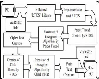
Figure.4: Work flow using Xilkernal
Fig 4 shows the total work flow using RTOS (Xilkernal).Presently FPGAs are considered as a major platform for high performance embedded applications as it provides the opportunity for reconfiguration as well as good clock speed and design resources. In present day application scenarios most embedded systems have real-time requirements that demand the use of Real-real-time operating systems (RTOS), which creates a suitable environment for real time applications to be designed and expanded easily. In an RTOS the design process is simplified by splitting the application code into separate tasks and then the scheduler executes them according to a specific schedule, meeting the real-time deadline.
The merit of our paper lies in the implementation of cryptographic algorithm utilizing threads, run by an RTOS on FPGA systems, which is quite challenging in this reconfigurable architecture domain. The usage of RTOS is advantageous in many respects, as RTOS is an efficient tool to optimize the software runtime as the code complexity grows, by distributing the tasks into multiple threads. Better and safer synchronization and resource management are also major advantages of an RTOS. As an RTOS, we have chosen Xilkernal. Below figure shows the exact communication between FPGA’s.[11]-[12].
Figure.5: Communication between two FPGAs using RTOS
IV. RESULTS
The Fig 5 shows the hardware configuration for communication between two FPGA’s. In this communication we require two PC’s two FPGA’s and three RS-232 cables. RS232 (DTE to DCE cable) is used for communication between FPGA and PC. RS232 (DTE to DTE cable) is used for communication between two FPGA’s. It is used to transfer data from one FPGA to another FPGA.
The two different cables and its connections with FPGAs are shown in the Fig 6.
Figure.6: Test setup
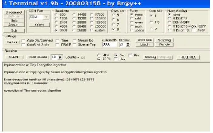
The below figure shows the print statements in terminal software from Transmitter section while running the ‘C’ code from SDK. The terminal having the settings such as com1 for serial transmission of data with 9600 baud rate and other settings as shown. Here the maximum 8 characters as input are given along with 16 characters encryption key.
Figure.8: Output from Receiver end
The Fig 7 and Fig 8 shows the print statements in terminal software from Receiver section while running the ‘C’ code from SDK. So at the Receiver end, encrypted data is decrypted if the decryption key is correct.
Table 1.DEVICE UTILIZATION SUMMARY Number of Slices 4180 out of 4656 89% Number of Slice Flip
Flops 5427 out of 9312 58% Number of 4 input LUTs 5643 out of 9312 60% Number of bonded IOBs 93 out of 232 40% Number of BRAMs 15 out of 20 75%
Number of MULT18X18SIOs 3 out of 20 15% Number of GCLK 7 out of 24 29% Number of DCMs 2 out of 4 50% V. CONCLUSIONS
RTOS enables the effective management of multi threads exist in the system especially on configurable processor platform. RTOS enabled MicroBlaze soft core processor is implemented to provide communication between two FPGA’s (chip to chip communication) in secured manner by applying tiny encryption algorithm on FPGA.
VI. REFERENCES
[1] S. Sau , C. Pal and A Chakrabarti "Design and Implementation of Real Time Secured RS232 Link for Multiple FPGA Communication, Proc. Of International Conference on Communication, Computing & Security,201 I, ISBN - 978-1-4503-0464-1.
[2] C. D. Walter. August 1999. Montgomery's Multiplication Technique: How to Make It Smaller and Faster. Cryptographic Hardware and Embedded Systems, Lecture Notes in Computer Science, Springer. No. 1717. pp. 80-93.
[3] A Mazzeo, L. Romano, G. P. Saggese and N. Mazzocca. 2003. FPGABased Implementation ofa Serial RSA Processor. Design. Proceedings of the conference on Design, Automation and Test in Europe - Volume I. ISBN:O-7695-1870-2.
[4] xilkernel_v3.00.pdf on www.xilinx.com.
[5] R. L. Rivest et al. 1978. A Method for Obtaining Digital Signatures and Public-Key Cryptosystems. Communications of the ACM. Vol. 21. pp. 120-126. [6] Cryptography & Network Security By Behrouz AForouzan.
[7] Montgomery Algorithm for Modular Multiplication Professor Dr. D. J. Guan ,August 25, 2003.
[8]RSA & Public Key Cryptography in FPGAs, John Fry, Martin Langhammer Altera Corporation -Europe [9] A. Tenca, C. Koc. 1999. A Scalable Architecture for Montgomery Multiplication. Cryptographic Hardware and Embedded Systems, Lecture Notes in Computer Science, No. 1717, pp. 94-108.
[10]. A. Tenca, G. Todorov, C. Koc. May 2001. High-radix design of a scalable modular multiplier. Cryptographic Hardware and Embedded Systems, Lecture Notes in Computer Science, Springer. No. 2162. pp. 185-201.
[11] High-Speed RSA Implementation, Cetin Kaya Koc, November 1994, Version 2.0, ftp://ftp.rsa.comlpub/pdfs/tr20I.pdf.
[12] http://csrc.nist.gov/publications/fips/fipsI97Ifips-197.pdf.
AUTHORS:
P.SUMATHA, Received B.Tech Degree
in Electronics and Communication Engineering in 2007 and presently pursuing M. Tech VLSI Design in Aurora's Research & Technological Institute, Warangal, INDIA.
B.PRASANNAJYOTHI, Working as
Associate Professor, Dept of ECE, Aurora's Research & Technological
Institute, Warangal, INDIA. She received M.Tech Degree from Ramappa Engineering College, JNTUH, INDIA.
CH. MADHAN MOHAN, Working as a Application Engineer at Unistring Tech Solutions, Hyderabad. He received M.Tech Degree from JBIT, Hyderabad, INDIA.