Joule Heating Effect on Field-Free Magnetization Switching by Spin-Orbit Torque
in Exchange-Biased Systems
Seyed Armin Razavi,1 Di Wu,1,2 Guoqiang Yu,1,*Yong-Chang Lau,3 Kin L. Wong,1 Weihua Zhu,2 Congli He,1 Zongzhi Zhang,2 J. M. D. Coey,3 Plamen Stamenov,3Pedram Khalili Amiri,1,4 and Kang L. Wang1
1Department of Electrical Engineering, University of California,
Los Angeles, California 90095-1594, USA
2Key Laboratory of Micro and Nano Photonic Structures (Ministry of Education),
Department of Optical Science and Engineering, Fudan University, Shanghai 200433, People’s Republic of China
3
CRANN, AMBER and School of Physics, Trinity College Dublin, Dublin 2, Ireland
4Inston Inc., Los Angeles, California 90095, USA
(Received 27 September 2016; revised manuscript received 20 January 2017; published 23 February 2017)
Switching of magnetization via spin-orbit torque provides an efficient alternative for nonvolatile memory and logic devices. However, to achieve deterministic switching of perpendicular magnetization, an external magnetic field collinear with the current is usually required, which makes these devices inappropriate for practical applications. In this work, we examine the current-induced magnetization switching in a perpendicularly magnetized exchange-biased Pt=CoFe=IrMn system. A magnetic field annealing technique is used to introduce in-plane exchange biases, which are quantitatively characterized. Under proper conditions, field-free current-driven switching is achieved. We study the Joule heating effect, and we show how it can decrease the in-plane exchange bias and degrade the field-free switching. Furthermore, we discuss that the exchange-bias training effect can have similar effects.
DOI:10.1103/PhysRevApplied.7.024023
I. INTRODUCTION
Spin-orbit torque (SOT) switching of magnetization is a promising emerging technology for memory and logic applications[1–3], which offers an advantage over conven-tional spin-transfer torque in terms of dynamic power dissipation[4–6]. However, to achieve high bit densities, perpendicular magnetization is required[7]. Switching of perpendicular magnetization by SOT has been widely investigated; when an in-plane charge current is passed through a material with high-spin-orbit coupling, such as a heavy-metal layer (Pt [1,3,8], Ta [9–11], W [12], and Hf [13,14]) or even a topological insulator [15], a spin current is generated, and it can apply torques on the adjacent ferromagnetic layer[3,8,16–18]. However, deter-ministic switching of perpendicular magnetization driven by SOT requires an additional inversion symmetry breaking
[19]. Usually, this symmetry is broken by applying an external magnetic field collinear with the current, which is impractical in device applications.
There have been efforts to achieve deterministic switch-ing without the need of an external field. Field-free switching has been achieved by introducing a lateral structural asymmetry, where the thickness of one layer is changed laterally [10,19,20] or by inducing a tilt in the
uniaxial anisotropy axis [21]. More recently, field-free switching was realized in the antiferromagnet and ferro-magnet systems, where some form of in-plane exchange bias (EB) is used instead of an external field[22–25].
In this work, we use a technique for magnetic field annealing based on current-induced Joule heating and a method for in-plane EB characterization based on measure-ment of the anomalous Hall effect. With the help of these techniques, we study the field-free switching in the exchange-biased films with the core structure of Pt=CoFe=IrMn. The in-plane EB at the interface of CoFe and IrMn replaces the external field and leads to determin-istic field-free switching. By examining the in-plane EB on the device level, we characterize the Joule heating and EB training effects in these structures. We discuss how these effects reduce the in-plane EB field over several switching cycles and, hence, degrade the field-free switching. The results may find potential applications in SOT devices.
II. SAMPLE PREPARATION AND MAGNETIC CHARACTERIZATIONS
The samples consisting of Tað2Þ=Ptð3Þ=CoFeð0.9; 1.1Þ= IrMnð3Þ=Ptð1Þ (thicknesses in nanometers) are grown on Si=SiO2 substrates by dc magnetron sputtering at room temperature. The samples are patterned into an array of Hall bar devices by standard photolithography and dry-etching techniques. The Hall bars have dimensions of 20×130μm2 and 10×40μm2. These devices are
*
measured using a Keithley 6221 current source, a Keithley 2182A nanovoltmeter, and a Stanford Research Systems SR830 lock-in amplifier. For low-temperature measure-ments, we use a physical-properties measurement system. The external magnetic field is generated by an electromag-net driven by a Kepco power supply. All measurements are carried out at room temperature, unless specified. All the magnetic characterizations are done on the device level in order to be more consistent with the rest of the results. The resistance characterizations are carried out using four-probe measurements. Similar results are also obtained in several batches of the same structures.
The current-driven field-free switching mechanism is depicted in Fig.1(a). A charge current passing through Pt generates a spin current via the spin Hall effect, and the resulting spin current exerts torques on the magnetization of the CoFe layer. The schematic of the measurement is
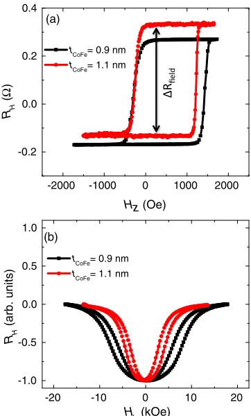
depicted in Fig.1(b). The magnetic properties characterized by anomalous Hall measurement are shown in Fig.2. Here, the samples are annealed with an out-of-plane magnetic field of 1 T for 10 min in the−Z direction. Figures 2(a)
and2(b)show anomalous Hall resistance as a function of out-of-plane and in-plane magnetic fields, respectively. In Fig. 2(a), the difference between the resistances of two states is defined by ΔRfield, which represents the total change in perpendicular magnetization measured by the anomalous Hall effect when an out-of-plane external magnetic field is used to switch the magnetization. Perpendicular magnetic anisotropy and out-of-plane EB are present in both samples. The small hysteresis loops in Fig. 2(b) may be a result of misalignment between the external in-plane field and the film’s surface. It should also be noted that because of the EB in Fig.2(b), the samples do not switch between the two stable states along the easy axis, only one of the up or down states is observed. As expected, the sample withtCoFe¼0.9nm has a larger EB because of its thinner ferromagnetic layer[26]. However, the sample with tCoFe¼1.1nm switches at lower critical current densities, which should be more appropriate for field-free
FIG. 1. (a) The studied structure for field-free switching. An antiferromagnet is placed on top of the ferromagnetic layer with perpendicular magnetic anisotropy. A spin current is generated in Pt and exerts torques on the magnetization of the ferromagnetic layer. The in-plane exchange biasHIPEBreplaces the external field
for field-free switching. (b) Schematic of the measurement.Iand
V show the applied current direction and the measured voltage, respectively. The direction of the exchange-bias field is either out of plane along Zˆ or in the longitudinal directionLˆ. For all the measurements, a Hall bar is used. For current-driven switching measurements, an external magnetic field is applied along the current direction Lˆ. Hall voltage is induced by a current I of constant amplitude 0.5 mA, which is then converted to Hall resistance.M is the magnetization direction, andθandφare its polar and azimuthal angles.
(b) (a)
-0.2 0.0 0.2 0.4
RH
(
Ω
)
Hz (Oe) tCoFe= 0.9 nm
tCoFe= 1.1 nm
-2000 -1000 0 1000 2000
-20 -10 0 10 20
-1.0 -0.5 0.0 0.5 1.0
RH
(arb.
units)
[image:2.612.92.252.270.537.2]HL (kOe) tCoFe= 0.9 nm tCoFe= 1.1 nm
[image:2.612.347.528.327.627.2]switching since the Joule heating effects are relatively smaller. We also try CoFe layers thinner than 0.9 nm, but as expected, they have even larger critical switching currents and, consequently, a more pronounced Joule heating effect. Furthermore, the samples with CoFe layers thicker than 1.1 nm do not have a good perpendicular magnetic anisotropy and are not useful for the applications. As we discuss in Sec. V, the Joule heating effects are found to degrade the field-free switching; hence, for all the switch-ing measurements, we use the sample withtCoFe¼1.1nm.
III. CURRENT-DRIVEN MAGNETIZATION SWITCHING WITH OUT-OF-PLANE
EXCHANGE BIAS
We first discuss the current-driven switching in the presence of an out-of-plane EB to show the possibility of switching by SOT and to show that out-of-plane EB does not result in field-free switching. A harmonic technique is used to investigate the current-induced SOTs in this case
[16,18,27]. It should be noted that in this device,
ξ≡ΔRP=ΔRA¼0.12, which is the ratio between the planar Hall effect and anomalous Hall effect resistances. To measureΔRP (planar Hall effect resistance), a large in-plane field of 1.5 T is applied to the sample to make the magnetization in plane. Then, the transverse resistance is measured as a function of the angle between the in-plane field and the current direction. ΔRP is defined as the difference between the maximum and the minimum values of the transverse resistance. Furthermore,ΔRA(anomalous Hall resistance) is defined in the same way asΔRfieldshown in Fig. 2(a). For the harmonic measurements, a small ac current is passed through the current channel in the presence of an in-plane magnetic field applied along the
current (voltage) channel for measuring dampinglike (field-like) fields. The ratios corresponding to dampinglike (BL) and fieldlike (BT) torques are then calculated[27]
BLðTÞ ¼−2
∂V2ω
∂HLðTÞ
=
∂2V
ω
∂H2
LðTÞ
; ð1Þ
where Vω and V2ω are the first- and second-harmonic anomalous Hall voltage signals, respectively. Figures 3(a)–3(d) show the results for the first- and sec-ond-harmonic measurements, which are fitted by parabolic and linear functions, respectively. Finally, we can obtain the dampinglike (ΔHL) and fieldlike (ΔHT) fields[27]
ΔHL¼ ðBL2ξBTÞ=ð1−4ξ2Þ;
ΔHT ¼ ðBT2ξBLÞ=ð1−4ξ2Þ; ð2Þ
where due to our measurement configuration, we use the positive sign in the numerator. Figure3(e)shows the fieldlike and dampinglike fields at different peak currents. In the small-current regime, the effective fields have a linear dependence on the applied current. Based on the resistances of each layer, the portion of current flowing through the Pt layer is calculated. We estimate that about 47% of the total current passes through the Pt layer. Therefore, the effective dampinglike and fieldlike field efficiencies (ΔHLðTÞ=J) are calculated to be 22.31 and 7.04 Oe per107A=ðcmÞ2, respectively, where J is the peak current density passing through Pt. These values are slightly smaller than other reported values[28,29]. This can be due to the fact that a much smaller portion of the current passes through the IrMn layer, which also generates SOT, and its torques tend to partially cancel the torques from the Pt layer, since they have
(b) (a)
(d) (c)
(e)
-1 0 1
-1.656 -1.644
V
(mV
)
H (kOe) Transverse
-1 0 1
-0.24 -0.16
V2
(
μV)
HT (kOe)
0.0 3.0x10⁶ 6.0x10⁶ 9.0x10⁶
-12 -9 -6 -3 0
Δ
H
(Oe
)
JPt (A/cm2)
ΔHT
ΔHL
-1 0 1
-1.725 -1.710
Vω
ω
ω ω
(mV
)
HL (kOe) Longitudinal
-1 0 1
-0.4 -0.2 0.0
V2
(
μ
V)
[image:3.612.93.519.483.663.2]HL (kOe) T
the same sign of the spin Hall angle[30]. It should be noted that the SOT responsible for switching stems from the Pt layer rather than IrMn because of its much higher current density. Assuming that the dampinglike torque is a result of the spin Hall effect solely, we can find the spin Hall angle usingθSHE¼ ð−2jejMstF=hÞ×ðΔHL=JÞ, wherejej,h,tF, and Ms represent the absolute value of the electron’s charge, Planck’s constant, ferromagnetic layer thickness, and the saturation magnetization of the ferromagnetic layer
[31]. Using a superconducting quantum-interference-device measurement, the saturation magnetization is found to be 1100emu=cm3. The obtained spin Hall angle for Pt in this structure is 0.082, which is similar to the other reported values for Pt[32].
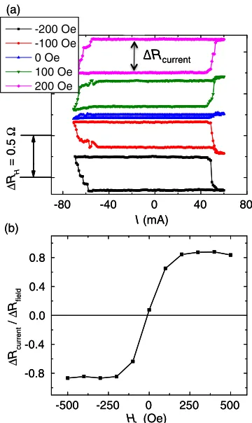
In order to achieve deterministic switching, we need to break the inversion symmetry; thus, as expected, the out-of-plane EB does not result in field-free switching. Anomalous Hall resistance is used for current-driven switching characterization, and the measurement setup is depicted in Fig.1(b). For the switching measurement, first an initialization current pulse ofþ60mA is applied to the sample. Then, the applied current is swept from þ60 to −70mA and back toþ60mA in the presence of different in-plane magnetic fields, which are collinear with the current direction. To make the switching measurements consistent with the other switching measurements in this work, pulses with 200μs widths and a 1-s wait between successive pulses are used to drive the magnetization switching.
The resulting plots are shown in Fig.4. The anomalous Hall resistance is proportional to the perpendicular mag-netization; thus, in order to better describe the current-driven switching under different in-plane magnetic fields, we look at the total change in anomalous Hall resistance after sweeping the current.ΔRfieldðΔRcurrentÞrepresents the total perpendicular magnetization reversal when an out-of-plane field (current) is swept. In this case, ΔRfield¼ 0.473Ω. As can be seen in Fig. 4(a), ΔRcurrent is almost negligible for the zero-field case, which indeed shows that there is no field-free switching. Applying negative and positive in-plane fields results in different switching polarities because of the opposite SOT directions [3]; however, jΔRcurrentj is symmetric around the zero field, in other words, there is no shift in the switching diagram, which is reasonable since the EB direction is out of plane. The switching diagram is plotted in Fig.4(b). The vertical axis showsΔRcurrent=ΔRfield, which is plotted as a function of different external in-plane magnetic fields HL. ΔRcurrent=ΔRfield represents the switching percentage of the sample’s area as a result of applying current detected by the anomalous Hall effect. In our notations,ΔRcurrenthas a positive (negative) value if at large positive currents the state with positive (negative) anomalous Hall resistance is preferred. Thus, positive and negative values of ΔRcurrent correspond to different switching polarities. In this case, we
do not have field-free switching; the very small shift in the switching diagram is negligible and may be due to the remanent in-plane field of the magnet.
As can be seen in Fig. 4(b), ΔRcurrent does not reach
0.473Ω, even in the presence of larger in-plane magnetic fields. We suppose this is due to the fact that the current density becomes smaller on the Hall bar cross-section area and does not reach the critical value. Furthermore, the additional pinning effect at the cross-section area may make complete switching difficult[30]. Hence, the cross-section region of the device is not completely switched, and ΔRcurrent does not reach ΔRfield.
IV. FIELD-FREE MAGNETIZATION SWITCHING WITH IN-PLANE EXCHANGE BIAS
A. In-plane exchange-bias measurement
For field-free perpendicular magnetization switching, an in-plane EB needs to be introduced. For this purpose, the
(a)
Rcurrent
(b)
Δ
RH
= 0.5
Ω
I (mA)
-200 Oe -100 Oe 0 Oe 100 Oe 200 Oe
-80 -40 0 40 80
-500 -250 0 250 500
-0.8 -0.4 0.0 0.4 0.8
Δ
Rcurr
ent
/
Δ
Rfie
ld
HL (Oe)
(a)
Rcurrent
(b)
Δ
RH
= 0.5
Ω
I (mA)
-200 Oe -100 Oe 0 Oe 100 Oe 200 Oe
-80 -40 0 40 80
-500 -250 0 250 500
-0.8 -0.4 0.0 0.4 0.8
Δ
Rcurr
ent
/
Δ
Rfie
ld
[image:4.612.347.527.44.346.2]HL (Oe)
FIG. 4. (a) Current-driven switching in the sample with out-of-plane EB in the presence of different external in-plane magnetic fieldsHL. No asymmetry injΔRcurrentjbetween positive and negative magnetic field values is observed. A current of 45 mA corresponds to a current density of approximately
sample’s temperature should be raised above the blocking temperature in the presence of a large in-plane magnetic field. The blocking temperature is defined as the lowest temperature at which the exchange bias becomes zero[26]. In order to extract the blocking temperature quantitatively, we measure the temperature dependence of the out-of-plane EB. First, the sample is annealed with an out-of-plane field. Then, its temperature is reduced to 100 K in vacuum and in the presence of an out-of-plane field of 1 T. Subsequently, the out-of-plane EB is measured at different temperatures up to 350 K, and by fitting the data, the blocking temper-ature is found to be around 360 K.
We anneal the devices using current-induced Joule heating in the presence of a large in-plane magnetic field, which can saturate the magnetization. In this technique, a dc current with proper amplitude is applied to the device, which is placed inside a magnetic field. The amplitude of the applied current is large enough to raise the sample’s temperature above the blocking temperature but not to burn the device. The appropriate amplitude is found experimen-tally for each CoFe thickness. The magnetic field is applied along the longitudinal direction of the Hall bar; hence, the longitudinal EB is obtained in theLdirection as shown in Fig. 1(b). For the sample with tCoFe¼1.1nm, we apply 20- and 30-mA dc currents for the 10- and20-μm Hall bar widths, respectively, which translates to a temperature of 400 K according to the temperature dependence of the resistance in the sample. This temperature is indeed higher than the blocking temperature. This amplitude results in the largest in-plane EB without damaging the structure. The current is applied for 10 min in the presence of an external field of 1.5 T. Then the samples are cooled for 5 min in the air with the magnetic field on. After this procedure, the samples have the same total resistance change ΔRfield measured by anomalous Hall effect, which suggests that the magnetic properties are not degraded.
In order to measure the in-plane EB field, the anomalous Hall resistance is measured as a function of in-plane external field. The total magnetic energy can be expressed as
E¼ ð−Kuþ2πM2sÞcos2θ
−MsðHTcosφsinθþHLsinφsinθþHzcosθÞ;
ð3Þ
where Ku is the magnetic anisotropy, which is in out-of-plane direction,Msis the saturation magnetization, θand
φare the polar and azimuthal angles of the magnetization, respectively, and HT, HL, and Hz are the transverse, longitudinal, and perpendicular magnetic field compo-nents, respectively, as illustrated in Fig. 1(b). It should be noted that here we assume that the magnetization remains uniform in the process. For the in-plane EB measurement, an external field in the longitudinal
direction is applied, hence, φ¼90°. Thus, Eq. (3) can be rewritten as
E¼ ð−Kuþ2πM2
sÞcos2θ−MsH0Lsinθ; ð4Þ
whereH0L¼HLþHIP
EB should be used instead of HL to account for the in-plane EB field. Here, we assume that the out-of-plane EB is small and negligible, which can be confirmed by the out-of-plane AHE loop. For different values of external magnetic field, the total energy should be minimized with respect to θ. As a result,
∂E
∂θ¼ ð−Kuþ2πM2sÞð−sin2θÞ−MsH0Lcosθ¼0. ð5Þ
SinceH0Lis small compared to the anisotropy field, then cosθ¼0is not a physically valid solution. Thus,
sinθ¼ MsH 0 L
2ðKu−2πM2sÞ¼αH
0
L; ð6Þ
where αH0L is very small, and α is a constant for each sample. The anomalous Hall resistance is proportional to the out-of-plane component of the magnetization orRH ∝ Mz¼Mcosθ¼M
ffiffiffiffiffiffiffiffiffiffiffiffiffiffiffiffiffiffiffiffiffiffiffi
1−ðαH0
LÞ2
p
, which can be approxi-mated near αH0L ¼0 as RH ∝M½1−ðα2H0L2=2Þ ¼ M½1−ðα2=2ÞðH
LþHIPEBÞ2. Consequently, in order to find the EB field,RHis measured at multiple in-plane magnetic fields around its extremum, then a quadratic function is fitted, and the extremum value is found. The extremum is where H0L¼HLþHIP
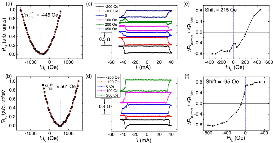
EB¼0, so the EB field can be extracted. This is illustrated in Figs.5(a)and5(b). On the same structure as in Sec.III(tCoFe¼1.1 nm), an in-plane EB field is introduced in two opposite directionsLˆ. A small current of 0.5-mA amplitude is used to measure the anomalous Hall resistance, and the EB fields are extracted using the method described above. In this measurement, the in-plane magnetic field is swept back and forth, and each point on the graph represents the average of the two values. The difference of the EB magnitudes for the opposite directions comes from the fact that they are measured on two different devices. However, these devices both have the same structure and are from the same film; thus, this small difference does not affect the validity of the arguments.
This method enables us to quantitatively measure the in-plane EB at different stages in the process. Hence, we are able to do a comprehensive study of the Joule heating and training effects on the in-plane EB and field-free switching, which are discussed in more detail in Sec.V.
B. Field-free magnetization switching
described in the following. The measurement is done as described in Sec. III. Again, for these measurements, a pulsed current is used. The results are depicted in Figs.5(c)
and 5(d), where field-free switching is observed as expected. The field-field switching polarity with positive (negative) EB field is the same as that with positive (negative) external in-plane field, which indicates that the in-plane EB indeed plays the role of the external field. Unlike Fig. 4(a), in this case jΔRcurrentj is asymmetric with respect to different in-plane magnetic fieldsHL. We attribute this phenomenon to the presence of in-plane EB. Switching diagrams are plotted in Figs. 5(e) and 5(f). A clear shift in two different directions is observed, which is consistent with the EB field directions for each case. As a result of these shifts, field-free switching is achieved. This can be described very well with the depicted switching diagrams; in these cases,ΔRcurrentis large at zero field but vanishes at some other in-plane field, where the EB cancels the external field, and no switching is observed. In these switching diagrams,ΔRcurrent andΔRfield at zero field are around 50% and 90% of the maximum values, respectively. The maximum value of 0.81 is obtained for an approx-imately 400-Oe in-plane field.
It should be noted that in both cases, the shift in the switching diagram is smaller than the measured in-plane EB field. As we discuss in more detail in Sec.V, this can be a result of the nonuniformity of the EB field throughout the
device[22]or the in-plane EB reduction because of Joule heating or EB training effect [33]. However, this needs further investigation. Furthermore, the amount of shift in Figs.5(e)and5(f)is not the same. This may be due to Joule heating or the EB training effect, which can change the in-plane EB during the measurement, and, consequently, the observed shifts in the switching diagrams depend on the sequence in which the measurement is carried out.
V. JOULE HEATING AND EXCHANGE-BIAS TRAINING EFFECTS ON THE
FIELD-FREE SWITCHING
A. Joule heating effect
In order to limit the heating effects in the current-driven switching measurements, a pulsed current is used. The critical current for switching is around 40–50 mA, depend-ing on the device dimensions, which translates to a current density of approximately4×107A=cm2passing through the Pt layer. These relatively large amplitudes can increase the sample’s temperature through Joule heating. The IrMn thickness of the structure used in the measurements is 3 nm; thus, a low blocking temperature is expected[34].
For a quantitative study of the Joule heating effects, we measure how the temperature of the sample changes in the switching measurement. To that end, we measure how the resistance of the sample changes during the time that the
(a)
(b)
(e) (c)
(f) (d)
-1000 0 1000 0.0
0.2 0.4 0.6 0.8 1.0
RH
(arb. un
it
s)
HL (Oe)
HEBIP = -445 Oe
-1000 0 1000 0.0
0.2 0.4 0.6 0.8 1.0
RH
(arb. units)
HL (Oe)
HEBIP = 561 Oe
-60 -40 -20 0 20 40
I (mA)
-200 Oe -100 Oe 0 100 Oe 200 Oe 450 Oe
0.5 Ω
-60 -40 -20 0 20 40
I (mA)
-200 Oe -100 Oe 0 Oe 100 Oe 200 Oe
0.4 Ω
-400 -200 0 200 400 600 -0.8
-0.4 0.0 0.4 0.8
Δ
Rcur
ren
t
/
Δ
Rfie
ld
HL (Oe)
Shift = 215 Oe
-800 -400 0 400 -0.8
-0.4 0.0 0.4 0.8
Δ
Rcurrent
/
Δ
Rfield
HL (Oe)
[image:6.612.85.525.45.276.2]Shift = -95 Oe
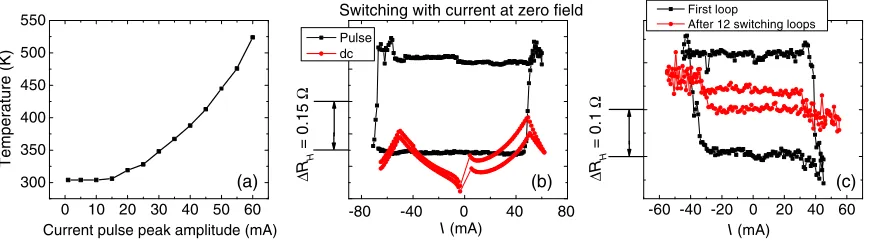
pulses are applied for switching. We also measure the temperature dependence of resistance, in a range from 110 to 350 K, and we extrapolate the resistance at higher temperatures. By comparing these two sets of data, we estimate the temperature changes during switching. As can be seen in Fig. 6(a), the temperature can rise to 500 K during the switching, which is well above the blocking temperature. This can result in an irreversible loss of the exchange bias.
In order to show the importance of the heating effects in these structures, we compare the field-free switching of a sample under pulsed and dc currents. For the dc current measurement, which is an extreme case in terms of Joule heating, the amplitude of the applied current changes from large negative values to large positive values and back with no delay between consecutive values. Each value is applied for around 200 ms.
For this purpose, a sample with tCoFe¼1.1nm is annealed using the current. An in-plane EB field of 540 Oe is introduced in the sample. Then the sample is switched using dc current at zero external field. Afterwards, the annealing procedure is repeated to ensure that the in-plane EB field of 540 Oe is still present. This time, the sample is switched at zero external field using pulsed current. The results are shown in Fig. 6(b). With pulsed current, field-free switching is achieved, while with dc current, almost no change in Hall resistance (or, equiv-alently, in perpendicular magnetization) is observed. We attribute this effect to Joule heating and its impact on the disappearance of the in-plane EB, since the temperature of the sample rises above the blocking temperature during the measurement.
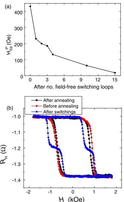
Furthermore, even if pulsed current is used, the field-free switching still degrades after repeating the measurement several times. This can be seen in Fig.6(c). Here, the field-free switching measurement of the same structure used above is repeated 12 times. The total change in Hall resistance in the switching measurement is decreased,
and the field-free switching disappears over the time. This can again be attributed to the Joule heating effect. However, in this case, the EB training effect may also be a contributing factor, and this is discussed in the next section. With the help of our device-level in-plane EB measure-ment technique, we observe that after each current-driven field-free switching cycle, the in-plane EB is reduced and eventually it disappears, as depicted in Fig.7(a). As noted, in the switching measurement, the temperature of the sample goes above the blocking temperature during the pulse application time. On the other hand, the relevant time scaleτfor antiferromagnetic reordering is given by[22,35]
1
τ¼ν0exp
− Eb kBT
; ð7Þ
whereν0≈109Hz is the attempt frequency,Ebis the energy barrier for antiferromagnetic grain reversal, kB is Boltzmann’s constant, andTis the temperature. For samples with several weeks of stability,τ is around 106 s at room temperature (T0), which results in Eb≈34.5×kBT0. The temperature in our measurement goes as high as 500 K, so the corresponding time scale τ is approximately 1 s, which is much longer than the pulse duration of 200 μs. Consequently, the exchange bias does not vanish with one large pulse; it decreases gradually after many pulses. This can also explain why in the dc measurement no field-free switching is observed. In the dc measurement, the high temperature is kept for much longer than 1 s; as a result, the exchange bias vanishes instantly, and no field-free switching is observed. It should be noted that the Joule heating of the 0.1-mA current used for in-plane EB measurement is found to be negligible based on a control measurement in which only the current is applied. In the control measurement, the sample is not switched; only an in-plane field is applied to measure the in-in-plane EB succes-sively, and after 20 times, there is no significant change in the
(b) (c)
) a (
0 10 20 30 40 50 60 300
350 400 450 500 550
Temperature (K)
Current pulse peak amplitude (mA)
-60 -40 -20 0 20 40 60
Δ
RH
=
0.1
I (mA)
First loop
After 12 switching loops
-80 -40 0 40 80
I (mA)
Pulse dc
Switching with current at zero field
Δ
RH
=
0.15
[image:7.612.91.528.533.655.2]Ω Ω
EB value. This shows that the heating effect of the 0.1-mA current can be neglected.
The disappearance of in-plane EB as a result of heating can be further supported by the comparison of anomalous Hall data,RH as a function ofHz, at different stages in the process: before and after current annealing with in-plane field and after the current-driven switching measurement shown in Fig. 7(b). After annealing in the presence of a large in-plane magnetic field, the out-of-plane EB decreases, which shows that the pinning is in the in-plane direction. Also, the coercivity is decreased by approxi-mately 100 Oe when the out-of-plane EB decreases, which agrees with other reported findings [36]. After annealing, current is used to switch the sample through 12 cycles, where the critical current for switching is around 45 mA. After current-driven switching measurement, the out-of-plane EB appears again, this time in the form of double loops, which further indicates the presence of heating
effects. The temperature of the sample with perpendicular easy axis is raised above the blocking temperature in the course of the switching measurement in the absence of any large external fields. Consequently, the out-of-plane EB tends to appear again, but there is no preference between upward and downward pinning directions because both are along the easy axis, and there is no external field to make a preference. Thus, some parts of the sample have an upward pinning and the other parts have a downward pinning; hence, the double-loop EB appears.
Increasing the IrMn thickness raises the Néel and blocking temperatures; however, that is not desirable since it also increases the shunting effect. The SOT for switching stems from the Pt layer, as shown in Sec.III. By increasing the IrMn thickness, the shunting effect becomes significant and less current passes through Pt. Consequently, the critical current for switching increases. This results in more Joule heating effect and is not desirable. We try samples with thicker IrMn layers up to 10 nm, but field-free switching is not achieved in them.
The Joule heating effect is helpful when switching is assisted with an external in-plane field. In the same sample, using dc current reduces the critical current density for switching by 10% compared to the case where pulsed current is used. That is due to the fact that the Joule heating effect raises the temperature of the sample and reduces the anisotropy, and, consequently, switching becomes easier. On the other hand, when an in-plane EB is used for field-free switching, the heating effect is no longer desirable, since it reduces the in-plane EB field. In this case, avoiding the thermal effect is crucial.
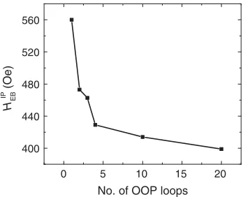
B. Exchange-bias training effect
Even if very short pulses with negligible heating effects are used, the in-plane EB will not be constant after successive switchings due to the EB training effect. The training has mostly been investigated in cases where an external magnetic field is used for cycling through hyste-resis loops[33,37,38]. However, it can also exist when SOT is used for magnetization switching. The spin structure at the interface of the antiferromagnet and ferromagnet deviates from its equilibrium state when an EB field is created. Consecutive switchings can result in a rearrange-ment of the IrMn’s spin structure at the interface of IrMn= CoFe towards an equilibrium state [33]. Consequently, a gradual decrease in the in-plane EB is possible. It should be noted that there are also some other models and explanations provided for the origin of the EB training effect[38–43]. However, in this work, we focus only on the general concept.
In order to show this effect in our structure, a sample with tCoFe¼1.1nm is current annealed, and an in-plane EB field of 560 Oe is introduced. Then, an out-of-plane external field is used to switch the sample back and forth. Afterwards, the in-plane EB is measured again and so on.
(a)
(b)
0 3 6 9 12 15
0 100 200 300 400
HEB
IP (Oe)
After no. field-free switching loops
-2 -1 0 1 2
-1.4 -1.3 -1.2 -1.1 -1.0
RH
(
Ω
)
Hz (kOe)
[image:8.612.79.276.42.363.2]After annealing Before annealing After switchings
The result is depicted in Fig. 8. After each out-of-plane loop, the in-plane EB is decreased, and this can be attributed to the training effect. In our case, SOT is used to switch the perpendicular magnetization. However, as described above, multiple switchings of the magnetization itself result in a reduction of the in-plane EB. This can be a major problem for these devices, since the in-plane EB is essential for field-free switching. As shown in Fig.8, after only 20 successive switchings, the in-plane EB is reduced by around 30%. This effect will deteriorate the device performance very fast over the time. By comparing the results of Figs. 7 and 8, it can be seen that in our measurements, the Joule heating effect is dominant over the exchange-bias training effect in terms of decreasing the in-plane EB.
VI. CONCLUSION
Field-free perpendicular magnetization switching driven by spin-orbit torque in an asymmetric exchange-biased system of Ta=Pt=CoFe=IrMn=Pt is achieved with the help of device-level magnetic field annealing. The induced in-plane EB plays the role of the external magnetic field required for breaking system symmetry. Through in-plane EB characterization techniques, it is found that Joule heating and exchange bias training effects can significantly affect the field-free switching in these structures. In order to make practical applications possible, these effects are very important issues that need to be addressed. To have more robust field-free switching, very narrow pulses can help with the Joule heating problem, as suggested by the comparison of dc and pulsed currents for switching, where a significant improvement can be seen with pulsed currents. Furthermore, a thin layer inserted between the ferromag-netic and antiferromagferromag-netic layers can help with thermal stability [22]. The training effect is known to be smaller in structures with single-crystalline antiferromagnet layers
[26]; thus, that may potentially help with the training-effect problem. Furthermore, as shown in Fig. 8, there is a saturation value for the in-plane EB, which can be high enough to be used for field-free switching. However, the training effect has to be studied in these devices, and they should be designed to have an adequate saturation value.
ACKNOWLEDGMENTS
This work is supported in part by C-SPIN and FAME, two of six centers of STARnet, a Semiconductor Research Corporation program sponsored by MARCO and DARPA. This work is also supported by the National Science Foundation (Grant No. ECCS 1611570) and Nanosystems Engineering Research Center for Translational Applications of Nanoscale Multiferroic Systems Cooperative Agreement Grant No. EEC-1160504. We like to acknowledge the collabo-ration of this research with the King Abdul-Aziz City for Science and Technology via The Center of Excellence for Green Nanotechnologies. This work is supported as part of the SHINES Center, an Energy Frontier Research Center funded by the U.S. Department of Energy, Office of Science, Basic Energy Sciences under Award No. S000686. D. W. and Z. Z. Z. thank for the support of the China Scholarship Council, the 973 Program (Grant No. 2014CB921104), and the National Natural Science Foundation of China Grant No. 11474067. Y.-C. L., P. S., and J. M. D. C. acknowledge the support by Science Foundation Ireland through AMBER and by Grant No. 13/ERC/I2561. In addition, G. Q. Y. acknowledges Junyang Chen for fruitful discussions.
S. A. R. and D. W. contributed equally to this work.
[1] I. M. Miron, K. Garello, G. Gaudin, P. J. Zermatten, M. V. Costache, S. Auffret, S. Bandiera, B. Rodmacq, A. Schuhl, and P. Gambardella, Perpendicular switching of a single ferromagnetic layer induced by in-plane current injection,
Nature (London)476, 189 (2011).
[2] L. Liu, C. F. Pai, Y. Li, H. W. Tseng, D. C. Ralph, and R. A. Buhrman, Spin-torque switching with the giant spin Hall effect of tantalum,Science336, 555 (2012).
[3] L. Liu, O. J. Lee, T. J. Gudmundsen, D. C. Ralph, and R. A. Buhrman, Current-Induced Switching of Perpendicularly Magnetized Magnetic Layers Using Spin Torque from the Spin Hall Effect,Phys. Rev. Lett.109, 096602 (2012). [4] R. Dorrance, J. G. Alzate, S. S. Cherepov, P. Upadhyaya,
I. N. Krivorotov, J. A. Katine, J. Langer, K. L. Wang, P. K. Amiri, and D. Marković, Diode-MTJ crossbar memory cell using voltage-induced unipolar switching for high-density MRAM,IEEE Electron Device Lett.34, 753 (2013). [5] K. L. Wang, J. G. Alzate, and P. K. Amiri, Low-power
non-volatile spintronic memory: STT-RAM and beyond,J. Phys. D46, 7 (2013).
[6] S. Ikeda, K. Miura, H. Yamamoto, K. Mizunuma, H. D. Gan, M. Endo, S. Kanai, J. Hayakawa, F. Matsukura, and
0 5 10 15 20
400 440 480 520 560
HEB IP (Oe)
[image:9.612.88.267.45.186.2]No. of OOP loops
H. Ohno, A perpendicular-anisotropy CoFeB-MgO mag-netic tunnel junction,Nat. Mater. 9, 721 (2010).
[7] S. Mangin, D. Ravelosona, J. A. Katine, M. J. Carey, B. D. Terris, and E. E. Fullerton, Current-induced magnetization reversal in nanopillars with perpendicular anisotropy,Nat.
Mater.5, 210 (2006).
[8] X. Qiu, K. Narayanapillai, Y. Wu, P. Deorani, D. H. Yang, W. S. Noh, J. H. Park, K. J. Lee, H. W. Lee, and H. Yang, Spin-orbit-torque engineering via oxygen manipulation,
Nat. Nanotechnol.10, 333 (2015).
[9] C. Zhang, S. Fukami, H. Sato, F. Matsukura, and H. Ohno, Spin-orbit torque induced magnetization switching in nano-scale Ta=CoFeB=MgO, Appl. Phys. Lett. 107, 012401 (2015).
[10] G. Yu, L. T. Chang, M. Akyol, P. Upadhyaya, C. He, X. Li, K. L. Wong, P. K. Amiri, and K. L. Wang, Current-driven perpendicular magnetization switching in Ta=CoFeB=
½TaOx or MgO=TaOx films with lateral structural asym-metry,Appl. Phys. Lett.105, 102411 (2014).
[11] C. O. Avci, K. Garello, C. Nistor, S. Godey, B. Ballesteros, A. Mugarza, A. Barla, M. Valvidares, E. Pellegrin, A. Ghosh, I. M. Miron, O. Boulle, S. Auffret, G. Gaudin, and P. Gambardella, Fieldlike and antidamping spin-orbit torques in as-grown and annealed Ta=CoFeB=MgO layers,
Phys. Rev. B89, 214419 (2014).
[12] C. F. Pai, L. Liu, Y. Li, H. W. Tseng, D. C. Ralph, and R. A. Buhrman, Spin transfer torque devices utilizing the giant spin Hall effect of tungsten,Appl. Phys. Lett.101, 122404 (2012).
[13] M. Akyol, G. Yu, J. G. Alzate, P. Upadhyaya, X. Li, K. L. Wong, A. Ekicibil, P. K. Amiri, and K. L. Wang, Current-induced spin-orbit torque switching of perpendicularly magnetized HfCoFeBjMgO and HfjCoFeBjTaOx struc-tures,Appl. Phys. Lett. 106, 162409 (2015).
[14] M. Akyol, J. G. Alzate, G. Yu, P. Upadhyaya, K. L. Wong, A. Ekicibil, P. K. Amiri, and K. L. Wang, Effect of the oxide layer on current-induced spin-orbit torques in HfCoFeBjMgO and HfjCoFeBjTaOx structures, Appl.
Phys. Lett.106, 032406 (2015).
[15] Y. Fan, P. Upadhyaya, X. Kou, M. Lang, S. Takei, Z. Wang, J. Tang, L. He, L. T. Chang, M. Montazeri, G. Yu, W. Jiang, T. Nie, R. N. Schwartz, Y. Tserkovnyak, and K. L. Wang, Magnetization switching through giant spin-orbit torque in a magnetically doped topological insulator heterostructure,
Nat. Mater.13, 699 (2014).
[16] J. Kim, J. Sinha, M. Hayashi, M. Yamanouchi, S. Fukami, T. Suzuki, S. Mitani, and H. Ohno, Layer thickness dependence of the current-induced effective field vector in TaCoFeBjMgO,Nat. Mater.12, 240 (2013).
[17] L. Liu, T. Moriyama, D. C. Ralph, and R. A. Buhrman, Spin-Torque Ferromagnetic Resonance Induced by the Spin Hall Effect,Phys. Rev. Lett.106, 036601 (2011). [18] K. Garello, I. M. Miron, C. O. Avci, F. Freimuth, Y.
Mokrousov, S. Blügel, S. Auffret, O. Boulle, G. Gaudin, and P. Gambardella, Symmetry and magnitude of spin-orbit torques in ferromagnetic heterostructures, Nat. Nanotech-nol.8, 587 (2013).
[19] G. Yu, P. Upadhyaya, Y. Fan, J. G. Alzate, W. Jiang, K. L. Wong, S. Takei, S. A. Bender, L. T. Chang, Y. Jiang, M. Lang, J. Tang, Y. Wang, Y. Tserkovnyak, P. K. Amiri, and
K. L. Wang, Switching of perpendicular magnetization by spin-orbit torques in the absence of external magnetic fields,
Nat. Nanotechnol.9, 548 (2014).
[20] G. Yu, M. Akyol, P. Upadhyaya, X. Li, C. He, Y. Fan, M. Montazeri, J. G. Alzate, M. Lang, K. L. Wong, P. K. Amiri, and K. L. Wang, Competing effect of spin-orbit torque terms on perpendicular magnetization switching in structures with multiple inversion asymmetries,Sci. Rep.6, 23956 (2016). [21] J. Torrejon, F. Garcia-Sanchez, T. Taniguchi, J. Sinha, S. Mitani, J. V. Kim, and M. Hayashi, Current-driven asym-metric magnetization switching in perpendicularly magnet-ized CoFeB=MgO heterostructures, Phys. Rev. B 91, 214434 (2015).
[22] A. v. d. Brink, G. Vermijs, A. Solignac, J. Koo, J. T. Kohlhepp, H. J. M. Swagten, and B. Koopmans, Field-free magnetization reversal by spin-Hall effect and exchange bias,Nat. Commun. 7, 10854 (2016).
[23] S. Fukami, C. Zhang, S. DuttaGupta, A. Kurenkov, and H. Ohno, Magnetization switching by spin-orbit torque in an antiferromagnet-ferromagnet bilayer system,Nat. Mater.15, 535 (2016).
[24] Y. C. Lau, D. Betto, K. Rode, J. M. D. Coey, and P. Stamenov, Spin-orbit torque switching without an external field using interlayer exchange coupling,Nat. Nanotechnol. 11, 758 (2016).
[25] Y. W. Oh, S. C. Baek, Y. M. Kim, H. Y. Lee, K. D. Lee, C. G. Yang, E. S. Park, K. S. Lee, K. W. Kim, G. Go, J. R. Jeong, B. C. Min, H. W. Lee, K. J. Lee, and B. G. Park, Field-free switching of perpendicular magnetization through spin-orbit torque in antiferromagnet/ferromagnet/ oxide structures,Nat. Nanotechnol.11, 858 (2016). [26] J. Nogués and I. K. Schuller, Exchange bias, J. Magn.
Magn. Mater.192, 203 (1999).
[27] M. Hayashi, J. Kim, M. Yamanouchi, and H. Ohno, Quantitative characterization of the spin-orbit torque using harmonic Hall voltage measurements, Phys. Rev. B 89, 144425 (2014).
[28] M. Yang, K. Cai, H. Ju, K. W. Edmonds, G. Yang, S. Liu, B. Li, B. Zhang, Y. Sheng, S. Wang, Y. Ji, and K. Wanga, Spin-orbit torque in Pt=CoNiCo=Pt symmetric devices,Sci. Rep.6, 20778 (2016).
[29] S. Emori, U. Bauer, S. Woo, and G. S. D. Beach, Large voltage-induced modification of spin-orbit torques in Pt=Co=GdOx,Appl. Phys. Lett.105, 222401 (2014). [30] D. Wu, G. Yu, C. T. Chen, S. A. Razavi, Q. Shao, X. Li, B.
Zhao, K. L. Wong, C. He, Z. Zhang, P. K. Amiri, and K. L. Wang, Spin-orbit torques in perpendicularly magnetized Ir22Mn78=Co20Fe60B20=MgO multilayer, Appl. Phys.
Lett.109, 222401 (2016).
[31] G. Yu, P. Upadhyaya, K. L. Wong, W. Jiang, J. G. Alzate, J. Tang, P. K. Amiri, and K. L. Wang, Magnetization switching through spin-Hall-effect-induced chiral domain wall propa-gation,Phys. Rev. B89, 104421 (2014).
[32] J.-C. Rojas-Sánchez, N. Reyren, P. Laczkowski, W. Savero, J.-P. Attané, C. Deranlot, M. Jamet, J.-M. George, L. Vila, and H. Jaffrès, Spin Pumping and Inverse Spin Hall Effect in Platinum: The Essential Role of Spin-Memory Loss at Metallic Interfaces,Phys. Rev. Lett.112, 106602 (2014). [33] C. Binek, Training of the exchange-bias effect: A simple
[34] M. Ali, C. H. Marrows, M. Al-Jawad, B. J. Hickey, A. Misra, U. Nowak, and K. D. Usadel, Antiferromagnetic layer thickness dependence of the IrMn/Co exchange-bias system,Phys. Rev. B68, 214420 (2003).
[35] H. Xi and R. M. White, Theory of the blocking temperature in polycrystalline exchange biased bilayers based on a thermal fluctuation model,J. Appl. Phys.94, 5850 (2003). [36] S. Maat, K. Takano, S. S. P. Parkin, and E. E. Fullerton, Perpendicular Exchange Bias of Co=Pt Multilayers, Phys.
Rev. Lett.87, 087202 (2001).
[37] A. Hochstrat, C. Binek, and W. Kleemann, Training of the exchange-bias effect in NiO-Fe heterostructures,Phys. Rev. B66, 092409 (2002).
[38] K. Zhang, T. Zhao, and H. Fujiwara, Training effect of exchange biased iron-oxide/ferromagnet systems,J. Appl.
Phys.89, 6910 (2001).
[39] P. Miltényi, M. Gierlings, J. Keller, B. Beschoten, G. Güntherodt, U. Nowak, and K. D. Usadel, Diluted
Antiferromagnets in Exchange Bias: Proof of the Domain State Model,Phys. Rev. Lett.84, 4224 (2000).
[40] T. Gredig, I. N. Krivorotov, and E. D. Dahlberg, Magneti-zation reversal in exchange biased Co=CoO probed with anisotropic magnetoresistance, J. Appl. Phys. 91, 7760 (2002).
[41] F. Radu, M. Etzkorn, R. Siebrecht, T. Schmitte, K. Westerholt, and H. Zabel, Interfacial domain formation during magneti-zation reversal in exchange-biased Co=CoO bilayers,Phys.
Rev. B67, 134409 (2003).
[42] T. Hauet, J. A. Borchers, P. Mangin, Y. Henry, and S. Mangin, Training Effect in an Exchange Bias System: The Role of Interfacial Domain Walls, Phys. Rev. Lett. 96, 067207 (2006).