Material Science Research India Volume 02, No. (2) 107-114 (2004)
MEMORY-SWITCHING EFFECT IN GaSe SINGLE CRYSTALS
A.A. Al-Ghamdi*, S.A. Hussein** and M.M. Nassary**
'Department of Physics, Faculty of Science, King Abdul Aziz University Jeddah (Saudi Arabia)
**Physics Department, Faculty of Science, South Valley University, Qena (Egypt)
(Received, December 11, 2004)
ABSTRACT
Investigation of switching effect GaSe shows that the switching parameters are sensitive to temperature, light intensity and sample thickness. The specimen under test showed threshold field of the switching being (0.25x10³ V/cm) at room temperature. The switching process takes place with both polarities on the crystal and has symmetrical shapes. The memory state persists if the current is decreasing slowly to its zero value. However, if the current was forced to decay suddenly, the specimen returns to the high resistance state. GaSe with such properties can be used as switching elements in the electronic devices.
Key words:- GaSe, Single crystals, Memory-switching effect.
INTRODUCTION
Gallium Selenide (GaSe) is a layered semiconductor which can be cleaved to yield highly perfect surfaces and has been shown to belong to a new class of materials with characteristics attractive to the application of solar energy conversion application1-6. In the recent years among the (lll-VI) layer crystals, GaSe has been the most investigated and the three-dimensional character of the charge carriers in this compound appears to be well established1-9. GaSe is a material of great importance in fields of both fundamental research and technical applications because of its structural, optical, electronic and photoelectronic properties. Investigation on the optical and electrical properties of this highly anisotropic
compound revealed it as a promising
semiconductor for applications in photoelectronic devices in the visible region10. It has been
108 A.A. Al-Ghamdi, eta/.. MaterialSci. Res. India 02(2) 107-114 (2004)
A°). Nagat et a/.,14 reported the anisotropy of electrical conductivity and Hall effect of this compound. In addition, Hussein etal.,15
published the thermal transport properties of GaSe single crystal. Anisotropy in exciton photoconductivity in layered gallium selinide crystal was investigated by Kodolbas and Mamedov16. The switching phenomenon has been known for many years17, and has been investigated by many workers. A lot of work of Martinez & Piqueras18 has been done to establish the mechanism of switching process. Since then, the characterization and utilization of this negative-resistance behavior has received considerable attention19. In view of recent interest of our group for studying this phenomena20, the authors undertook such work to show general conclusions about the behavior of this material and consequently opened up the possibilities of practical applications.
Instrumentation :
Bridgman technique was used for growth of GaSe single crystals and the method of preparation is described in detail elsewhere21. The method demonstrated a special design in which the driving force for the motion of the loaded ampoule is equivalent to the decrease of the water level in special container, which in turn indicates the rate of motion was used. The working materials are ultimately pure selenium and gallium, in stick form. The desired weights of the elements are charged into suitable silica tube. The charged tube is then sealed after evacuation to about 10-6 mm Hg. At the beginning of the growing processes, the working material is allowed to melt. Then the melt is stacked during heating several times to accelerate the diffusion of the constituents through each other. The charged ampoule is lowered gradually and slowly through temperature steps at rate of about 2mm per hour. The product ingot was identified with X-ray analysis to be GaSe single crystal. Specimens of GaSe with plane-
parallel mirror surfaces were prepared by cleaving from a large ingot. The sample was symmetric sandwich-type structures in which a single crystal GaSe of thickness 0.34 cm was placed between two metal electrodes. The sample with its holder was positioned in a special system to allow temperature control in the investigated range. The system was attached to a
vacuum pump giving the possibility of
measurements under vacuum. The environment temperature of the specimen under test was measured by means of a calibrated spot-welded chromel-alumel thermocouple. The thermo-emf of the thermocouple was measured by means of digital multimeter. The thermocouple junction was as small as possible to achieve high response to the measured temperature. The junction was located very near to the specimen to achieve real measurements of the environment temperature. The investigation was carried out in the temperature range 163-303K, in order to show the influence of ambient temperature on
switching behavior. The current-voltage
A.A. Al-Ghamdi, et at., Material Sci. Res. India 02(2) 107-114 (2004) 109
tion. The sample was illuminated at normal incidence. Lux meter (AVO LM mark) was used for measuring light intensity. The current and the potential drop across the sample as a function of intensity of illumination were registered directly. The effect of thickness on the l-V characteristic was also studied. The specimen with initial thickness equal to 0.34cm was first tested for the current -voltage characteristic, and then its thick-ness was successively reduced by polishing which was followed by washing, respectively. The specimen thickness varied from 0.34cm to 0.18cm and was measured with a traveling microscope. After each reduction of thickness, the characteristics were traced all at room temperature.
RESULTS AND DISCUSSION
In this work, we studied the'memory-switching phenomenon of bulk n-type GaSe single crystal in sandwich form of structure Ag-GaSe-Ag. Investigation of the effect of temperature, light intensity and sample thickness on the switching behavior was considered.
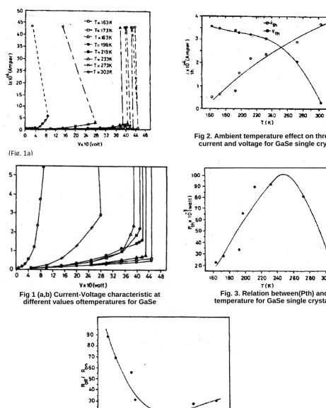
Fig. 1-a represents the DC current-voltage characteristics of GaSe in temperature range extending from (163 to 303K), when the current flows parallel to layers (perpendicular to C-axis). It is seen that the l-V characteristics are strongly influence by surrounding temperature. With increase in temperature, the l-V characteristic as whole is shifted toward the lower potentials. The conduction state can be kept at a certain holding current (ih) and holding voltage (Vh). The
holding voltage (Vh,) increases with temperature,
while the holding current (ih) is independent on temperature and has the temperature, while the
holding current (ih) is independent of
temperature and has the same value at the whole temperature range of investigation. It is clear from the curves in fig. (1-a) that at low DC voltage, the l-V characteristic is nearly close to linear curve.
With increase in applied voltage, the dependence of current on voltage gradually becomes non-linear. Fig.(1-b) illustrates the lower part (0-6x10 -4
Amper) of fig. (1-a). Increasing the applied voltage to a certain value (threshold voltage Vth), the crystal goes into a negative state (ON State) in which the series resistor limits the voltage applied to prevent destruction of the crystal. When the voltage decreased, the ON state may be maintained and the material retain back to its original state in few seconds. This effect is
termed switching with memory. Switching
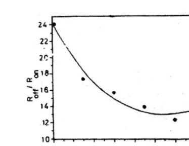
behavior takes place at electric field value (0.25x10³ V/cm) at room temperature. Near switching delicate control of the applied voltage is required since an increase of (0.1-volt) is sufficient to move the device from a stationary condition to a switching condition. The switching process takes place with both polarities on crystal and the current- voltage characteristics of GaSe are symmetric relative to polarity of the applied field. The variation of the switching parameters (ith,vth) with temperature for GaSe single crystal are shown in fig.(2). The threshold voltage (vth) is observed to drop rapidly with increasing temperature while the threshold current (ith)
increase monotonically with increasing
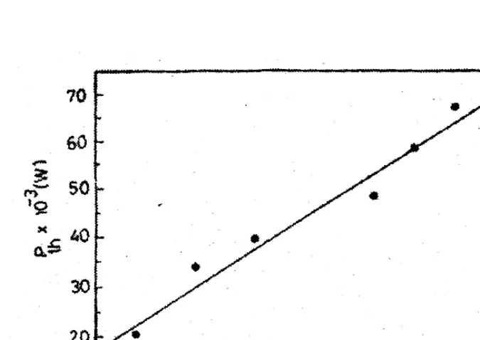
temperature. Fig. (3) Shows the temperature dependence of the power at threshold (Pth) for GaSe. It is found that the threshold power increases with increasing temperature reaches a maximum value (98x10-3 watt) corresponding to (250K) and after that the threshold power decreases exponentially with increasing tem-perature reaches a minimum value at (303K). Fig.(4) shows the dependence of resistance ratio
(Roff/NoN) for this compound on temperature. It is
clear that this ratio increase with the decrease of temperature. The resistance ratio varies from (18.743) to (88.507) in the range of temperature of investigation.
110 A.A. Al-Ghamdi, eta/., MaterialSci. Res. India 02(2) 107-114 (2004)
(Fig. 1a)
Fig 1 (a,b) Current-Voltage characteristic at different values oftemperatures for GaSe
single crystal.
Fig. 3. Relation between(Pth) and temperature for GaSe single crystal.
Fig. 4.Temperature dependence of ROH/R«I for GaSe single crystal.
A A Al-Ghamdi, et a/.. Material Sci. Res. India 02(2) 107-114 (2004) 111
Fig. 9. The effect of GaSe sample thickness on the l-V charactreristics. Fig. 5. The effect of light intensity on
l-V characterstics for GaSe single crystal.
Fig. 8. Light intensity dependence of
(Roff/Ron) for GaSe single crystal.
Fig. 6. Dependance of ith and Vth on light intensity for GaSe single crystal.
Fig. 7. The effect of light intensity on the threshold power (Pth) for GaSe
6
112 A.A. Al-Ghamdi, eta/.. MaterialSci. Res. India 0 2 ( 2 ) 107-114 (2004)
Fig. 10. Variation of ith and vth with GaSe sample thickness.
A.A. Al-Ghamdi, et al.. Material Sci. Res. India 02(2) 107-114 (2004) 113
Fig. 12. THe ratio between OFF and ON state resistivities.
ture under illumination with light of different intensities in the range (Zero,300,600,900, 1200,1500 Lux). It is evident from the figure that the l-V characteristics as whole are shifted toward lower potentials with increases in the intensity of the incident light. The characteristic behavior can be described as follows:
a- Values of high resistance state decrease by increasing light intensity.
b- The field necessary for switching to be performed is reached early on increasing the light intensity dose.
c- Near switching delicate control of the applied voltage is required. The holding voltage (Vh)
decreases as the intensity of illumination increase, while the holding current (ih) does not vary with the intensity of illumination.
The threshold current (ith) increase with
increasing of light intensity while the threshold voltage decrease rapidly with increasing intensity as shown in fig. 6. The relation between threshold power (Pth)with
light intensity is presented graphically in fig. 7. As we notice, (Pth) decreases linearly with increasing
the incident light intensity. This may be due to the photogeneration processes that take place under illumination of sample and lead to low power for switching as the intensity dose increases. The dependence of the resistance ratio (R0ff/RoN> on
illumination intensity is shown in fig. 8. This ratio decreases as the light intensity increases. The ratio decreases as the light intensity increases. The ratio (Rott/RoN) varies from 12.31 to 23.7 in range of light intensity.
114 A. A. Al-Ghamdi, eta/.. MaterialSci. Res. India 02(2) 107-114 (2004)
the dashed line which represent the variation from OFF to ON state decreases with thickness. This result indicates that the switching can be easily controlled with sample thickness. It is also observed from the curve that the holding voltage (vh) increases with the decrease of sample thickness and its value lies between (21-50) volt whereas the holding current (ith) is independent
on the sample thickness and has the value (4.3mA). It is clear from the curves in Fig. 10 that the threshold voltage decreases rapidly with increasing the sample thickness while the
threshold current increase exponentially with sample thickness. The variation of the threshold power (Pth) with sample thickness plotted in Fig.
11. It is seen that the threshold power increases linearly with increasing thickness, i.e. the power required for switching decrease as the thickness of the sample decreases. The ratio between OFF and ON state resistivities decreases with thickness and reach a very low value at higher thickness as shown in fig. (12). The resistance ratio varies from 14.87 to 108.6 in the range of sample thickness under test.
REFRENCES
1. S. M. Atakishev and G. A. Akhundov,
Phys. Status Solid, 32K33 (1969). 2. C. De Blasi, G. Micocci, A. Rizzo, and
A. Tpore, Phys. Stat. Sol., (a)74, 291 (1982).
3. B.G. Tagiev, G.M. Niftiev, and F. Sn. Aidaev, Phys. Stat. Sol., (a)89, 639 (1985).
4. A. Segure, F. Pomer, A. Cantarero, W. Kraause, and A. Chevy, Phys. Rev,
B, 29, 5708 (1984).
5. A. Sequre, B. Mari, J. Martinez-pastor, A.Chevy, Phys. Rev., B, 43, 4953 (1991). 6. J. Riera, A. Sequre, and A. Chevy, Phys.
Stat. Sol., (a),136, K47, (1993).
7. J. Camassel, P. Marel, H. Mathie and A. Chevy, Phys.Rev., B, 17, 4718 (1978). 8. V.S. Vneprouskii, A.I. Furtichev, VJ. Klonov,
E.V. Nazvanova , D.K. Okorov and V.U. Vanadish, Phys. Status. Solidi, a, 145.
341 (1988).
9. E. Bringer, A. Bourdon, N. Piccioli and A.
Chevy, Phys. Review, B, 49,16971
(1994).
10. A.G. Kyazym-Zade, R. N. Mekhtieve, and A.A. Akhmedove, Sov. Phys. Sem-icond 25, 840 (1992)..
11. C.E.M. Campos, J.C. De Lima, T. A. Grandi, K. D. Machado, P. S. Pizani,
Solid State Commun., 126. 611 (2003).
12. Levy, Crystallography and Crystal
Chemistry of Materials with Layered Structures (Reidel, Dordrecht, (1976). 13. Vito Capozzi, Phys. Rev., V., 28 N8,
4620-4627 (1983).
14. A. T. Nagat, S. A. Hussein, and Y. H. Gameel, Indian Jour, of Pure andAppl. Phys., 28, 586 (1990).
15. S. A. Hussein, A. T. Nagat, and Y. H. Gameel, EgyptionJ. Sol., 10,45 (1988).
16. A. O. Kodalbas and G. M. Mamedov,
Material Science and Engg. B 110, 52 (2004).
17. W.D. Buckly and S.H. Holmberg., Solid State Electronics, 18, 127 (1975). 18. H. Martinez and J. T. Piqueras, Solid
State Electronics, 27, 937 (1984). .19 S.A. Hussein, Crystal Res Techno/, 24,
467(1989).
20. A.T. Nagat, S.A. Hussein, Y.H. Gameel and G.A. Gamal, Crystal Res Techno/.,
25, 1195 (1990).