LOW POWER AND LOW JITTER
PHASE FREQUENCY DETECTOR FOR
PHASE LOCK LOOP
KRUTI P. THAKORE
Electronics and communication department, L D R P institute of technology, Gandhinagar, India
HARIKRISHNA C. PARMAR
ECC Department, C K Pithawalla collage of Engg. & technology, Surat , Gujarat
Dr.N.M. DEVASHRAYEE
PG Co-ordinator, VLSI Design, EC Branch Nirma University, Ahmedebad, India
Abstract:
This paper presents three types of phase frequency detectors – traditional PFD, modified PFD and high speed PFD. With the comparison of Low power and low jitter phase frequency detector the high speed phase frequency detector is the best candidate for this. High speed phase frequency detector is operated at 1GHz input frequency with 1.8v power supply, power consumption of .39nwatt and jitter is only 2ps. The design is simulated with .35µm CMOS technology.
Keywords:, Low Power, Low Jitter PLL
1. Introduction
In recent years, the design of low power and low jitter PLL for the different application has become one of the greatest challenges in high-performance very large scale integration (VLSI) design. As a consequence, many techniques have been introduced to minimize the power consumption and reduction in jitter of new VLSI circuits.
Integrated phase-locked loops (PLL's) play the versatile roles in the applications of clock generator, time synchronization and clock multiplication. A typical Phase Lock Loop architecture is depicted [2]. It consists of a phase frequency detector (PFD), a charge pump, a loop filter, a voltage-controlled oscillator (VCO) and a frequency divider. [6] [7] Each building block contributes to the PLL output timing jitter, so improved circuit of phase frequency detector is proposed in this paper for low jitter and low power.
The methodology of low-jitter PLL design has been developed in recent years. The jitter of PLL primarily is contributed from the reference clock, phase frequency detector, supply noise, substrate noise, charge pump circuit and VCO internal noise. [1] [8]
The tradition Phase Frequency Detector having two D-flip flop and a AND Gate in the reset path. [3] As this traditional PFD is designed in CMOS .35µm technology the out put of D flip flop is inverted output so, in place of AND Gate in the design NOR Gate is used to get the proper output. Implementation of D Flip-flop and NOR gate is as shown in the figure. Input to the PFD is form the reference clock which is the system clock or the processor clock. The range of the clock is normally mega hertz .The tradition PFD in this paper is operated at 50 MHz frequency.
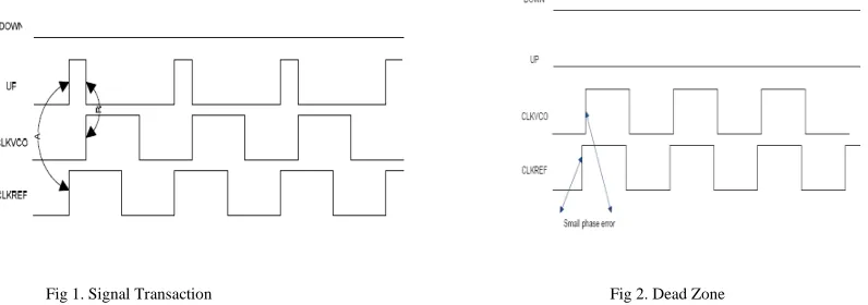
Fig 1. Signal Transaction Fig 2. Dead Zone
From the figure 1, signal transaction, when clkref signal is going high it will charge the upper D flip flop and resulting in changing the UP signal to high. Same for clkvco, when clkvco signal is going high it will result the DWN signal changing to high. This will result both the inputs of AND gate high and make the reset signal high to make both outputs low. It is known as the lock condition for the PFD when both the outputs of PFD – UP signal and DWN signal are low. When clkref is leading it will result the UP signal high as shown in figure 1, same for clkvco result the DWN signal high. The width of the UP signal or DWN signal is the measure of error. With the use of this error the control voltage is generated and then that will correct out the frequency difference between input CLK and the clock coming from the VCO from feedback path of the PFD.
Figure 3. Implementation of Traditional PFD Figure 4. Traditional PFD at 50 MHz
In this case the sensitivity of the means the smallest difference the PFD can detect and produce at the output UP or DOWN signal. This lead to the conclusion that the higher the sensitivity the better the PFD.
One of the disadvantages that the tradition PFD suffers is dead-zone. Dead-zone is a small difference in the phase of the inputs that a PFD will not be able to detect. Due to dead zone jitter will produce at the output.
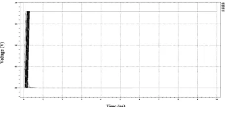
Figure 5. Dead Zone of Traditional PFD
For actual result we can see figure 5. The implementation is using CMOS 0.35μm technology with 1.8v as a supply voltage. The input CLK frequency is 50 MHz. The power consumption of this PFD is 45.5 μW and the NOR gate needs around 80 Pico seconds to charge up and be able to reset both flip-flops so, the size of the dead zone is 70 Pico second.
The disadvantage of this traditional PFD is that the reset path with NOR gate which increases the dead zone and it will result in jitter. So, modification has been done with this design to reduce the power consumption and the size of the dead zone.
2.2. Modified PFD with Modified D flip flop
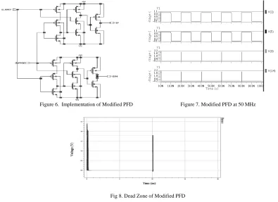
Fig 8. Dead Zone of Modified PFD
With this new modified circuit of PFD the power consumption is reduced and the dead zone is also reduced. With the figure 8 the reduced dead zone is observed. In this type of modified PFD 35ps of dead zone is achieved. So, the output jitter is reduced with this circuit of modified PFD.
Still the dead zone is high so, the new technique is introduced which is known as high speed PFD with the total elimination of the reset path. With the elimination of reset path the reset time is reduced. By this technique the jitter is reduced. The high speed phase frequency detector is introducing in next section.
2.3.A High Speed PFD
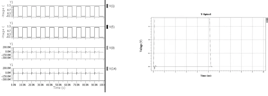
Still improvement is possible with high speed PFD which is another way to reduce the power consumption and the jitter. In this circuit two invertors and NAND gates are added. The implementation of the high speed PFD with CMOS .35µm technology is as shown in the figure 9. In this PFD high speed is also achieved by detection of both the rising and falling edges of input signals.
Figure 9. Implementation of High Speed PFD Figure 10. High Speed PFD at 50 MHz (Lock Condition)
Figure 11. High Speed PFD at 50 MHz (CKLOUT Leading) Figure 12. High Speed PFD at 50 MHz (CKLREF Leading)
The high speed phase frequency detector is simulated at 50MHz input frequency with power consumption of .87nw. This is the smallest power consumption achieved compare to other two types of phase frequency detectors.
Figure 14. High Speed PFD at 100MHz Figure 15. Dead Zone of High Speed PFD (at 100MHz)
As shown in figure 14 the high speed PFD is at input frequency 100 MHz. This figure shows the lock condition of the high speed PFD. Power consumption of high speed phase frequency detector is .48nwatt @ 100MHz frequency. From the figure 15 the dead zone can be observed. The dead zone of the high speed PFD at 100MHz is 6ps.
Figure 16. High Speed PFD at 1GHz Figure 17. Dead Zone of High Speed PFD (at 1GHz)
Here figure 16 shows the simulated output of high speed phase frequency detector at 1GHz input frequency lock condition. Power consumption of high speed PFD at 1GHz input frequency is .39nwatt. Form the figure 17 the dead zone of this PFD can be observed. Dead zone of high speed PFD at 1GHz is only 2ps. This is the approximate zero jitter for the phase lock loop contributed by high speed phase frequency detector.
3. Experimental results with comparison tables
TABLE I. Comparison of three types of PFD for jitter and power at 50MHz
PFD JITTER POWER Traditional PFD 70ps 45.5μW
Modified PFD 35ps 2.06nW
High Speed PFD 14ps .87nw
TABLE II .Comparison of jitter and power for high speed PFD with different frequency
FREQUENCY JITTER POWER 50MHz 14ps .87nwatt
100MHz 6ps .48nwatt
Conclusion
This paper has presented three types of phase frequency detectors – traditional, modified and high speed. With comparison of these three PFD for low jitter and power the high speed phase frequency detector is the best candidate for this. At 1GHz input frequency with 1.8v power supply the power consumption is only .39nwatt and jitter is only 2ps. The design is simulated with .35µm CMOS technology.
References
[1] Wen-Chi Wu,C,h ih-Chien Huung, Chih-Hsiung Chang'. and Nui-Heng Tseng:”Low power CMOS PLL for clock generator.”IEEE International synopsis on circuits and systems,2003,vol-1,PP.I-633-I-636
[2] Xintian Shi, Kilian Imfeld, Steve Tanner, Michael Ansorge and Pierre-André Farine:”A Low-Jitter and Low-Power CMOS PLL for Clock Multiplication” IEEE ,solid state circuits,2006,pp. 174-177
[3] Mhd Zaher Al Sabbagh, B.S.: 0.18μm Phase / Frequency Detector and Charge Pump Design for Digital Video Broadcasting for Handheld’s Phase-Locked-Loop Systems. Thysis,2007
[4] Kyung Ki Kim, Yong-Bin Kim :” A 32nm and 0.9V CMOS Phase-Locked Loop with Leakage Current and Power Supply Noise Compensation”
[5] Ms. Ujwala A. Belorkar and Dr. S.A.Ladhake :” Design of low power phase locked loop ( PLL) using 45nm VLSI Technology.” International journal of VLSI design & Communication Systems ( VLSICS ), Vol.1, No.2, June 2010
[6] Abishek Mann, Amit Karalkar, Lili He, and Morris Jones :” The Design of A Low-Power Low-Noise Phase Lock Loop” IEEE international Synopsys ,qulity electronic design, 2010 ,pp.,528-531
[7] Yingmei, Chen†; Zhigong, Wang; Li, Zhang “Design of a Dual Mode Clock Generator Based on a PLL Structure ”IEEE power and energy engineering conference (APPEEC) ,15 April 2010 Asia – pacific ,pp.,1 - 3
[8] Vincent von Kaenel, Daniel Aebischer, Christian Piguet, Evert Dijkstra:” A 320MHz, 1.5mW at 1.35V CMOS PLL for Microprocessor Clock Generation “IEEE journalof solidstate circuits,1996,pp., 1715-1722