Analysis and Design for a High Power Density
Three-Phase AC Converter Using SiC Devices
Rixin Lai
Dissertation submitted to the faculty of the Virginia Polytechnic
Institute and State University in partial fulfillment of the
requirements for the degree of
Doctor of Philosophy
In
Electrical Engineering
Committee:
Dr. Fred Wang (Chair)
Dr. Dushan Boroyevich
Dr. Rolando Burgos
Dr. Yilu Liu
Dr. Tao Lin
December 10, 2008 Blacksburg, VirginiaKeywords: high power density, SiC devices, passive component
minimization, topology evaluation, high performance control development,
Three-Phase AC Converter Using SiC Devices
Rixin Lai
Abstract
The development of a high-power-density three-phase ac converter has been a hot topic in power electronics due to the increasing need in applications like electric vehicles, aircraft and aerospace, where light weight and/or a low volume is usually a must. There are many challenges due to the complicated relationships in a three-phase power converter system. In addition, with the emerging SiC device technology, the operating frequency of the converter can be potentially pushed to tens of kHz to hundreds of kHz at high-voltages and high-power conditions. The extended frequency range brings opportunities to further improve the power density of the converter. The technologies based on existing devices need to be revisited.
In this dissertation, a systematic methodology to analyze and design a high-power-density three-phase ac converter is developed. All the key factors of the converter design are investigated with the goal of high power density. The dissertation is divided into five sections. Firstly, the criteria for passive filter selection are derived, and the relationship between the switching frequency and the size of the EMI filter is investigated. A functional integration concept is proposed together with the physical design approach. Secondly, a topology evaluation method is presented, which provides insight into the
Four topologies are then compared with the proposed approach, culminating with a preferred topology under the given conditions. Thirdly, a novel average model is developed for the selected topology, and is used for devising a carrier-based control approach with simple calculations and good regulation performance. Fourthly, the converter failure mode operation and corresponding protection approaches are discussed and developed. Finally, a 10 kW three-phase ac/ac converter is built with the SiC devices. All the key concepts and ideas developed in this work are implemented in this hardware system and then verified by the experimental results.
I owe an enormous debt of gratitude to my advisor, Dr. Fred Wang, for his patience, support, guidance and belief during my study as well as my daily life. He taught me something beyond just techniques for solving problems and led me to a new world full of challenges and opportunities. His profound knowledge, gentle personality and rigorous attitude toward research will benefit my career as well as my whole personal life.
I would like to express my appreciation to my committee member, Dr. Dushan Boroyevich, who has very creative thinking and also a sense of humor, for his instruction and many vivid ideas. I would like to thank Dr. Rolando Burgos, who always has infectious enthusiasm on work and daily life, for his help and time at many aspects. I would also like to thank my other committee members Dr. Yilu Liu and Dr. Tao Lin for always helping and encouraging me during my time as a graduate student.
I would also like to thank all my colleagues in CPES for their help, mentorship, and friendship. I cherish the wonderful time that we worked together. Although this is not a complete list, I must mention some of those who made valuable input to my work. They are Dr. Shuo Wang, Dr. Ming Xu, Dr. Yunqing Pei, Dr. Wei Shen, Dr. Qian Liu, Dr. Hongfang Wang, Honggang Sheng, Jerry Francis, Carson Baisden, Tim Thacker, Ball Arthur, Arnedo Luis, Reusch David, Doug Sterk, Dianbo Fu, Chuanyun Wang, Jing Xu, Michele Lim, Yan Liang, Sebastian Rosado, Yoann Maillet, Yi Sun, Jian Li, Pengju Kong, Ruxi Wang, Dong Dong, Zheng Chen, Qian Li, Xiao Cao, Tong Liu, Daocheng Huang, Ying Lu, Jing Xue, and so many others. In particular, I would like to thank Puqi Ning, Di Zhang, Dong Jiang and Zhiyu Shen for their help and time on this project.
Martin, Teresa Shaw, Trish Rose, Elizabeth Tranter, Linda Gallagher and Dan Huff, who always smiled at me and helped me to get things done smoothly.
I offer my deepest gratitude to my girlfriend, Yan Jiang, my aunt, Jufen Xie, my brother, and my mom and dad, for their love, support and confidence in me.
Chapter 1 Introduction... 1
1.1 Background... 1
1.2 State-of-the-art Research ... 8
1.3 Research Challenges and Objectives ... 13
1.4 Dissertation Organization ... 15
Chapter 2 Passive Filter Minimization ... 17
2.1 Introduction on Filter Design... 17
2.2 Passive Parameters Selection and Minimization ... 20
2.2.1 Switching Frequency Selection and EMI Filter Design ... 20
2.2.2 Boost Inductor and DC-Link Capacitor Design... 30
2.2.3 Simulation Verification... 34
2.3 Summary ... 38
Chapter 3 Topology Evaluation... 39
3.1 Introduction... 39
3.2 Evaluation Approach ... 42
3.3 Topology Comparison ... 52
3.4 Summary ... 69
Chapter 4 Modeling and Control for Non-Regenerative Three-Level Boost Rectifier. 71 4.1 Introduction... 71
4.2 Average Model Derivation ... 74
4.3 Proposed Controller ... 79
4.6 Summary ... 94
Chapter 5 Failure Mode Analysis and Protection... 95
5.1 Introduction... 95
5.2 Neutral Switch Shorted Failure of Vienna-Type Rectifier ... 98
5.2.1 Fault Mechanism Analysis... 98
5.2.2 Over Voltage Protection ... 100
5.2.3 Experimental Verification... 110
5.3 Shoot-Through Failure and Protection... 112
5.3.1 Proposed Protection Approach ... 112
5.3.2 Gate Driver Circuit Design ... 115
5.3.3 Experiment Results ... 117
5.4 Summary ... 119
Chapter 6 Hardware Development and Experiments ... 121
6.1 System Configuration and Interface ... 121
6.2 Hardware Design and Construction... 123
6.2.1 Digital Controller ... 123
6.2.2 DC Bus Board... 124
6.2.3 Input Filter ... 127
6.2.4 Phase Leg Module and Gate Drive ... 129
6.2.5 SiC JFET Characterization ... 134
6.3 System Assembly and Test ... 135
6.3.3 Experimental Results ... 138
6.4 System Efficiency ... 144
6.5 Weight Discussion for the Hardware System ... 146
6.6 Summary ... 148
Chapter 7 Conclusions and Future Work ... 150
7.1 Conclusions... 150
7.2 Future Work... 152
Figure 1-1 Power density roadmap for power electronics converters [7]... 2
Figure 1-2 Comparison of SiC and Si based devices [9] ... 3
Figure 1-3 Switching loss comparison between Si-pin diode and SiC Schottky diode [9] 4 Figure 1-4 Shipboard motor drive [11]... 5
Figure 1-5 Weight distribution of shipboard converter system [11]... 5
Figure 1-6 Approaches to achieve high power density... 6
Figure 2-1 Diagram for back-to-back VSC ... 18
Figure 2-2 Spectrum analysis for SVM ... 22
Figure 2-3 Spectrum analysis for DPWM ... 23
Figure 2-4 Differential mode noise... 25
Figure 2-5 Common mode noise... 25
Figure 2-6 Corner frequency vs. switching frequency... 26
Figure 2-7 Two-stage EMI filter... 26
Figure 2-8 DM noise spectrum around the first order switching frequency... 29
Figure 2-9 Required inductance for power quality standard and EMI standard... 29
Figure 2-10 Cascaded subsystem diagram... 32
Figure 2-11 Impedance bode plot ... 32
Figure 2-12 Failure mode comparison for 10uF and 100uF DC link capacitance... 34
Figure 2-13 Circuit diagram for Vienna rectifier... 34
Figure 2-14 Simulation results for load step change (The top traces are the capacitor voltages, the bottom traces are the source input current.)... 35
bottom traces are the capacitor voltages.)... 36
Figure 2-16 Harmonic current spectrum... 37
Figure 2-17 EMI spectrum... 37
Figure 3-1 Key components for an ac-ac converter... 42
Figure 3-2 Topology evaluation procedure... 43
Figure 3-3 Device thermal structure illustration... 46
Figure 3-4 Thermal equivalent model... 46
Figure 3-5 CL-CL filter for CSC ... 49
Figure 3-6 Design variables for the EE core... 51
Figure 3-7 Design variables for the toroid core ... 51
Figure 3-8 (a) Back-to-back VSC, (b) Non-generative three-level boost rectifier plus voltage source inverter, (c) Back-to-back CSC and (d) 12-switch matrix converter... 53
Figure 3-9 Simulation results for BTB-VSC: (a) ac-line currents; (b) PWM line-to-line voltage... 54
Figure 3-10 Vector synthesis in sector I of space vector diagram... 55
Figure 3-11 Pulse pattern for the top switches in the first 30° ... 55
Figure 3-12 Simulation results for NTR-VSI: (a) ac-line currents; (b) PWM line-to-line voltage... 58
Figure 3-13 Spectrum of the PWM voltage for NTR-VSI ... 59
Figure 3-14 Simulation results for BTB-CSC: (a) ac-line source currents; (b) rectifier input current ... 60
PWM line current... 63
Figure 3-17 Spectrum of the PWM current for matrix converter ... 63
Figure 3-18 Weight comparison of four topologies under consideration... 65
Figure 3-19 Formulation of the converter optimization ... 68
Figure 4-1 Rectifier topology... 74
Figure 4-2 State space average model ... 78
Figure 4-3 Neutral point voltage control loop ... 78
Figure 4-4 Time domain waveform of d0’ (M=1, ω0=400 Hz)... 79
Figure 4-5 Spectrum of d0’ (M=1, ω0=400 Hz) ... 80
Figure 4-6 Control scheme diagram ... 80
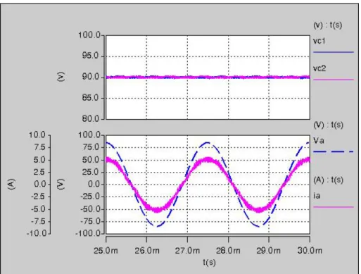
Figure 4-7 Steady state simulation results (The top traces are the voltages across the two dc-link capacitors respectively. The bottom two traces are the input voltage and the line current of phase A.)... 83
Figure 4-8 Simulation results of load step up transient (The top traces are the dc link voltages. The bottom traces are the input phase currents.) ... 83
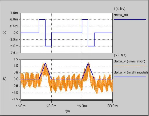
Figure 4-9 Voltage unbalance behavior under pulsating ∆d0 (The top trace is the waveform of ∆d0. The bottom traces show the dc-link voltage unbalance corresponding to the given ∆d0. The light color line is the simulation result and the dark color line is the calculation result from the proposed model.) ... 84
(Traces from top to bottom: dc-link voltages, rectifier pole to pole voltage VAB, and
input current of phase A.) ... 86
Figure 4-12 Steady state results with the carrier-based control scheme... 86
Figure 4-13 Dc-link voltage unbalance with the carrier-based control scheme ... 87
Figure 4-14 Steady state results with the space vector based control approach ... 87
Figure 4-15 Dc-link voltage unbalance with the space vector based control approach.... 88
Figure 4-16 Measured duty cycle components of the proposed carrier-based control scheme (The top traces are the duty cycles for three phases. The bottom trace is the zero sequence component.)... 88
Figure 4-17 Measured duty cycle components of the space vector control scheme (The top traces are the duty cycles for three phases. The bottom trace is the zero sequence component.) ... 89
Figure 4-18 Space vector diagram in 60º... 90
Figure 5-1 Circuit diagram of the non-regenerative three-level boost rectifier... 98
Figure 5-2 Circuit structure when Qa is shorted ... 99
Figure 5-3 Simulation results during the Qa short: the top traces are capacitor voltages, the bottom traces are input currents ... 99
Figure 5-4 (a) Diagram for the voltage clamping protection circuit, (b) simplified circuit for peak voltage approximation ... 101
Figure 5-5 Simulation results for resistor clamping ... 102
(d) mode 3 ... 105
Figure 5-8 Impact of L and k on the peak fault current ... 108
Figure 5-9 Impact of L and k on the dc-link power dissipation ... 108
Figure 5-10 Circuit diagram for current breaking approach... 109
Figure 5-11 Simulation results for current breaking approach ... 110
Figure 5-12 Experimental waveform neutral switch shorted failure without protection 111 Figure 5-13 Experimental waveform neutral switch shorted failure with current breaking protection approach... 112
Figure 5-14 Proposed protection circuit ... 113
Figure 5-15 Modes of operation ... 114
Figure 5-16 Gate driver circuit for protection... 116
Figure 5-17 Experimental setup for shoot-through protection ... 117
Figure 5-18 Experimental results: Traces from top to bottom: gate to source voltage of IGBT (Vge), drain to source voltage of MOSFET (Vds), drain current of MOSFET (Id) and collector to emitter voltage of IGBT (Vce)... 118
Figure 6-1 Hardware system circuit diagram... 121
Figure 6-2 Hardware system interface... 123
Figure 6-3 Structure of the controller ... 124
Figure 6-4 Diagram of the dc bus board ... 125
Figure 6-5 Circuit diagram of the dc bus including protection... 126
Figure 6-6 Voltage sensing circuit... 126
Figure 6-9 Physical structure of the input filter ... 128
Figure 6-10 Rectifier phase leg... 129
Figure 6-11 Inverter phase leg ... 129
Figure 6-12 Gate driver circuit ... 130
Figure 6-13 Phase leg modules ... 131
Figure 6-14 Test circuit for the inverter phase leg... 131
Figure 6-15 Waveforms of top switch turn on... 132
Figure 6-16 Waveforms of top switch turn on with additional 1.5 nF capacitor... 133
Figure 6-17 Waveforms of top switch turn off with additional 1.5 nF capacitor ... 133
Figure 6-18 RDS,on versus temperature ... 134
Figure 6-19 System assembling... 135
Figure 6-20 Controller structure ... 136
Figure 6-21 Start-up sequence ... 137
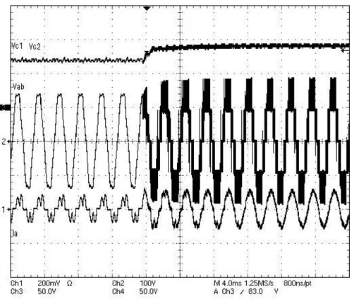
Figure 6-22 System start-up transient waveforms ... 138
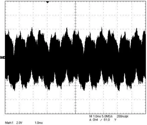
Figure 6-23 Steady state waveforms at full power ... 139
Figure 6-24 Input current spectrum analysis ... 140
Figure 6-25 EMI measurement results... 141
Figure 6-26 Motor test setup... 142
Figure 6-27 Measurement results for the rectifier ... 143
Figure 6-28 Measurement results for the inverter... 143
Table 2-1 Double Fourier Integral Limits for SVM (Phase A) ... 21
Table 2-2 Outer and Inner Double Fourier Integral Limits for DPWM (Phase A) ... 22
Table 2-3 Harmonic Current Limits ... 27
Table 2-4 Operation Conditions and Design Results... 35
Table 3-1 System Specifications... 54
Table 3-2 Design Results for BTB-VSC ... 65
Table 3-3 Design Results for NTR-VSI... 66
Table 3-4 Design Results for BTB-CSC... 67
Table 3-5 Design Results for 12-Switch Matrix Converter ... 67
Table 4-1 Parameters Used in Simulation ... 82
Table 5-1 Parameters Used in Experiment ... 111
Table 6-1 Physical Parameters for the CM Choke... 128
Table 6-2 Switching energy under different conditions (@ 25°C)... 134
Table 6-3 Circuit Parameters for the experiment... 139
Table 6-4 Conditions for the Motor Test ... 142
Table 6-5 Efficiency Measurement... 144
Table 6-6 Loss Calculation @ Estimated Junction Temperature of 56.5C ... 145
Chapter 1
Introduction
This chapter starts with an introduction to the background of high-power-density three-phase ac converters. The state-of-the-art research activities in the corresponding area are reviewed, which helps to identify this work and its originality. The challenges and the scope of high-density design are then presented, followed by an explanation of the structure of the dissertation.
1.1 Background
High power density is one of the key topics for the continual development of power electronics converters [1]. Power converters are designed not only to meet the input and output requirements, but also to achieve a low volume or a light weight in many specific applications. The demand for reduced converter volume is usually driven by the requirements in information technology or hybrid vehicles due to the limited space as well as the progress of the integrated circuit technology [2]-[4]. Additionally, a low converter weight is particularly important for applications in aircraft and avionics, where the weight has a dramatic impact on the cost and feasibility of the operation and maintenance [5], [6].
There has been a large increase in the power density of the power electronics converters over the last few decades, which covers a wide range of applications and converter types. This trend is shown in Figure 1-1 [7]. The increase of power density is mainly achieved by increasing the switching frequency, enabled by faster and lower loss devices. In the early stages of power electronics converters, the power density was
relatively low due to the limited speed of the available switching devices (SCR and GTO), which usually operated at less than hundreds of Hz. Since the 1990’s, the power density of the converter has improved greatly with the development of power high-switching-frequency devices, like IGBTs and MOSFETs. Figure 1-2 indicates that further improvement is expected in the near future with the implementation of SiC devices.
Figure 1-1 Power density roadmap for power electronics converters [7]
The SiC wide band-gap power semiconductor switches and diodes can potentially bring significant improvement to the design of the converter system. The SiC field effect transistor (FET) is expected to out-perform the Si IGBT and Si MOSFET in high voltage ranges due to their low on-resistance and very fast switching characteristics [8]. Figure 1-2 shows the static behavior of the most popular switches as well as the SiC Cascode device [9]. For comparison, the devices are chosen with a breakdown capability of 1000 V and a 1 cm2 die size. As can be seen from Figure 1-2, the SiC switching device shows much better performance in terms of forward voltage drop. High-voltage SiC Schottky diodes also show very promising static and dynamic characteristics [10]. Figure 1-3
shows the switching loss of a SiC Schottky diode compared to a Si pin diode [9]. In addition to the electrical characteristics, these devices have a higher maximum operation junction temperature, which can potentially lead to reduced cooling effort. The features of the SiC devices provide the possibility of a high switching frequency with low loss, and therefore the flexibility to further improve the converter system design over a very wide frequency range. Technology evaluation and converter design approaches based on existing devices and materials should be revisited and modified in order to fully utilize the SiC devices and further improve the power density. For this reason, SiC devices are selected in this work while studying the high-density power converters.
Figure 1-3 Switching loss comparison between Si-pin diode and SiC Schottky diode [9]
A power electronics converter usually consists of the following elements [1]:
• Passive filter components (input/output filter, dc-link filter)
• Cooling system
• Power semiconductors
• Control circuit and auxiliaries
• Interconnection and housing
The size and weight distribution of these elements is highly dependent on the converter structure and the system requirements. There are thousands types of topologies which vary with the application. Different types of topologies may require various approaches for high-density analysis and design. This work focuses on three-phase ac converters, since they are currently widely used in the electric transportation system
(electric vehicle/ship/aircraft) to drive variable speed motors, where high-power-density is usually necessary [2], [6], [11].
Figure 1-4 Shipboard motor drive [11]
Figure 1-5 Weight distribution of shipboard converter system [11]
Figure 1-4 shows the diagram for a shipboard motor drive as an example of a three-phase ac converter [11]. The size and weight of the converter are heavily influenced by the interface requirements that are imposed on the system. Those interface requirements
include not only electric compatibility, such as power quality standard and EMI standards, but also mechanical concerns, such as shock and vibration. Reference [11] carries out example designs for two different standards, and the components weights of the whole system are shown in Figure 1-5 [11], indicating that for both passive filter designs, the cooling system and the housing are the key contributors to the weight. The housing usually is related to the system profile. Its size and weight will be reduced if the overall size is reduced. Therefore this work did not put special effort on reducing the size and weight of the housing.
Reduce Passives
•High switching frequency
•Circuit & filter topology
•Components & materials
•Integration
• Topology for reduced noises, losses, filter needs
• SiC devices for low loss, high frequency, & high temperature
• Passive materials & components
• Design limit and optimization
High-density Converter High-density Converter
Reduce Heatsink
•Low loss
•High junction temperature
•Cooling technology
Figure 1-6 Approaches to achieve high power density
There are two ways to reduce the size of the converter by changing the electrical components. One is to reduce the passive filter; the other is to reduce the heatsink, as shown in Figure 1-6. In order to achieve the first objective, several approaches may be appropriate: raise the switching frequency, improve the circuit and filter topology, use new components and materials, and use advanced integration technology. Using a higher
switching frequency is a common practice for reducing the passive components. As mentioned above, the feasible switching frequency range has been greatly extended by the advanced SiC device technology, which will lead to new opportunities for higher-density design. Different circuit topologies will have different noise levels, loss performance, and energy storage requirements; therefore their choice will significantly impact the size of the passive components and the heatsink. Components and materials selection as well as the integration approach are clearly important aspects to reducing the component size. For the heatsink reduction, the effort is on reducing the loss and increasing the device operating junction temperature while searching for better cooling technologies.
Although the approaches discussed above seem to be common methods in the development of high-power-density power electronics converters, the relationship between the overall system performance and the variables is far from well-understood by average practitioners, especially in the extended frequency range offered by SiC devices. In addition, implementation of SiC devices in high-power three-phase converters remains a challenge due to lack of experience and the normally-on characteristics of the JFET structure. Therefore there is a clear need for a systematic analysis and design approach for high-power-density converters using SiC devices, as well as hardware implementation and verification. The literature review in the next section shows the state-of-the-art status of the research related to the high-power-density three-phase ac converter design and hardware development using SiC devices, which helps to define the challenges and research topics of this work.
1.2 State-of-the-art
Research
The analysis and design for high-density power electronics converters require a wide area in research focus from the classical electrical aspects of topologies, passive filter design, modulation, and control; to other aspects such as the power semiconductors, cooling techniques, magnetic and dielectric materials, interconnection, and packaging approaches. In this work we focus on the research in the classical electrical aspects.
From the system approach standpoint, J. W. Kolar [1] indentified and quantified the technological barriers for high-power-density converters by investigating the volume of the cooling system and the main passive components as functions of the switching frequency. Analysis is carried out for 5 kW rated power while using high-performance air cooling and advanced power semiconductors. The results indicate a volume density limit of 45 kW/dm3 for a three-phase PWM rectifier with the present technology. This paper provided a full vision for the design of high-density power converters in a general sense, but the key correlations between the system requirements and the system parameters are not clearly analyzed and reported. Y. Hayashi [7] [12] proposed a high-density power converter design platform. A power converter is classified by four factors: the power device, the converter circuit, including stray parameters, the passive filter, and control. The relationships among the factors are quantified and stored in the design database, but only the power loss estimation of the converter system was reported in this paper.
The practical approach to achieving high-density design is to investigate the key factors one by one and try to obtain minimum weight design for each of them. Obviously topology is one of the key factors, since it has a dramatic impact on the filter size and loss performance. There has been some previous work on evaluating ac converter topologies
[13]-[16]. Reference [13] compares three ac-dc converter topologies in terms of volume and weight for application in future more-electric aircraft. The loss and the input inductance with the corresponding current’s harmonic performance are analyzed. Reference [14] investigated three-phase converter topologies for integrated motor drives by discussing the hardware requirements and comparing their performance. The evaluation effort focused on the size of the input inductance and the efficiency of the system. Reference [15] calculated and compared the efficiency and loss distribution of the voltage source and current source drive systems. The impact of the switching pattern is considered, and during the comparison the optimized modulation approach is implemented for the current-source converters. Reference [16] evaluates three-level topologies as a replacement for two-level topologies. The input harmonic filter size and the semiconductor loss are carefully studied. The cost and the life time are also estimated in this paper.
In summary, the previous work discussed above focuses on specific aspects of the converter design. The EMI filter, which is one of the main size contributors for active front end rectifier, is usually ignored in the evaluation. Moreover, the previous work concentrated on the evaluation and comparison of some given topologies instead of providing a systematic analysis and selection tool. In-depth understanding of the correlations between system variables and power density is still desired.
Another key aspect for the high-power-density converter is the passive filter component. In terms of function, the passive filter component includes the input harmonic filter, EMI filter, dc-link filter and output filter. The values of the passive components are related to performance requirements, such as EMI and power quality
standards, as well as to the switching frequency and control strategy. Habetler et al. [17] concluded that the voltage source configuration provides the lowest passive component size, and they also studied the effect of the modulation scheme. References [18] and [19] designed the boost inductor based on THD and the switching ripple requirement. Reference [20] proposed a step-by-step design procedure for the LCL filter to limit the switching frequency ripple injection in the range of 2-150 kHz. The boost inductor and the high-frequency stage are designed separately. For the EMI filter, reference [21] provided guidelines for the design of a multistage structure. This study points out that the capacitors and inductors have to be chosen with equal values in order to obtain maximum attenuation with minimum overall capacitance and inductance. Reference [22] designed a differential-mode input filter based on a harmonic analysis of the rectifier input current and a mathematical model of the measurement procedure, including a line impedance stabilization network (LISN) and the test receiver. However [21] and [22] did not investigate the relationship between the switching frequency and the required filter size. P. M. Barbosa [23] studied the DM filter design for a three-phase boost rectifier. The impact of the switching frequency on the EMI filter parameters was studied based on circuit simulation. However, the boost inductor was not considered to be part of the EMI filter in the design stage; therefore overall minimization may not be achieved. For the dc-link filter selection, reference [24] derived the minimum capacitance as defined in terms of power balance. The energy variations for the input rectifier and the motor load over one switching cycle were carefully studied. Reference [19] developed the criteria for dc-link capacitor selection based on the zeros and poles characteristics of the system. References [19] and [24] are highly dependent on the load condition as well as the
control approach, and complicated calculations are required. It is difficult to directly expand these approaches to general cases. For the passive filter, it can be concluded that the relationship between the switching frequency and the passive parameters, especially for the EMI filter, were not well-studied in the aforementioned work. For the input filter, the low-frequency stage and the high-frequency stage are always designed separately, which may lead to oversized selections.
In addition to electrical analysis and design, hardware implementation using SiC devices is also a challenge, due to the normally-on characteristics as well as the special gate driver requirement of JFETs, the fast switching speed, and lack of application experience. There have been increasing research efforts for SiC device hardware development in recent years [25] – [36]. Some of these efforts are focused on dc/dc applications [25] – [28], where the converter topologies are relatively simple and less fault possibility is expected. References [29] and [30] presented a 2 kW three-phase buck rectifier with a 150 kHz switching frequency. The current source topology takes the advantage of the normally-on characteristics. In 2003, reference [31] claimed to have designed the first three-phase inverter using only SiC JFETs. The inverter was tested up to 5700 W/540 Vdc with 4 kHz switching frequency. However the switching speed was limited to 1 kV/μs with a rather large gate resistance. Also in 2003, reference [32] presented a SiC voltage source inverter module, which was tested at 6500 W/250 Vdc with 4 kHz. Arkansas Power Electronics International, Inc. [33] – [35] fabricated a 4 kW high-temperature inverter module with SiC JFETs, which was tested at about 250 °C with 20 kHz switching frequency. Reference [36] presented a 100 kHz, 1.5 kW SiC sparse matrix converter. However SiC cascode devices are utilized instead of SiC JFETs. The Si
MOSFET in the cascade structure provides normally-off characteristics and allowed the use of a conventional high-speed gate driver, but the Si MOSFET also limits the maximum case temperature. Based on the reviews on the previous work for hardware implementation, we can conclude that for the three-phase voltage source inverters using SiC JFETs, only limited power and switching frequencies have been verified by hardware. There is yet to be verification of a three-phase voltage source inverter using SiC JFETs in an ac-ac converter system.
In summary, in terms of electrical design, there has been some research on various aspects for high-power-density converter design, but an in-depth systematic understanding and design tool are still desired. In addition, as the SiC devices advance, the converters operate at higher frequencies and/or have higher power ratings. The corresponding analysis and design have to cater to this need. For the hardware implementation in three-phase converters, the performance of SiC devices was verified with limited operating conditions. Higher power and/or higher switching frequency operation in a full ac/ac system needs to be explored.
We need to emphasize that control design and implementation are also key issues for high-density converters, since the higher switching frequency and smaller passive components will lead to increasing requirements for calculation speed and control performance. Since this depends on the topology, it will be included in the later chapters of this work.
1.3
Research Challenges and Objectives
According to our survey, the state-of-the-art research has investigated various aspects of high-density design for three-phase ac converters. However the system-level understanding and design approach, especially for the extended operation frequency range offered by the SiC devices, is not established. The hardware verification for SiC devices implemented in a full ac/ac system is still desired for higher switching frequencies and/or higher-power operating conditions. Many challenges still exist due to the complicated correlations in the three-phase power converter system and also the new characteristics of the SiC devices.
When developing a new converter for high-density applications, the design must take into account all aspects contributing to the converter size and weight, which requires investigation into the correlation between all major design parameters. There is thus a clear need for a systematic analysis considering the strong interdependence of all design variables and constraints. For example, increasing the switching frequency generally helps to reduce the passive size, but it also increases the converter switching loss and therefore heat sink size. As is shown later in the work, even the relationship between the filter size and switching frequency is not monotonous, due to changing spectrum characteristics and the attenuation requirements of harmonic and EMI standards. Topology is obviously another important aspect for the system design. It impacts the loss, passive filter selection and the control requirement. Determining how to make a fair comparison among different topologies under given conditions is still an issue. The controller is normally not a concern in terms of power density. However, for high-switching-frequency and high-control-bandwidth designs, the controller calculation time
and the regulation performance may become a constraint on the system. Therefore a high-performance control approach is desired to guarantee the design feasibility. Failure mode analysis and the corresponding protection are also significant, especially for applications in the aircraft and aerospace industry, where high reliability is essential [37]. The protection circuit will impact the converter size, and its requirements vary for different topologies, devices and passive parameters. It should be also taken into consideration during the design stage. For the voltage source converter built with SiC JFETs, a shoot-through failure could be a big concern for the hardware implementation due to the normally-on characteristics of the devices.
Corresponding to the challenges discussed above, the objective of this work is to develop a systematic methodology for the analysis and design of a three-phase high-power-density converter using SiC devices, and to verify the developed concepts with hardware. The dissertation accomplishes five tasks:
(1) Develops system-level criteria for minimum passive component design and selection considering all the key correlations, and investigates the optimal physical design for integration function.
(2) Provides a systematic tool for topology evaluation, based on which different topologies can be fairly compared under the given conditions and constraints.
(3) Develops a mathematical model as well as a high-performance control scheme with low calculation effort and good regulation for the selected topology.
(4) Analyzes the failure mode of the system and develops corresponding protection approaches.
(5) Builds a 10 kW three-phase ac/ac system using SiC devices. All the ideas and concepts developed in this work are included and tested.
These five items form the main content of this work. A review of the relevant literature is included within the introductory sections of each chapter.
1.4 Dissertation
Organization
The dissertation presents a systematic methodology for analyzing and designing a high-power-density three-phase ac converter. The chapters are organized as follows.
Chapter 2 starts with the standard requirements on the source side. A double Fourier analysis is carried out to achieve the voltage noise spectrum, based on which the required EMI filter corner frequency can be obtained. The relationship between the switching frequency and the filter size is carefully studied. The criteria for other filter passives are developed with the system operation requirements. A filter integration concept is included in this chapter, as well as the physical design approach.
Chapter 3 presents a systematic methodology for the topology evaluation of three-phase ac converters. All the design constraints, conditions and variables of the converter system are clearly defined, and the correlations between the key factors are carefully investigated. Based on the proposed approach, four popular topologies are evaluated and compared with weight metrics under given conditions.
Chapter 4 develops a novel wide-frequency-range average model for the Vienna-type rectifier, which is chosen based on the topology comparison results in Chapter 3. An optimal zero-sequence injection is proposed for dc-link voltage balance. Using the proposed model, a carrier-based control approach is presented for the Vienna-type
rectifier, and a space vector representation is utilized to analyze the feasible operation region of this control approach.
Chapter 5 analyzes a specific over-voltage failure mode that is related to the Vienna-type rectifier topology. Two protection approaches corresponding to this failure mode are discussed, and the impact of the input inductance is investigated. Then a novel protection circuit for shoot-through failure is proposed and analyzed, which is also implemented into the converter built with SiC JFETs.
Chapter 6 presents the hardware design and development of a 10 kW three-phase ac/ac SiC converter that implements all the concepts developed in this work. The system structure, component selection, control interface, signal sensing, circuit protection and gate driver design are described in detail. The experimental results are presented and analyzed.
Finally Chapter 7 summaries the entire dissertation and discusses some ideas for future work.
Chapter 2
Passive Filter Minimization
This chapter develops design approach for finding the lower bound of the passive components for three-phase ac converter. Since the passive filter design highly relates to the topology, the two-level voltage source converter is considered as an example in this chapter. And the methodology can be extended to other three-phase ac converters. The impact of the switching frequency on the input filter is carefully studied in this chapter and some favored operating points are found. The rules for ac line inductance and dc-link capacitors are also derived from the consideration of ripple and system stability. The design approach is verified by simulation.
2.1
Introduction on Filter Design
The passive components are essential components in the converter system. They are used to maintain the dc link voltage, attenuate the input current noise and suppress the output surge voltage caused by the feeding cable. For the converter system with diode bridge front end rectifier, the filter components are usually very bulky and heavy due to its low frequency harmonics. For the converter topologies with active front end, the interaction between the grid and the converter system can be improved and the size of the harmonic filters can be highly reduced. But the front end system may also raise the issues of electromagnetic interference (EMI), which requires additional filtering [38]. At some occasions the EMI filter is also a key contributor to the size of the converter system [11]. Therefore it is still desirable to minimize the passive components value and size even in the topologies with active front end.
Input Filter AC AC AC A B C Front End Converter Inverter DC Link M Output Filter
Figure 2-1 Diagram for back-to-back VSC
Section 2.2 mainly focuses on the parameters selection for a back-to-back voltage source converter (VSC) with a three-phase motor load, since it is one of the most important cases in the electric industry. Figure 2-1 shows the general configuration of an AC active VSC with required filter with a motor load. The passive components include DC link capacitor, AC input inductor, and the input EMI filter. In some cases the output filter is also required according to the concerns of over voltage and over current suppression [39] [40]. The output filter design relates to the cable length and the motor insulation, which is not in the scope of this work.
The values of the passive components under consideration are related to the performance requirements, as well as to the switching frequency and control strategy. There have been some previous studies on the passive design for the rectifier and inverter system. Habetler et al. [17] concluded that the voltage source configuration provides the lowest passive components size, and the effect of the modulation scheme was also studied. Ref [18] [19] designed the boost inductor based on THD and switching ripple requirement. Ref [20] developed the criteria for LCL filter by designing the boost inductor and the high frequency stage. Ref. [24] [41] investigated the dc link minimum capacitance from the power balance point of view, and [19] sized the capacitors based on the zeros and poles characteristics of the system. These studies were all based on the
normal operation mode with specific control techniques. In addition, the EMI filter, which can be a dominant part of the size and cost in the active front end, was not discussed in the previous work.
Generally speaking, higher switching frequency leads to smaller passives. But that is not necessarily true for EMI filter due to the noise spectrum. In section 2.2, the proposed procedure for passive minimization starts with selection of modulation scheme and switching frequencies based on EMI filter considerations. This is especially important for high-switching frequency (>tens of kHz) converters based on advanced Si or SiC devices. The impact of the switching frequency on the input filter is carefully studied, culminating with some favored operating points from the EMI standpoint.
Under a given switching frequency the minimum AC line inductance and DC link capacitance are then selected considering control, stability, power quality and dynamic performance requirements. The impact of the DC link ripple current and the failure mode performance on the parameter values are also investigated. In the end of this section, an integration design concept for the input filter is presented. It indicates that the boost inductor and the DM inductance of the EMI filter can be design as one entity for high switching frequency applications, while in the previous works the EMI filter is normally designed after the boost inductor is selected. In the end of this chapter, a Saber circuit model is built and the simulation results verify the design concepts.
The discussions below use back-to-back two-level VSC as example. The approaches can be extended to other three-phase topologies.
2.2
Passive Parameters Selection and Minimization
2.2.1 Switching Frequency Selection and EMI Filter Design
It is well know that switching frequency has a great impact on the EMI performance of the system. But the relationship was not well studied so far. Usually, the conducted EMI standard starts from the frequency of 150 kHz. If the switching frequency is lower than 150 kHz the high order harmonics of the switching frequency are required to be damped while the first order harmonic should be considered when the switching frequency is higher than 150 kHz. Therefore the relationship between the switching frequency and the EMI performance could be non-monotonous. In order to investigate the impact of the switching frequency on the required attenuation, which corresponds to the filter size, a two-level VSC as well as a commercial EMI standard for aircraft are implemented as an example in this section.
Since the phase-leg pulsating voltage is the source for the input current ripple and EMI noise, its spectrum is an important part for the analytical filter design. Double Fourier integral transform is applied to determine the harmonic spectrum of the phase-leg voltage. The harmonic components are given in complex form [42].
∫ ∫
+ = f r f r s y y x x s t n t m j dc mn V e d t d t C ( ) ( ) 2 1 0 ) ( 2 0 ω ω π ω ω (2-1)where Vdc is the voltage across the dc link, ωs is the switching frequency, ω0 is the
fundamental frequency. The outer integral limit yf and yr, the inner integral limit xf and
Two kinds of space vector modulation schemes are discussed in this section: center-aligned continuous modulation (SVM) and center-center-aligned discontinuous modulation (DPWM). The modulation index is defined by
dc ph V
V
M = 2 (2-2)
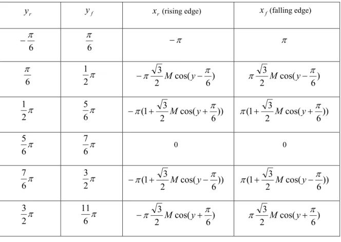
where Vph is the amplitude of the phase voltage. Table 2-1 [42] and table 2-2 show the outer and inner double Fourier integral limits for SVM and DPWM respectively.
Table 2-1 Double Fourier Integral Limits for SVM (Phase A)
r
y yf xr (rising edge) xf(falling edge)
0 3 π )] 6 cos( 2 3 1 [ 2 π π + − − M y )] 6 cos( 2 3 1 [ 2 π π + − y M 3 π π 3 2 ] cos 2 3 1 [ 2 + M y −π cos ] 2 3 1 [ 2 + M y π π 3 2 π )] 6 cos( 2 3 1 [ 2 π π + + − M y )] 6 cos( 2 3 1 [ 2 π π + + y M 3 π − 0 )] 6 cos( 2 3 1 [ 2 π π + + − M y )] 6 cos( 2 3 1 [ 2 π π + + y M π 3 2 − 3 π − cos ] 2 3 1 [ 2 + M y −π cos ] 2 3 1 [ 2 + M y π π − π 3 2 − )] 6 cos( 2 3 1 [ 2 π π + − − M y )] 6 cos( 2 3 1 [ 2 π π + − y M
Table 2-2 Outer and Inner Double Fourier Integral Limits for DPWM (Phase A)
r
y yf xr (rising edge) xf(falling edge)
6 π − 6 π −π π 6 π π 2 1 ) 6 cos( 2 3 π π − − M y ) 6 cos( 2 3 π π M y− π 2 1 π 6 5 )) 6 cos( 2 3 1 ( π π + + − M y )) 6 cos( 2 3 1 ( π π + M y+ π 6 5 π 6 7 0 0 π 6 7 π 2 3 )) 6 cos( 2 3 1 ( π π + − − M y )) 6 cos( 2 3 1 ( π π + M y− π 2 3 π 6 11 ) 6 cos( 2 3 π π + − M y ) 6 cos( 2 3 π π M y+ 0 0.5 1 1.5 2 x 10⁵ 0 50 100 150 200 250 300 350
spectrum of the phase leg PWM voltage for SVM
frequency (Hz) am pl itu de of h ar m oni cs (V )
0 0.5 1 1.5 2 x 10⁵ 0 50 100 150 200 250 300
350 spectrum of the phase leg PWM voltage for DPWM
frequency (Hz) am pl itude of harm on ic s (V )
Figure 2-3 Spectrum analysis for DPWM
Assuming ideal switching behaviors, we can obtain the noise voltage spectrum for a given modulation scheme based on the data of the two tables. Figure 2-2 and Figure 2-3 show the noise spectrum results for a sample three-phase boost rectifier running at 650V DC link voltage and 40 kHz switching frequency with space vector modulation scheme (SVM) and 60° discontinuous pulse width modulation scheme (DPWM) respectively [42]. As we can see, the amplitudes of the first switching harmonic and its adjacent side band for DPWM are higher than those of SVM. But the amplitudes of the high order harmonics for DPWM decrease more quickly than SVM. It indicates that DPWM will cause higher switching current ripple. From the EMI point of view, if the switching frequency is lower than 150 kHz, which is the starting point for radio frequency conducted emission requirement, DPWM will lead to lower EMI noise level as it has lower high order harmonic component. In the applications with SiC devices, the switching frequency of tens of kilo Hertz can be achieved. The low-frequency harmonics caused by switching is not a concern, so DPWM is favored as it has better EMI noise
performance and lower semiconductor loss compared to SVM. All the following analysis in this work is based on DPWM.
With the phase-leg voltage spectrum differential mode (DM) and common mode (CM) noise can be extracted as
3 c b a CM V V V V = + + (2-3) CM c b a DM V V V = ( ,,)− (2-4) where V(a,b,c) is the phase-leg voltage spectrum, VCM and VDM are the CM and DM noise
respectively.
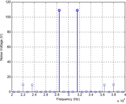
Figure 2-4 and Figure 2-5 show the DM and CM noise spectrum. Figure 2-6 shows the relationship obtained between the required filter corner frequency [43] (a two-stage filter with 80 dB attenuation is assumed, as shown in Figure 2-7) and the switching frequency based on the DO-160E standard [44], which defines the maximum power line noise current as 53 dBµA at 150 kHz. For simplicity, the terminal impedance of the LISN is assumed to be 50 Ω in this analysis. A higher filter corner frequency is desirable since it indicates a smaller filter. The non-monotonous relationship in Figure 2-6 indicates that higher switching frequencies do not necessarily lead to higher filter corner frequencies, unless the switching frequencies are beyond 300−500 kHz. Clearly, there are some preferred switching frequencies, from the standpoint of input EMI filters, as can be seen in Figure 2-6: below 40 kHz, 70 kHz, 140 kHz, or above 300-500 kHz.
104 105 106 0 5 10 15 20 25 30 35 40 45 50
DM noise of the phase leg
Frequency (Hz) dB A bov e 1 V ol t
Figure 2-4 Differential mode noise
104 105 106 0 5 10 15 20 25 30 35 40 45 50
CM noise of the phase leg
Frequency dB A bov e 1 V ol t
Figure 2-5 Common mode noise
Similar relationships can be established for other voltage levels, other topologies, or different filter structures. In final switching frequency determination, the impacts on the boost inductor and the loss should be also included. The result will vary with the given specs, and will also depend on which factor plays the dominant role. As can be seen in
the later sections, the impact of EMI filter is dominant compared to the harmonics filter under the conditions studied in this dissertation.
Figure 2-6 Corner frequency vs. switching frequency
Figure 2-7 Two-stage EMI filter
Figure 2-6 indicates that if the switching frequency is lower than 40 kHz, the EMI filter size will decrease while the switching frequency decreases. But at the same time the required boost inductance will increase due to the higher switching current ripple. In
0 50 100 150 200 250 300 350 400 450 500 10 15 20 25 30 35 40 Switching frequency (kHz) F ilt er c orn er f req ue nc y (k Hz )
Two-stage fitler corner frequency versus switching frequency
DM filter CM filter
addition, the power quality standard defines the harmonic current requirement which is usually specified in the range up to 40 times of the fundamental frequency.
Table 2-3 Harmonic Current Limits
For example, Table 2-3 shows the current harmonic limits for the aircraft [44], where I1 is the amplitude of the fundamental component. Given the 400-800 Hz fundamental
frequency range, the limit is defined up to 32 kHz. If the switching frequency locates in this region the switching ripple current also needs to meet the power quality standard, which brings additional requirement for the filter design. Assuming the same filter structure, Cx1 will not have much impact on the harmonic performance since the source
impedance is usually much lower compared to the capacitor in this frequency range. Therefore the input filter is simplified to a LCL structure for the low frequency current harmonics. The relationship between the harmonic amplitude and the filter parameters is
given by (2-5), where Ik and uk is the amplitude of the kth current and voltage harmonic respectively. LC L u Ih h 2 2 ω ω ⋅ − = (2-5)
uk can be achieved by the spectrum analysis. In this case, the DM noise spectrums
around the first order switching frequency are dominant. Figure 2-8 shows the DM noise of the first order switching frequency for the case of 30 kHz with 800 Hz fundamental frequency. As can be seen, the second order side band is much higher than the other side band harmonics and therefore it will determine the filter size. On the other hand, as far as the switching frequency is much higher than the fundamental frequency, the amplitude of the spectrum will not change with the frequency. We can use the same amplitude value for uk when doing the calculation for different operation point. Then with (2-5) we can
obtain the required inductance for a given harmonic limit. Figure 2-9 shows the required inductance versus switching frequency while assuming the capacitance to be 1 μF. For comparison the inductance to meet EMI requirement is also shown in the same figure. As can be seen, the required inductance increases dramatically once the switching frequency enters the range defined by the power quality standard. Although the lower switching frequency can improve the efficiency and reduce the heatsink, the total system size may still increases due to the tremendous increase of the inductors.
Therefore the low switching frequency boundary is selected to be 40 kHz to avoid relatively low-order harmonics, given the 400-800 Hz fundamental frequency range. For a different design spec, a lower or higher switching frequency range may be selected.
2 2.2 2.4 2.6 2.8 3 3.2 3.4 3.6 3.8 4 x 10⁴ 0 20 40 60 80 100 120 Frequency (Hz) N oi se V ol tag e ( V )
Figure 2-8 DM noise spectrum around the first order switching frequency
20 22 24 26 28 30 32 34 36 38 40 0 200 400 600 800 1000 1200 Switching Frequency (kHz) Induc tanc e (uH ) Inductance required by PQ Inductance required by EMI
2.2.2 Boost Inductor and DC-Link Capacitor Design A. Boost Inductance
When determining the boost inductance, considerations are needed for AC current harmonics, maximum ripple and inrush current. THD can be obtained with the spectrum analysis results under a given switching frequency. It is given by
1 2 ) ( I L u THD i i
∑
= ω (2-6) where ui is the amplitude of the harmonic voltage with order i, ωi is the harmonicfrequency, L is the harmonic inductor and I1 is the fundamental current.
Another consideration for the boost inductance design is the instantaneous switching ripple. It should be suppressed into a reasonable level to guarantee the control feasibility and the proper operation of the switching device [45]. The current ripple will vary as the mains input voltage varies over a fundamental cycle. Here we only discuss the point when the fundamental phase current reaches the peak value as it is important for the inductor physical design. The peak current can be approximated by:
L V T M i ipeak m ) s a/ 4 3 1 ( 2 1 − + = (2-7) where M is the modulation index, im is the amplitude of the fundamental phase current, Ts
is the switching cycle and Va is the voltage of phase A at that instant. Considering the
worse case, the possible minimum modulation index and maximum peak phase voltage should be utilized in (2-6).
During the inrush period, the rectifier works like a diode bridge, the peak current should be constrained due to the limit of the semiconductor device. The relationship between the peak inrush current ipeak and the passive parameters is given by
2 2 2 4 3 ) ( 2 1 m initial Line peak CV V LI Li = − + (2-8) where Vline is the line-to-line voltage, Vinitial is the initial voltage of the DC link cap when
the inrush occurs, and Im is the amplitude of the line current. With (2-6), (2-7) and (2-8),
we can determine the minimum line inductance for the given current requirement.
Actually the boost inductor can also be a part of the EMI filter. So the total input inductance should be the larger one between the two values designed for the EMI filter and the line inductor respectively. Therefore the input filter can be designed as one entity to achieve both harmonic filtering and EMI suppression. For high switching frequency cases, the required harmonic attenuation is small. There is an opportunity to use only EMI filter as the whole input filter since the leakage inductance of the common mode choke is big enough to meet also the harmonic requirement.
B. DC Link Capacitance
For the DC link capacitors selection, considerations are needed for energy storage and system stability.
DC link capacitor is utilized to maintain the DC link voltage for robustness consideration and operation requirement. From the energy point of view, only extreme cases are considered for simplicity. We assume in one switching cycle the rectifier input power is zero while the inverter output power reaches maximum and vice versa. The relationship between the capacitance and the voltage dip is given by
sw dc U U f V P C ) 2 1 ( 2 max Δ ± Δ = (2-9)
where fSW is the switching frequency, U0 and ΔU denote the DC link voltage and voltage
Figure 2-10 Cascaded subsystem diagram out dc P V R 2 = − C ω 1
Figure 2-11 Impedance bode plot
Another concern for the DC link capacitor is the system stability. The rectifier and the inverter are two cascaded subsystems, as shown in Figure 2-10. In order to avoid the interaction between the two systems the output impedance of the rectifier should be lower than the input impedance of the inverter [46]. Figure 2-11 illustrates the impedance relationship in bode plot. The inverter can be considered as a constant power load. And we assume that the output impedance is very low in the control bandwidth while the DC link capacitor is dominant outside the bandwidth. Then the constraint for DC link capacitance is given by m BW out dc Z C f P V ) 2 1 lg( 20 ) lg( 20 2 ≥ − π (2-10)
where fBW is the control bandwidth, Zm is the impedance margin. Then we can decide the
minimum capacitance by (2-9) and (2-10) with the specific system requirement.
In addition to the capacitance, the rms current stress is very important for the capacitor selection as it determines the actual number of capacitors required to be connected in parallel. For voltage source converter, the analytical calculation of rms current stress on the DC link is given by [47]
)] 16 9 3 ( cos 4 3 [ 2 M M I Ilink = M + − π θ π (2-11) where M is the modulation index, IM is the amplitude of the phase current and θ is the
power factor angle. Then the rms current stress on the capacitor can be approximated by
2 _ 2
_rec link inv link
C I I
I = + (2-12) C. Failure Mode Consideration
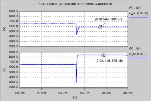
The parameters of the passive components will also impact the failure mode performance of the system. Figure 2-12 shows the switch short failure simulation results with the DC capacitance of 10uF and 100 µF respectively (line inductance is 100 µH for both cases). All other switches are assumed to open after the failure is detected, and the input side circuit breaker to open when the phase current crosses zero. As can be seen from the figures, the DC link voltage in 10 µF case is much higher, extra DC link protection is needed, which will increase the cost and weight of the system. Usually, lower line inductance and higher DC link capacitance can decrease the peak of the over voltage in DC link under failure modes. When designing passive components for a converter, this impact should be taken into consideration.
Figure 2-12 Failure mode comparison for 10uF and 100uF DC link capacitance
Figure 2-13 Circuit diagram for Vienna rectifier
2.2.3 Simulation Verification
In order to verify the design concept developed in this work, a three-phase Vienna type rectifier simulation model is built in Saber. The circuit diagram is shown in Figure 2-13. The parasitic capacitance from the bus to the ground is not considered in this simulation. For the EMI measurement, a 50 Ω LISN is assumed.
Table 2-4 Operation Conditions and Design Results
Source voltage 230V (line to neutral, rms) Source frequency 400Hz
DC link voltage 650V Switching frequency 70kHz
DC Load 10kW constant power load
CM inductor 8mH
DM inductor 100µH
DM capacitor 1µF
CM capacitor 10nF
Damping resistor 1Ω DC link capacitor 40µF/each
Figure 2-14 Simulation results for load step change (The top traces are the capacitor voltages, the bottom traces are the source input current.)
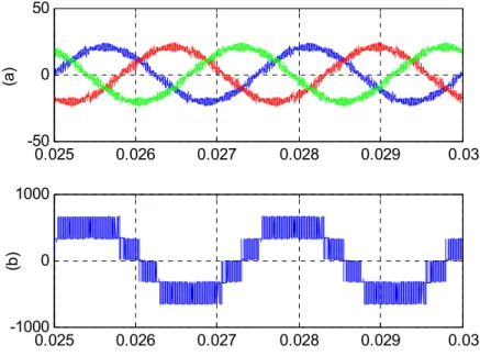
The operation conditions are shown in Table 2-4. The switching frequency is chosen to be 70 kHz according to the EMI considerations described in the previous section. Figure 2-14 shows the simulation results for a constant power load stepping from 5 kW to 10 kW. The results indicate that the system is stable with the designed passive parameters.
0.02 0.022 0.024 0.026 0.028 0.03 -40 -20 0 20 40 (A ) 0.02 0.022 0.024 0.026 0.028 0.03 320 325
330 source current and DC voltage for 10kW
Time (s)
(V
)
Figure 2-15 Steady state simulation waveforms (The top traces are the input currents, the bottom traces are the capacitor voltages.)
Figure 2-16 Harmonic current spectrum
Figure 2-17 EMI spectrum
105 106 -40 -20 0 20 40 60 80 100
Phase current EMI spectrum
(d Bu A) Frequency (Hz) Spectrum EMI Standard 0 2000 4000 6000 8000 10000 12000 14000 16000 0 0.1 0.2 0.3 0.4 0.5 0.6 0.7 0.8 0.9
Current spectrum of 10kW case
Frequency (Hz)
(A
)
Spectrum PQ Standard
The full power steady state waveform is shown in Figure 2-15. The harmonic spectrum analysis results of the input current as well as the power quality standard are shown in Figure 2-16. The EMI spectrum analysis results and the standard requirement are shown in Figure 2-17. The simulation results show that the converter designed parameters meet the standard.
2.3 Summary
The design considerations and procedures to minimize the passive components of the back-to-back VSC converter system are discussed and developed in this chapter. The impact of the switching frequency on the filter corner frequency is studied by the spectrum analysis. It shows that the relationship is non-monotonous. Higher switching frequency will not necessarily lead to smaller EMI filter. Some preferred operating points are determined. Then the lower bound for the line inductance is derived with the current ripple requirement under a given switching frequency. The concept of using the same inductor for boost function and EMI suppression is introduced in the design. Energy storage and impedance interaction requirement are set up to determine the minimum DC link capacitor. The current stress on the DC link cap and the failure mode impact are also discussed. With the principles developed in this chapter, component parameters and switching frequency selection can be traded off in order to achieve minimum passives. The design approach is verified by simulation.
Chapter 3
Topology Evaluation
This chapter presents a methodology to evaluate the three-phase ac topologies with the metric of minimum weight [48]. The approach for passive filter selection developed in Chapter 2 is applied when comparing different topologies. All major components and subsystems in a converter are considered and the interdependence of all the constraints and design parameters is systematically studied. The key design parameters, including switching frequency, modulation scheme, and passive values, are selected considering their impacts on loss, harmonics, electromagnetic interference (EMI), control dynamics and stability, and protection. In this chapter four popular topologies are compared with the proposed methodology.
3.1 Introduction
The power stage design clearly depends on the converter circuit topology. Therefore to achieve a high-density design, it is a logical and necessary step to carry out the systematic design and evaluation for the topologies that meet the application requirements, and select among them the most suitable candidate.
For three-phase ac-ac converters, such as industrial motor drives, the two-level PWM voltage source inverters with 6-pulse diode front-end rectifier has become the topology of choice, due to its simplicity and relatively low cost. One drawback of the diode front-end topology is the low order, low frequency harmonics on the dc link and ac input line, which consequently requires bulky dc-link capacitor and inductor (ac or dc) filters. In order to improve converter performance and achieve higher power density, many
topologies for three-phase ac-ac converters or motor drives with active front-end rectifiers have been proposed and studied [49-57]. These topologies can generally operate with reduced passive components and improved input current wave form. On the other hand, they may have increased loss and electromagnetic interference (EMI) noise, requiring additional cooling and filtering [38]. Different active front-end topologies have different loss, harmonics, and EMI characteristics, which often have contradictory impact on the size and performance of the converter. To achieve a high power density design for a specific application, comprehensive analysis and evaluation are needed to obtain an optimal converter topology selection.
There has been considerable work on ac converter topologies evaluation. The previous work generally focused on specific aspects of the converter design. For instance, [58] compared the steady-state current and voltage waveforms as well as the harmonics injected to the grid for two inverter topologies; [16] discussed device losses, input filter and cost for three-level voltage source converters; [13] [14] [59] evaluated different converter systems in terms of the grid-side power quality and loss distribution; [15] compared the efficiency of the current source and the voltage source drive systems. However, when developing a new converter for high-density applications, all aspects contributing to the converter size and weight must be examined in the design, which requires the correlation between all major design parameters be clearly established. There is a clear need then for a systematic evaluation methodology considering the strong interdependence of all design variables and constraints. For example, increasing switching frequency generally helps to reduce the passive size, but it also increases the converter switching loss and therefore heatsink size. As will be shown later in the chapter,
![Figure 1-3 Switching loss comparison between Si-pin diode and SiC Schottky diode [9]](https://thumb-us.123doks.com/thumbv2/123dok_us/10098849.2910323/19.918.146.778.114.555/figure-switching-loss-comparison-diode-sic-schottky-diode.webp)