Robust Reversible Multiplexer Design using
Mach-Zehnder Interferometer
M.Zaheer Ahmed
#1, S.Md.Imran Ali
#2, P.Nagashyam
#3,T.S.D.V.Subbarao
#4 #Assistant Professor,#Assitant Professor,#UG student,#UG student BITS-KNL,India
---***---Abstract -
Low-power design techniques has anincreased emphasis with the advancements in semiconductor technology over the last few decades. Reversible computing has been proposed by several researchers as a possible alternative to address the energy dissipation problem. Adiabatic logic, nuclear magnetic resonance, optical computing are the implementation alternatives for reversible logic circuits that have been explored in recent years.Recently researchers have proposed implementations of various reversible logic circuits in the all-optical computing domain. Most of these works are based on semiconductor optical amplifier (SOA) based Mach-Zehnder interferometer (MZI), which provides desirable features like low power, fast switching and ease of fabrication. In this paper we present an all-optical implementation of a digital multiplexer using MZI switches. Both non-reversible and reversible versions of multiplexer design are proposed, along with analytical evaluation of the design complexities both in terms of delay and resource requirements. The final optical netlists obtained have been compared against traditional reversible synthesis approaches, by using an available synthesis tool and then mapping the reversible gates to MZI switch based implementations.
1.INTRODUCTION
Reversible logic is becoming a popular emerging paradigm because of its applications in various emerging technologies like quantum computing, DNA computing, optical computing,etc. It is also considered as an alternate low-power design methodology. A reversible circuit consists of a cascade of reversible gates without any fanout or feedback connections, and the number of inputs and outputs must be equal. There exists various ways by which reversible circuits can be implemented like NMR technology, optical technology, etc.In the optical domain, a photon can store information in a signal having zero rest mass and provide very high speed. These properties of photon have motivated researchers to study and implement reversible circuits in optical domain. Theoretically from the decade old principles of Landauer and Bennett , reversible logic is considered as a potential of reversible gates can be one possible alternative to
overcome the power dissipation problem in conventional computing. In recent times researchers have investigated various reversible logic gates and their all-optical implementations using microresonator and semiconductor optical amplifier (SOA) based Mach-Zehnder interferometer (MZI) switch. Also MZI-based implementation of reversible logic gates offer significant advantages like ease of fabrication, high speed, low power, and fast switching time. In this paper, an all-optical implementation methodology of reversible multiplexers has been proposed. Delay analysis in implementing arbitrary functions using such multiplexers have also been discussed.
2.LITERATURE SURVEY
In this section we briefly discuss some relevant background about MZI-based optical switch, various reversible gates, and their all-optical implementations.
A. MZI-based all-optical switch
• When both incoming signal (λ1) at A and control signal (λ2) at B are present, there will be a presence of light at bar port and no light at cross port.
• When there is incoming signal (λ1) at A and no control signal (λ2) at B, then there is absence of light at bar port and
presence of light at cross port.
Figure: SOA based MZI switch C.Implementing reversible gates using MZI switch
Several researchers have studied and proposed all-optical implementations of reversible and non-reversible gates like Toffoli, Fredkin, Peres, XOR, NOR, etc, and some function implementations like adder [9] and signed adder [1]. In all the works, the optical cost of implementation has been estimated as the number of MZI switches required, since the costs of beam splitters and beam combiners are relatively small. And the delay has been calculated as the number of stages of MZI switches multiplied by a unit Δ.
3.PROPOSED ALL-OPTICAL MULTIPLEXER DESIGN
In this section, we present the all-optical implementation of a digital multiplexer using MZI switches, beam splitters and beam couplers. In the following subsections, we discuss the design of a (2 × 1) non-reversible all-optical multiplexer, followed by its generalization to (2n ×1) multiplexer. Then a design extension to make the multiplexer design reversible is suggested, that requires one additional ancilla line.
A. Design of (2 × 1) multiplexer
The schematic diagram of a (2 × 1) multiplexer is shown in Figure 4(a), where I0 and I1 are the two inputs, and S is the select line. The function implemented at the output is also shown.
The all-optical implementation of the multiplexer is shown in Figure 4(b), which consists of a beam splitter (BS) for splitting the select input S, two MZI switches which generates the sub functions I0.S, I0.S_, S.I1 and S.I_1 respectively, and finally a beam coupler (BC) that combines two of the MZI outputs to realize the desired functionality at the final output F. The BC essentially performs the logical OR function in the digital domain.
In the earlier reported works on implementing logic functions using MZI switches, BS and BC [8], [9], the cost of implementation (referred to as optical cost) has been estimated as the number of MZI switches required, as the relative costs of BS and BC are small. Similarly, the delay is measured as the length of the longest cascade of MZI switches. Denoting the units of cost and delay by MZI and Δ, for the implementation as shown in Figure 4(b),
M(1) = 2 MZI
D(1) = 1 Δ
where M(x) and D(x) respectively denote the optical cost and delay for a (2x × 1) multiplexer.
Figure: A 2- to-1 MUX
B. Design of (2n × 1) multiplexer
We now show how a multiplexer of any larger size can be constructed using smaller multiplexers as basic building blocks. This is a standard approach followed in conventional logic design; however, in the context of the present work, we shall be analyzing the costs and delays with respect to the all-optical implementations.
A (4×1) multiplexer can be constructed using three
final netlist as shown in Figure For this implementation,
M(2) = 6 MZI
D(2) = 2 Δ
Figure: Schematic diagram of 4-to-1 MUX
Similarly, an (8 × 1) multiplexer can be built using two (4 × 1) and one (2 × 1) multiplexers, for which
M(3) = 6 * 2 + 2 = 14 MZI
D(3) = 3 Δ
Generalizing, an (2n × 1) multiplexer can be built using two (2n−1 × 1) and one (2 × 1) multiplexers. We have seen earlier that M(1) = 2, M(2) = 6, and M(3) = 14. We can express the optical cost M(n) as a recurrence relation and solve it as follows
M(n) = 2.M(n − 1) +M(1)
= 2.M(n − 1) + 2
= 2[2.M(n − 2) + 2] + 2= 22.M(n − 2) + 22 + 2
= 22[2.M(n − 3) + 2] + 22 + 2
= 23.M(n − 3) + 23 + 22 + 2
...
= 2n−1.M(1) + 2n−1 + 2n−2 + · · · + 2
= 2n + 2n−1 + · · · + 2
= (2n+1 − 2) MZI (1)
Since the number of MZI stages is equal to the number of multiplexer select lines in the final netlist, we can write the delay for an (2n × 1) multiplexer as
D(n) = n Δ (2)
C. Reversible implementation of the multiplexer
The all-optical implementations of multiplexer as discussed in the previous subsection are not reversible. One possible approach to have a reversible implementation of a multiplexer is to define a suitable reversible embedding for a (2 × 1) multiplexer, and use it to build larger multiplexers.
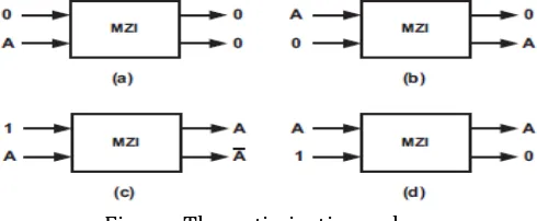
A.Optimization rules
It may be observed that in the all-optical multiplexer-based realization of functions, some of the MZI switches have constant inputs (0 or 1). Some of these MZI switches may be eliminated from the final netlist. These may be summarized in terms of the following four optimization rules.
a) If the upper input of a MZI switch is 0, both the outputs will be 0’s and the switch can be deleted from the netlist.
b) If the lower input of a MZI switch is 0, the upper output will also be 0, and the upper input will get copied to the lower output. In this case also, the MZI switch can be deleted
c) If the upper input of a MZI switch is 1, the two outputs will be respectively the lower input and its complement. A MZI switch in this configuration can be used as an Inverter
[image:3.595.319.564.585.686.2]d) If the lower input of a MZI switch is 1, the upper input gets copied to the upper output, and the lower output becomes 0. Here again the switch can be deleted.
Figure: The optimization rules
4.EXPERIMENTAL RESULTS
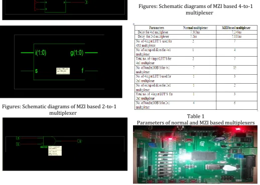
represent the schematic diagrams of MZI based 2-to-1 &4-to-1 mutiplexers.
It may be noted that the delay as reported in table for the proposed approach uses a straightforward multiplexer based realization without using the optimization rules as discussed in the previous section. If the rules are used, significant reductions in the number of MZI switches are expected. The table shows that the optical costs for some of the benchmarks are less in the proposed approach, while for some others it is more. However, the delays are significantly less for all the benchmarks in the multiplexer based approach.
Figures: Schematic diagrams of MZI based 2-to-1 multiplexer
[image:4.595.43.562.371.740.2]Figures: Schematic diagrams of MZI based 4-to-1 multiplexer
Table 1
Parameters of normal and MZI based multiplexers
5. CONCLUSION
In this paper all-optical implementation of multiplexers using Mach-Zehnder Interferometer (MZI) based switches have been presented, along with analysis of the corresponding costs and delays. Using one ancilla line, a reversible implementation of multiplexer is also proposed. A method for reversible implementation of functions using MZI switches and some optimization rules have also been presented.
Experimental results for some of the benchmarks reveal that the proposed all-optical implementation results in significantly less delay as compared to the one based on conventional reversible gate implementations. Comparison with a recent work for the 13 standard 3-variable functions has also been reported, which demonstrates significant improvements both in terms of optical cost and delay.
6.REFERENCES
[1] A. Al-Zayed and A. Cherri. Improved all-optical modified signed digit adders using semiconductor optical amplifier and Mach-Zehnder interferometer. Optics and Laser Technology, 42(5):810–818, 2010.
[2] C. Bennett. Logical reversibility of computation. Journal of IBM Research and Development, 17:525–532, 1973.
[3] T. Chattopadhyay. All-optical symmetric ternary logic gate. Optics and Laser Technology, 42(6):1014– 1021, 2010.
[4] T. Chattopadhyay. All-optical modified Fredkin gate. IEEE Journal of Selected Topics in Quantum Electronics, 18(2):585–592, 2012.
[5] R. Feynman. Quantum mechanical computers. Optic News, 11:11–20, 1985.
[6] E. Fredkin and T. Toffoli. Conservative logic. Inernational Journal of Theoretical Physics, 21:219–253, 1982.
[7] J. Kim, J.-S. Lee, S. Lee, and C. Cheong. Implementation of the refined Deutsch-Jozsa algorithm on a three-bit NMR quantum computer. Physical Review A (Atomic, Molecular, and Optical Physics), 62(5):27– 37, 2000.
[8] S. Kotiyal, H. Thapliyal, and N. Ranganathan. Mach-Zehnder interferometer based all optical reversible
NOR gate. In Proc. of IEEE Computer Society Annual Symposium on VLSI, pages 207–212, 2012.
[9] S. Kotiyal, H. Thapliyal, and N. Ranganathan. Mach-Zehnder interferometer based design of all optical reversible binary adder. In Proc. Of Design, Automation and Test in Europe (DATE), pages 721–726, 2012.