UNIVERSITY OF GENOVA
Polytechnic School
Doctoral Program in Science and Technology for Electronic and Telecommunication Engineering (XXXII cycle)
Energy-efficient embedded machine learning algorithms for
smart sensing systems
Mario Osta
Supervisor: Prof. M. Valle
A thesis submitted for the degree of Doctor of Philosophy
ACKNOWLEDGMENTS
This Ph.D. journey is a combined effort of several individuals, including the scholars, family members who supported me, and friends who were always accessible through this journey.
First and foremost, I would like to express my gratitude to my marvelous thesis supervisor Prof. Maurizio Valle whose support, guidance during these three years has made this thesis possible. He gave me opportunities to improve my work through my learning path.
I am very grateful to my colleague Dr. Ali Ibrahim for his encouragement and extensive support through my Ph.D. journey. His evaluation and suggestions were essential to solving various bottlenecks in my research work innovatively. He influenced me to work hard and persist in my determination.
During my Ph.D., I had the opportunity to work at the Swiss Federal Institue of Technology in Zurich (ETH) as a visiting researcher. I am grateful to my internship mentor for making this research work successful.
I would like to thank my friends and lab mates at the COSMIC lab for the lively discussion and unforgettable adventures. I am also grateful to all my friends at the ETH IIS lab in Zurich.
Last but not least, I would also like to thank my parents, my sister, and my brother, for their advice and support throughout my life. This could not be achieved without them.
SUMMARY
Embedded autonomous electronic systems are required in numerous application domains such as Internet of Things (IoT), wearable devices, and biomedical systems. Embedded electronic systems usually host sensors, and each sensor hosts multiple input channels (e.g., tactile, vision), tightly coupled to the electronic computing unit (ECU). The ECU extracts information by often employing sophisticated methods, e.g., Machine Learning. However, embedding Machine Learning algorithms poses essential challenges in terms of hardware resources and energy consumption because of: 1) the high amount of data to be processed; 2) computationally demanding methods. Leveraging on the trade-off between quality requirements versus computational complexity and time latency could reduce the system complexity without affecting the performance. The objectives of the thesis are to develop: 1) energy-efficient arithmetic circuits outperforming state of the art solutions for embedded machine learning algorithms, 2) an energy-efficient embedded electronic system for the “electronic-skin” (e-skin) application. As such, this thesis exploits two main approaches:
Approximate Computing: In recent years, the approximate computing paradigm became a significant major field of research since it is able to enhance the energy efficiency and performance of digital systems. “Approximate Computing”(AC) turned out to be a practical approach to trade accuracy for better power, latency, and size [1],[2]. AC targets error-resilient applications and offers promising benefits by conserving some resources. Usually, approximate results are acceptable for many applications, e.g., tactile data processing [3], [4] image processing [5], and data mining [6]; thus, it is highly
recommended to take advantage of energy reduction with minimal variation in performance [7]. In our work, we developed two approximate multipliers: 1) the first one is called “META” multiplier and is based on the Error Tolerant Adder (ETA), 2) the second one is called “Approximate Baugh-Wooley(BW)” multiplier where the approximations are implemented in the generation of the partial products. We showed that the proposed approximate arithmetic circuits could achieve a relevant reduction in power consumption and time delay around 80.4% and 24%, respectively, with respect to the exact BW multiplier. Next, to prove the feasibility of AC in real world applications, we explored the approximate multipliers on a case study as the e-skin application. The e-skin application is defined as multiple sensing components, including 1) structural materials, 2) signal processing, 3) data acquisition, and 4) data processing. Particularly, processing the originated data from the e-skin into low or high-level information is the main problem to be addressed by the embedded electronic system. Many studies have shown that Machine Learning is a promising approach in processing tactile data when classifying input touch modalities. In our work, we proposed a methodology for evaluating the behavior of the system when introducing approximate arithmetic circuits in the main stages (i.e., signal and data processing stages) of the system. Based on the proposed methodology, we first implemented the approximate multipliers on the low-pass Finite Impulse Response (FIR) filter in the signal processing stage of the application. We noticed that the FIR filter based on (Approx-BW) outperforms state of the art solutions, while respecting the tradeoff between accuracy and power consumption, with an SNR degradation of 1.39dB. Second, we implemented approximate adders and multipliers respectively into the Coordinate Rotational Digital Computer (CORDIC) and the Singular Value Decomposition (SVD)
circuits; since CORDIC and SVD take a significant part of the computationally expensive Machine Learning algorithms employed in tactile data processing. We showed benefits of up to 21% and 19% in power reduction at the cost of less than 5% accuracy loss for CORDIC and SVD circuits when scaling the number of approximated bits.
2) Parallel Computing Platforms (PCP): Exploiting parallel architectures for near-threshold computing based on multi-core clusters is a promising approach to improve the performance of smart sensing systems. In our work, we exploited a novel computing platform embedding a Parallel Ultra Low Power processor (PULP), called “Mr. Wolf,” for the implementation of Machine Learning (ML) algorithms for touch modalities classification. First, we tested the ML algorithms at the software level; for RGB images as a case study and tactile dataset, we achieved accuracy respectively equal to 97% and 83.5%. After validating the effectiveness of the ML algorithm at the software level, we performed the on-board classification of two touch modalities, demonstrating the promising use of Mr. Wolf for smart sensing systems. Moreover, we proposed a memory management strategy for storing the needed amount of trained tensors (i.e., 50 trained tensors for each class) in the on-chip memory. We evaluated the execution cycles for Mr. Wolf using a single core, 2 cores, and 3 cores, taking advantage of the benefits of the parallelization. We presented a comparison with the popular low power ARM Cortex-M4F microcontroller employed, usually for battery-operated devices. We showed that the ML algorithm on the proposed platform runs 3.7 times faster than ARM Cortex M4F (STM32F40), consuming only 28 mW. The proposed platform achieves 15× better energy efficiency than the classification done on the STM32F40, consuming 81mJ per classification and 150 pJ per operation.
TABLE OF CONTENTS
ACKNOWLEDGMENTS ii
SUMMARY iv
LIST OF FIGURES x
LIST OF TABLES xiii
CHAPTER1. Introduction 1
1.1 Introduction 1
1.2 Embedded Machine Learning 3
1.2.1 Power/Energy Consumption………....3
1.2.2 Latency……….4
1.2.3 Memory storage………...4
1.2.4 Algorithm complexity………..5
1.3 Machine Learning On Embedded Hardware Platforms 5
1.4 Energy-Efficient Techniques for ML/DL Processing 6
1.4.1 Parallelism and Data Reuse………..8
1.4.2 Approximations………8
1.4.2.1 Algorithmic Level………...…10
1.4.2.2 Architecture Level………..….11
1.4.2.3 Circuit Level………11
1.4.3 Network Sparsity………...….12
1.5 Context of the Work 12
1.6 Thesis contributions 13
CHAPTER2. Low Power Approximate Arithmetic Circuits 17
2.1 Introduction 17
2.2 Background on Adders and Multipliers 18
2.2.1 Representation of signed integers………...19
2.2.2 Basic Adders………..20
2.2.2.1 Ripple-Carry Adder……….20
2.2.2.2 Carry-Chain Adder………..20
2.2.2.3 Carry-Lookahead Adder……….22
2.2.3 Multiplication……….22
2.2.3.1 Partial Product Generation………..22
2.2.3.2 DADDA Multipliers………23
2.2.3.3 WALLACE Multipliers……….….24
2.2.3.4 Baugh-Wooley Multiplier………..26
2.3Background on Approximate Adders and Multipliers 28
2.3.1 Approximate Adders………..28
2.3.2 Approximate Multipliers………....29
2.4Low Power Approximate Adders and Multipliers 30
2.4.1 Approximate Adders Circuits…….………....31
2.4.2 Approximate Multipliers Circuits…..………....35
2.4.2.1 Approximate META Multiplier……….….36
2.4.2.2 Approximate Baugh-Wooley Multiplier……….42
2.5Results 46
2.5.1 Hardware Implementation of META Multiplier……….54
2.5.2 Hardware Implementation of Approximate Baugh-Wooley Multiplier……..61
2.6Conclusion 61
CHAPTER3. Approximate Computing Circuits for Tactile Data Processing 63
3.1 Introduction 63
3.2.1 Sensor array………...65
3.2.2 Interface electronics………...66
3.2.3 Signal and data processing……….66
3.3 Methodology for Approximating Tactile Sensing 67
3.4 Approximations in Digital Signal Processing 69
3.4.1 Experimental Setup Description……….……69
3.4.2 Finite Impulse Response Filter Structure………70
3.4.3 Filtered Output Tactile Data………..….72
3.5Approximations in Data Processing 73
3.5.1 CORDIC Algorithm…..………....74
3.5.2 CORDIC Circuits………..75
3.5.3 Hardware Implementation of Approximate CORDIC………..….78
3.5.4 Singular Value Decomposition……….……82
3.5.5 Hardware Implementation of Approximate SVD……….….86
3.6Conclusion 92
CHAPTER4. Machine Learning Algorithms for Tensorial Tactile Data Processing 94
4.1 Introduction 94
4.2 Tactile data based on the tensorial approach 95
4.3 Machine Learning Approaches for Touch Recognition 96
4.3.1 Pattern Recognition Based on Kernel Methods……….97
4.3.2 Exploiting Kernel Functions for Tensorial Approach………..101
4.4 Experimental Setup and Results 105
4.4.1 The Model Choice for Touch Recognition………..…105
4.4.2 Dataset………107
4.4.2.1 RGB Image………..107
4.4.2.2 Tactile Data……….108
4.4.3 Data Preprocessing……….……108
4.4.4.1 Image Classification………...109
4.4.4.2 Touch Modalities Classification………...110
4.4.5 Prediction Phase………....111
4.5 Conclusion 112
CHAPTER5. Energy-Efficient System for Touch Modalities Classification 114
5.1 Introduction 114
5.2 PULP processing unit 116
5.2.1 SoC Domain………...………..116
5.2.2 Cluster Domain………...……….119
5.3 SVM based Tensor Kernel Algorithm on the PULP Architecture 120
5.3.1 Inference Implementation………...120
5.3.2 Fixed-Point Implementation………...….123
5.3.3 Parallelization and Memory Management Strategy……….124
5.4 Experimental Results and Performance Assessment 127
5.4.1 Performance………...….128
5.4.2 Power Consumption………..….129
5.5 Conclusion 131
CHAPTER6. Conclusion and future extensions 132
APPENDIX 136
LIST OF FIGURES
1.1 Energy-efficient methods for embedded machine learning………...2
1.2 An overview of some energy-efficient techniques at the algorithmic, architecture, and circuit-level for embedded Machine and Deep Learning Algorithms………...8
2.1 Ripple-carry adder………..…19
2.2 Carry-chain adder……….…..21
2.3 Partial products for unsigned numbers………...………22
2.4 Partial products for two’s complement numbers ………...23
2.5 Dot diagram for an 8×8 DADDA multiplier………...24
2.6 Dot diagram for an 8×8 WALLACE Multiplier……….25
2.7 Block diagram of the Baugh-Wooley multiplier……….26
2.8 General hardware architecture for approximate adder circuits………...30
2.9 Approximate adder circuits………31
2.10 Block diagram of the META approximate multiplier………35
2.11 Block diagram of ETA adder……….36
2.12 Architecture of approximate Baugh-Wooley multiplier………38
2.13 Probability of acceptance versus minimum acceptable accuracy for META and S-MRCA………44
2.14 Probability of acceptance versus minimum acceptable accuracy for META and U-MRCA………...45
2.15 Error percentage distribution for the two approximate multipliers………....46
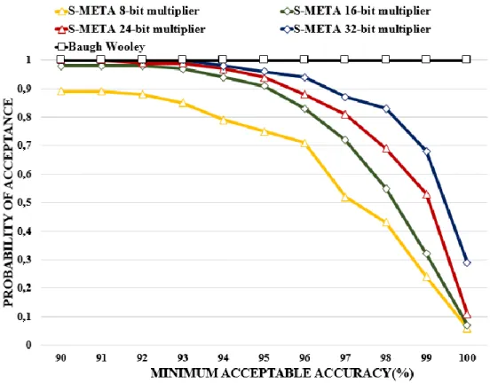
2.16 Probability of acceptance of S-META for different bit sizes……….47
2.17 Probability of acceptance of U-META for different bit sizes………48
2.19 Instantaneous power consumption and delay of META multiplier………...50
2.20 Percentages of outputs versus relative error distance for different inexact multiplier circuits………52
2.21 Variation of NMED(a), MRED(b) and PASS RATES(c) with respect to the number of bits approximate bits………..53
2.22 Power consumption, delay and MRE of exact and approximate multiplier designs………54
3.1 Block diagram of the e-skin system………..……….59
3.2 Sensor array………60
3.3 Proposed methodology for approximate tactile sensing system……….63
3.4 Experimental Setup………65
3.5 a). Functional block diagram for quality evaluation of FIR filter based approximate multiplier b) Design of 16-tap low pass finite impulse response filter using approximate multipliers ……….66
3.6 Sorted signal-to-noise ratio for the exact and approximate multipliers………...67
3.7 Waveforms of tactile signals generated from the sensor array using FIR filters based on approximate multipliers……….68
3.8 Architecture of the CORDIC in rotation mode………...71
3.9 Percentages of outputs versus relative error distance for different inexact adder circuits………73
3.10 Power consumption, delay, and MRE of exact and approximate adder designs…..74
3.11 Approximate SVD block diagram……….76
3.12 Accuracy of the eigenvalues of the approximate SVD for an input matrix of size (5×5)………...77
3.13 Accuracy of the eigenvalues of the approximate SVD for an input matrix of size (8×8)………...78
3.14 Performance and Error resilience analysis of the Singular Value Decomposition for an input matrix of size (5×5) (a) and (8×8) (b)………81
4.2 Support vector machine………..88
4.3 Tensor unfolding………92
4.4 Non-linear SVM………...………...…97
4.5 Sample images……….100
4.6 Touch modalities. (a) Finger sliding; (b) washer rolling………...……101
4.7 Schematic of the algorithm box………....105
5.1 Block Diagram, including the tactile sensor array, the sensor’s interface, and the processing platform……….….107
5.2 High-Level Mr. Wolf architecture………..………108
5.3 Mr. Wolf SoC block diagram………109
5.4 Mr. Wolf cluster block diagram………...….111
5.5 Mr. Wolf Board………..……..112
5.6 Online computation of the SVM based tensor kernel algorithm………..…….117
5.7 L2 memory allocation sequence……….……..122
5.8 Power consumption and energy efficiency comparison of the online computation algorithm on the ARM Cortex M4 and Wolf………...…….126
5.9 Power consumption and energy efficiency of each function of the online computation algorithm on Mr. Wolf………..127
LIST OF TABLES
1.1 Energy-efficient embedded machine/deep learning algorithms on different hardware
platforms………7
1.2 Approximate computing methods at different abstraction levels………....10
2.1 Output of Sum and Carry bits For Different Cases……….….41
2.2 Simulation results of 8-bit multipliers………49
2.3 Accuracy metrics for different approximate multipliers designs………51
2.4 Area, PDP, and PDP-MRED of multipliers designs………...55
3.1 Accuracy Metrics For Different Approximate Adders Designs………..……72
3.2 Full adder versus approximate adders based CORDIC circuits………74
3.3 Percentage relative error of Approximate SVD………..78
3.4 Relative error of the eigenvalues resulted from the approximate SVD for an input matrix of size (8 ×8)………79
4.1 Results of model selection and accuracy obtained for image classification………103
4.2 Results of model selection and accuracy obtained for touch modalities classification………....104
5.1 Characteristics of Mr. Wolf………..……109
5.2 Q16.16 format range……….………120
5.3 Algorithm memory………...……122
5.4 Algorithm memory for different size of tensors………123
5.5 Performance of the tensorial kernel online computation on Wolf platform. Cyc, T, Sp stand for cycles, Time and speed-up……….…125
CHAPTER 1.
INTRODUCTION
1.1 Introduction
Over the past decade, a new wave of intelligent computing systems driven by machine learning algorithms has been deployed in many applications such as the Internet of things and security systems. IoT devices ought to effectively decode a large amount of raw data coming from miniaturized sensors providing vital information. The extracted information is transmitted onto the wireless channel, and it is usually used to close the loop in control systems providing real-time response. Besides, the small size form of these embedded devices (e.g., wearable sensors) limits the battery size and hence the energy availability.
Furthermore, intelligent devices could move “closer to the sensor,” thereby eliminating the latency of cloud access and reducing limitations in communication bandwidth by employing sophisticated methods (e.g., Machine learning). Machine learning is considered as dominant paradigms making intelligent tasks and providing information about the observed phenomenon. However, deploying Machine Learning algorithms in embedded devices poses several challenges in terms of hardware resources and energy consumption because of 1) the high amount of data to be processed significantly affecting the real-time functionality, and 2) the complex processing tasks involve computationally demanding methods imposing an additional burden in terms of power consumption. Therefore, aiming to implement powerful machine and deep learning algorithms within a power range of microwatt requires an essential improvement in processing energy efficiency.
Leveraging on the trade-off between quality versus computational complexity and latency would reduce the system complexity (see Fig.1.1) without affecting the system functionality. Such an approach can be achieved by several energy-efficient techniques (Parallelism and data reuse, Approximate Computing, Network Sparsity) on embedded machine learning systems. In this perspective, this chapter aims to present an overview of the energy-efficient implementation of machine learning algorithms on hardware platforms highlighting the main challenges when embedding such algorithms. Moreover, it reports the techniques that could be applied to improve energy efficiency, such as approximate computing, by reviewing the effective methods used to overcome the challenges at the circuit, architectural, and algorithmic levels. Further, it describes the main factors to be taken into consideration when choosing the appropriate platform. Lastly, this chapter
describes the context of the work and the mains contributions achieved during the Ph.D. The overview work presented in this chapter was published in [129], [131].
1.2 Embedded Machine Learning
Machine learning has emerged in different scientific fields and everyday tasks in today’s electronic systems and smartphones. ML paradigms have been effectively used to address standard regression and classification problems. Furthermore, deep learning methods represent state-of-the-art technology addressing the task of extracting structured information from complex domains such as object/face recognition, object tracking, etc. However, employing such paradigms for embedded platforms imposes challenges in terms of time latency, energy consumption, and storage.
1.2.1 Power/Energy Consumption
Energy consumption is the power consumed during the runtime of the algorithm when targeting embedded implementations. It is the energy consumed during the execution of the algorithm, basically composed of computing energy, IO operations, and necessary energy for memory storage. Energy efficiency is considered an essential metric, especially when dealing with applications such as portable, medical/biomedical IoT devices. Moreover, integrated circuits must embed ML instead of power-hungry FPGA-based microprocessors in order to meet the low power budget constraint in wearable or implantable devices [8],[9]. To emphasize the critical need of this metric, we take an example of the implemented tensorial SVM on the FPGA device for classifying different touch modalities, as shown in [10]. The proposed implementation is feasible for real-time classification while the amount of power consumed is 1.14 W. Similarly, as shown in
[8],[9] ML must be embedded into dedicated platforms in order to reduce the power envelope constraint in wearable devices to the range of mW. Therefore, the critical challenge is to improve power consumption while preserving the real-time constraints for longer battery life. Improving energy efficiency will provide longer battery life, and then more extended functionality within the same energy source.
1.2.2 Latency
Real-time operation is a principal requirement in many application domains for embedded ML[11]. Latency is defined as the time difference between the generated output data and the input data provided to the system. The time latency depends on the number of operations performed in a unit of time, such as operations per second (OPS) or floating-point operations per second (FLOPS). In many real-time applications such as deep brain stimulation[12]and vital sign monitoring[13], the response time of the machine learning algorithm must be adequately fast. Moreover, [14] and [15] ML/DL algorithms take more than 1 second to classify different objects. This fact highlights the latency problem faced in IoT devices when implementing ML/DL algorithms; since the application must meet real-time constraints.
1.2.3 Memory Storage
Memory is a big challenge in embedded machine learning and deep neural networks today[16],[17]. Memory subsystems expend significant time and energy in computing platforms due to the frequent high data transfer between processors and off-chip memory[18]. Researchers are combatting with the DRAM devices having limited capacity and memory bandwidth. The memory is employed for storing a high amount of training
data, and parameters such as weights in DNN and support vectors in SVM. The higher the number of training data, the harder the memory challenge. For example, more than 900M operations of memory read, and writes are needed in [19].
1.2.4 Algorithm Complexity
Concerning the complexity of the algorithm, it depends on the number of mathematical operations and instructions executed by the algorithm in the embedded space. For instance, ANN requires energy consumption less than SVM since the ANN model takes five times fewer operations than SVM [20].
1.3 Machine Learning On Embedded Hardware Platforms
This section describes the steps to follow when implementing ML on embedded hardware platforms [21]. A model with few operations should be selected since some networks, e.g., AlexNet and GoogleNet[22], [23], are not designed for the embedded space. Then, a performance study must be applied on the selected ML algorithm, which depends on some characteristics such as: 1) the number of layers, 2) fps (frames per second) requirements, 3) the number of bits used in the algorithm, 4) memory storage and 5) number of operations. The final step is to look for processors supporting some significant features (e.g., quantization, sparsity, etc.). For example, different software architectures of CNN have been designed in[24] in order to find only one suitable architecture having the lowest complexity.
Moreover, the activation of the hidden layers with the parameters of the selected CNN, which will be implemented, must be regularly stored and accessed. Then, the low power
microcontroller from the MSP430FR series is selected as the target platform. It is characterized by a ferromagnetic memory of 256 kB, which reduces power consumption by three times and increases the speed up of the data movement by 100x. Similarly, in[25], the DNPU processor characterized by a LUT-based multiplier dedicated to quantization is considered optimal for the implementation of CNN and RNN. Thus, reducing off-chip memory access and improving the energy efficiency consequently by 4.5x with a negligible accuracy loss. Therefore, by following the flow diagram, the selected processor will feed the requirements of the selected algorithm, leading to an efficient implementation.
1.4 Energy-Efficient Techniques For ML/DL Processing
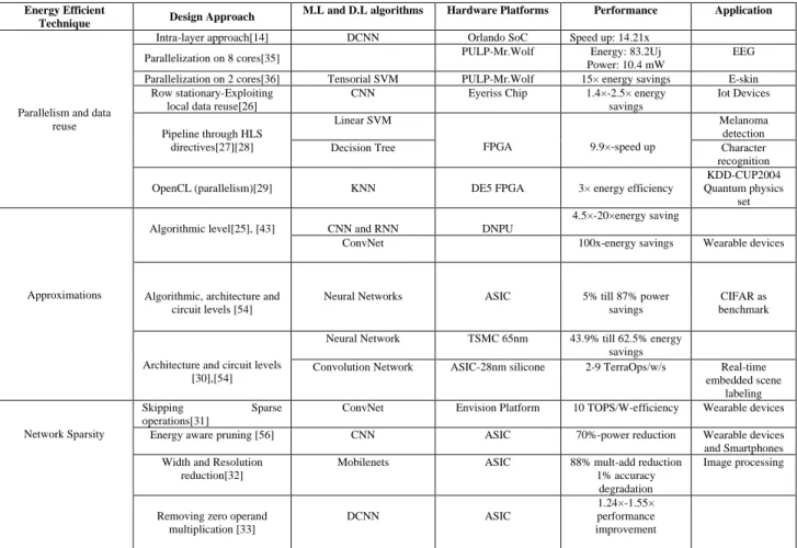
Table 1.1.: Energy efficient embedded machine/deep learning algorithms on different hardware platforms
Energy Efficient
Technique Design Approach
M.L and D.L algorithms Hardware Platforms Performance Application
Parallelism and data reuse
Intra-layer approach[14] DCNN Orlando SoC Speed up: 14.21x Parallelization on 8 cores[35] PULP-Mr.Wolf Energy: 83.2Uj
Power: 10.4 mW
EEG Parallelization on 2 cores[36] Tensorial SVM PULP-Mr.Wolf 15× energy savings E-skin
Row stationary-Exploiting local data reuse[26]
CNN Eyeriss Chip 1.4×-2.5× energy
savings Iot Devices Pipeline through HLS directives[27][28] Linear SVM FPGA 9.9×-speed up Melanoma detection
Decision Tree Character
recognition OpenCL (parallelism)[29] KNN DE5 FPGA 3× energy efficiency
KDD-CUP2004 Quantum physics
set
Approximations
Algorithmic level[25], [43] CNN and RNN DNPU
4.5×-20×energy saving
ConvNet 100x-energy savings Wearable devices
Algorithmic, architecture and circuit levels [54]
Neural Networks ASIC 5% till 87% power savings
CIFAR as benchmark
Architecture and circuit levels [30],[54]
Neural Network TSMC 65nm 43.9% till 62.5% energy savings
Convolution Network ASIC-28nm silicone 2-9 TerraOps/w/s Real-time embedded scene
labeling
Network Sparsity
Skipping Sparse operations[31]
ConvNet Envision Platform 10 TOPS/W-efficiency Wearable devices Energy aware pruning [56] CNN ASIC 70%-power reduction Wearable devices and Smartphones Width and Resolution
reduction[32]
Mobilenets ASIC 88% mult-add reduction 1% accuracy
degradation
Image processing
Removing zero operand multiplication [33] DCNN ASIC 1.24×-1.55× performance improvement 3333333333333333333333
Selecting the appropriate hardware platform can be incorporated with other optimization techniques that could be applied to embedded Machine learning implementations.
Table 1.1 reports some of the most significant energy-efficient techniques employed in the literature at different levels, for embedded ML/DL algorithms on different hardware platforms (FPGA, Parallel platforms, an ASIC). It highlights the use of some relevant techniques by presenting the followed design approach. Then an analysis of the impact of these techniques on different applications is reported. These techniques include (1) Parallelism and data reuse[26],[27],[28],[29] (2) Approximations[30], and (3) Network Sparsity[31],[32],[33] (see fig.1.3). However, the main challenge is to find the optimal way of choosing a technique or a combination of multiple techniques that can be implemented at different abstraction levels.[27] This can further reduce the power/energy consumption while obeying the target application requirements.
Fig.1 Fig.1 Flow diagram of selecting Machine learning algorithms on embedded platforms [9]
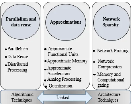
Fig. 1.2. An overview of some energy efficient techniques at algorithmic, architecture and circuit level for embedded Machine and Deep Learning Algorithms
1.4.1 Parallelism and Data Reuse
Parallelism is one of the most used solutions to simplify this challenge. For instance, many computations within the same function of the algorithm can share common resources, as shown in [14], [34]and [35]. Authors in [14] took advantage of the multicore architecture offered by Orlando SoC to parallelize the convolution operations on tensors, achieving a speedup of 14.21x. In [34], [35], the PULP platform, an efficient ultra-low-power processor, is used for EMG signal and nano drones, where power consumption and energy efficiency have been reduced to below 64 mW by utilizing the available eight cores in [34]. Also, in [36], relatively low power consumption less than 28 mW and an energy efficiency improvement of 15x have been recorded when parallelizing the tensorial SVM on two cores of the PULP platform.
1.4.2 Approximations
Due to their inherent error resiliency, machine learning methods may scarify a part of their accuracy at the benefit of performance improvement. In this regard, recent researches have relied on approximate computing methods to address the embedded implementation of ML algorithms. Approximate computing methods have been applied at various levels of the system abstraction, i.e. algorithmic, architecture, and circuit levels. Table 1.2 reports some relevant works presented in the literature at different levels [37]. It highlights the used approximate computing technique and the followed design approach with the analysis of the impact of the results on the application. The analysis is basically focused on the gain in performance represented by the power and latency savings on the one hand, and by the accuracy degradation on the other hand. Approximate Computing (AxC) is the idea of a
trade-off between accuracy and efficiency. It allows the system to expose inexactness to the application layer of an error-resilient system in return for conserving some resources. Therefore, selecting an AxC technique for an embedded machine learning algorithm requires careful analysis in order to maintain a low accuracy degradation with a noticeable reduction in power consumption.
1.4.2.1 Algorithmic Level
At the algorithmic level[38],[39], approximations are applied to the loops and functions constituting the program/software which describes the application. These approaches enable the approximation by reducing the number of iterations in an iterative algorithm. Focusing on the loops, loop perforation[40] trades accuracy for time latency/power
Table1.2. : Approximate computing methods at different abstraction levels
Level Technique Design Approach Application Results (Energy Savings/Latency) Accuracy Degradation Algorithmic
Synaptic Pruning and Quantization
Scale computational precision /apply on accelerator circuits [38]
Convolutional Neural Networks
Energy reduction up to 30×
No loss Prune the synaptic weights / reduce the bit
width of the synapses [54] DNN 80% energy saving < 0.2%
Approximating Networks
Approximate Neural Network by approximating neurons [39]
Neuromorphic
Systems 1.14X-1.92X energy savings
< 0.5% Reduce the number of hidden layers and the
number of neurons [54] DNN 83.23% energy savings 0.178%
Approximate processing
Skip reading specific rows in weight matrix
of several neurons [6] ANN 34.11% ∼ 51.72% energy savings < 5%
Architecture
Selective Approximation
QUORA vector processor with approximate processing elements [46]
Programmable
processors 1.05X-1.7X energy savings < 0.5% Scalable
Hardware
Scaling number of bits in data path between
MAC and FIFOs [47] SVM 1.2X-2.2X energy savings no loss
Data Storage Approximation
Perform approximate storage on the
unreliable cache sets [48] MLC STTRAM 7%-19% energy savings 0.22% to 0.43%
Circuit
Approximate Multipliers
simplified shift and add operations [ 46] DNN 18% till 27% power savings < 0.4% inexact logic minimization approach [15] Neural Network 43.9% till 62.5% energy savings Mean square error
from 0.14 to 0.2 Approximate
Adders
alternate circuits for Full Adder [37] CNN Reduction the area delay product by 50% for LOA
13% divides the p-bit addition(m+n=p)[55 ] Neural Network
Approximate memory
-hybrid 8T-6T SRAM cell [54] Deep fully connected network
Reduction of the operating voltage from 0.85 V to 0.8V
< 0.5% quality configurable memory array [ 49] [50
]
8 machine- learning benchmarks applications
19.5% energy savings Accuracy loss than 0.5% approximate memory compression [ 18] 1.28x energy savings
11.5% reduction in execution time
1.5% accuracy loss
Quantization
substitute the floating point multiplications with lookup table search [51]
Voice recognition 3x energy savings 2.6x improvement in time delay
0.2% accuracy loss
Lowering the precision of network weights [52]
Deep convolution network
Reduction of the compute requirement by ∼3×
7% to 23.4%
consumption by transforming loops to limit the execution of a subset of the iterations. The loop perforation is only applied to the tunable loops producing acceptable accuracy. Data Format Modification is another AxC technique that is widely used. It includes the transition from floating-point to fixed-point representation. For instance, data samples in voice applications are represented using 16-bit precision [41], while a 12-bit precision is often sufficient for image processing applications [42]. Authors in [43] embedded ConvNet in a wearable device while running a benchmark using a 1-9b fixed-point representation. An energy efficiency improvement of 100x with an accuracy loss of 1% has been recorded. As for fixed-point precision-based neural networks, a quantization methodology presented in [44] can be applied to find a suitable representation of each layer of the network [45] in order to maintain an acceptable accuracy.
1.4.2.2 Architecture Level
The goal of approximation at the architectural level [46],[47], is to use relaxed specifications on circuits able to support inexactness during execution and storage. Concerning data storage, a writing mechanism has been proposed recently [18], enabling the approximate data storage. Authors in [40] proposed a mechanism based on trading off accuracy/writing speed in multilevel cell accesses[48]. Approximate storage leverages the properties of a wide range of memories, such as spintronic memories [49] or solid-state memories.
1.4.2.3 Circuit Level
At this level[50],[51],[52],[53],[45] hardware designers focus on designs producing approximate results through synthesizing inexact circuits. Such paradigms have been used
mainly to design arithmetic circuits [54]. The use of approximate arithmetic module blocks has been considered as a relevant solution aiming to develop energy-efficient and high-performance machine learning algorithms. For computation, multiplication operations are central arithmetic units characterized by intricate logic design. Therefore, a number of approximate multipliers for machine learning have been proposed in the literature [54],[6],[15], and [55]. In[54], the authors evaluated the use of ASM multiplier in a deep neural network. The conventional multiplication is substituted by simplified shift and add operations. The power consumption has been reduced by 18% to 27% at the cost of accuracy loss less than 0.4%; after carrying out the re-training to the network to compensate for the loss in accuracy added through the approximations. The approach adopted in[54] has been proposed in[15],where the energy efficiency is improved by 43.9% to 62.5% after implementing the inexact multiplier using the inexact logic minimization approach in a neural network. But the mean square error reported has been increased from 0.14 to 0.2. However, the degradation in quality shown is higher (5%) after implementing another architecture of an approximate multiplier in an artificial neural network. Through ApproxANN, the approximation is applied for both computation and memory accesses. The proposed multiplier has a tunable output of (n + k) bits, where n represents the bit-width of input data. The results reported a reduction in terms of power, around 45.9% for the MNIST application having an MP24 configuration.
Besides the multiplication operation, addition block is considered as a fundamental block having significant influences over the performances of the system. Therefore, in[37], authors have selected five approximate adders configurations from the approximate IMPACT adder configurations. After evaluating every adder configuration, the results
indicate that the average of the accuracy for all the fives adders configurations in a deep CNN architecture based on the LeNet-5 is around 87%. On the other side, the performances could be improved, as shown in[55].Authors have proposed the use of Lower-part-OR Adder(LOA) and BAM multiplier in a neural network for face recognition applications. The architecture Lower-part-OR Adder (LOA) is based on dividing a p-bit addition into two m-bit and n-bit smaller parts (m+n=p) . While the structure of the BAM multiplier is similar to that of an array multiplier. The area delay product of the model has been decreased around 50% after combining the approximate adder and multiplier into the model.
1.4.3 Network Sparsity
For an embedded deep neural network, there is a probability that some weight values are equal to zero. This presents a large sparsity in the network, thus assisting in improving energy efficiency. After skipping the unnecessary sparse operations in [43],[17], the ConvNet processor archives an efficiency up to 10 TOPS/W at the same throughput. Another promising solution towards efficient neural networks is pruning the layers of a CNN with the most power requirements [56]. This method achieved a 70% reduction in power consumption, surpassing the previous efforts done in reducing the model size of a CNN.
1.5 Context of the work
Energy-efficient circuits have become a substantial need for designing embedded computing systems for such application domains as the Internet of Things (IoT), Wearable Devices, and biomedical applications. In the “Prosthetics” application [57], a dedicated
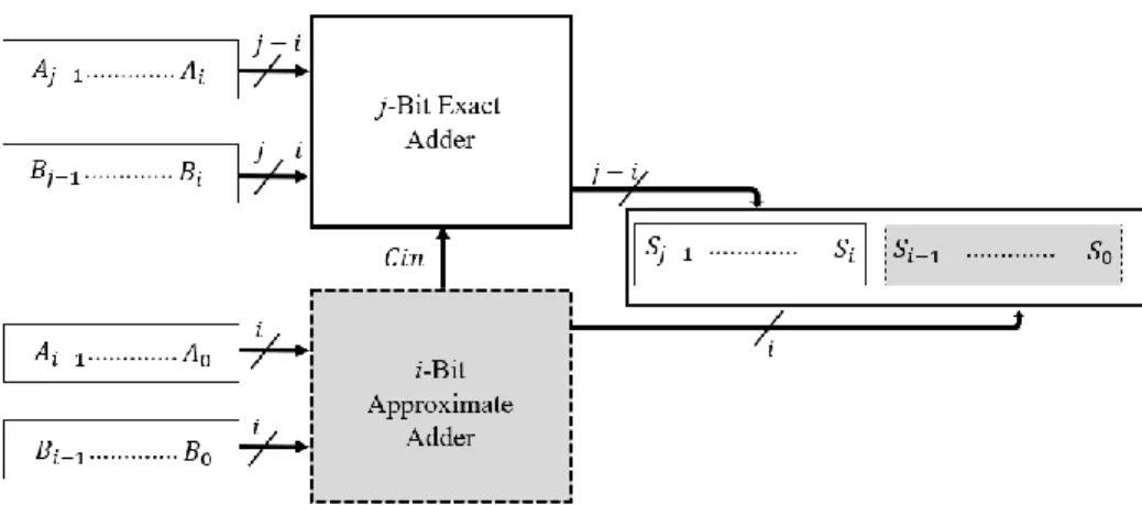
portable electronic system is needed for developing wearable devices. Portable prosthetic systems contain autonomous and networked sensors; each sensor hosts multiple input tactile sensors tightly coupled to the embedded processing unit and power supply [58]. The embedded processing unit locally extracts meaningful information by employing sophisticated methods, e.g., Machine Learning [3], which deals with large dimensions of datasets. Nevertheless, this imposes challenges on the real-time operation and adds a burden regarding power consumption. The demands of the electronic-skin are not satisfied since, as shown by [59], the estimated energy/power is not feasible, i.e., 100 pJ/op, time latency (i.e., around 7 s) is very high and the computational load is of about 1.2 GOPS. Therefore, since the implementation of tactile data decoding algorithms for touch modalities classification requires a high amount of power consumption [10],then our primary goal in the thesis is to implement energy-efficient techniques for embedded machine learning algorithms used for tactile data processing in the e-skin .
1.6 Thesis contributions
The contributions in this thesis, are summarized as follow:
• Two signed approximate multipliers have been designed and implemented. The first one is a rounder multiplier called the “META” multiplier [60] and is based on the Error Tolerant Adder (ETA), which has been implemented instead of the exact adder. While the second one is called “Approximate Baugh-Wooley(BW)” multiplier[61] and is based on the architecture of the exact Baugh-Wooley multiplier, where the approximation is enabled after introducing the approximate adder in the computation of the partial products . The proposed circuits have been
implemented using RTL description in VHDL Hardware Description Language for Virtex-7 xc7vx485tffg1157-1 FPGA device. 10000 inputs have been uniformly selected and simulated in order to compute the accuracy metrics of the designs. The relative error (RE) and the mean relative error (MRE) metrics have been calculated to assess the performance of the approximate multipliers. Results show that approximate-BW is the most efficient design between the approximate multipliers achieving a relevant reduction in power consumption and time delay around 80.4% and 24% respectively with respect to the exact BW multiplier and an improvement of power consumption reduction by 68.1% with respect to other state of the art solutions.
• Implementing approximate arithmetic circuits into the Coordinate Rotational Digital Computer (CORDIC)[62] algorithm and the SVD[63] circuits in order to reduce the power consumption of ML algorithms; since CORDIC and SVD circuits take part of the real-time ML algorithm for tactile data processing. Approximate CORDIC and approximate SVD have been implemented using RTL description in VHDL Hardware Description Language for Virtex-7 xc7vx485tffg1157-1 FPGA device. ETA and LOA have been implemented instead of the entirely precise adder (RCA) into the CORDIC algorithm aiming to study the performance of CORDIC in terms of slices, power and time latency after employing approximate circuits. ETA and LOA in the CORDIC design allow respectively a dynamic power consumption saving up to 13% and 21% with respect to CORDIC-RCA. While for the (SVD) singular Value Decomposition, the Approximate BW multiplier has been implemented in Post rotation and Pre rotation blocks of the SVD after scaling
the approximation in the multiplier by increasing the number of the approximate bits from (8 to 28). Results show that the power consumption of the SVD is reduced by 19% with a negligible accuracy loss.
• Implementing an energy-efficient smart system for tactile sensing based on a RISC-V parallel ultra-low-power platform (PULP). The PULP processor, called Mr. Wolf[64], performs the on-board classification of different touch modalities. This demonstrates the promising use of on-board classification for emerging robot and prosthetic applications. Experimental results demonstrate the effectiveness of the platform on improving energy efficiency and the accuracy of the classification. A memory management strategy has been proposed in order to store 50 trained for each class in L2 memory (512 kB). We evaluated the execution cycles for Mr. Wolf using a single core, 2 cores, and 3 cores to evaluate the benefits of the parallelization. The three SVDs blocks have been executed in parallel on three different cores on the Wolf SoC. A 3.72× speed-up can be achieved after executing SVD (A) ,SVD (B), and SVD(C) blocks on three different cores in parallel. We demonstrated that the algorithm on the proposed platform outperforms ARM Cortex M4F (STM32F40) and by 15 times in terms of energy efficiency, without exceeding the power envelope of a 28mW.
1.7 Organization of the thesis document
The thesis is organized as follows. Chapter 2 describes the architecture of the exact and approximate adders and multipliers presented in state of the art. Then, it presents the architectures of the two new proposed approximate multipliers (META and approximate Baugh-Wooley multipliers). After, an assessment study of the new approximate multipliers
has been done in terms of performance, accuracy, delay, area, and power consumption with respect to state of the art.
Chapter 3 assesses the impact of the new approximate multipliers designs as well as some of the most relevant state of the art approximate multipliers on tactile digital signal processing. The quality is measured in terms of different metrics, mainly: SNR degradation, power consumption, and time delay. On the other hand, approximate computing techniques have been applied on the machine learning algorithm employed for the tactile data processing; by implementing approximate adders and multipliers into the Coordinate Rotational Digital Circuits (CORDIC) and the Singular Value Decomposition (SVD) algorithms which take a significant part of the real-time ML algorithm.
Chapter 4 presents the machine learning algorithms employed for tensorial tactile data processing. Moreover, it discusses the reasons behind following the mentioned approach. Then, the SVM based tensor kernel algorithm is implemented in C language in order to validate the effectiveness of the algorithm when classifying images (as a case study) and touch modalities.
Chapter 5 describes the hardware implementation of the SVM based tensor kernel approach on a novel computing platform embedding a Parallel Ultra Low Power processor (PULP), called “Mr. Wolf” for the aim to reach an embedded low power implementation for wearable devices. The classification based on Support Vector Machine (SVM) runs directly on PULP classifying two touch modalities (finger sliding and washer rolling) outperforming ARM Cortex M4 in terms of power consumption and energy efficiency.
CHAPTER 2.
LOW POWER APPROXIMATE
ARITHMETIC CIRCUITS.
2.1 Introduction
Energy-efficiency has become a paramount concern in designing computing systems. The ever-increasing demand for higher computing power represents a driving force toward ultra-low power design strategies. Low power consumption is the most critical design goal for a wide range of electronic systems, including smart self-powered sensing systems for such application domains as the Internet of Things (IoT), Wearable Devices and Robotics. To improve energy efficiency, at different layers of the system stack, researchers have developed different optimizations methods.
In recent years, several techniques at the circuit and system level have been proposed to address this issue. One of these techniques is “approximate computing,” which turned out to be a practical approach providing a tradeoff between accuracy and power saving to improve performance and energy efficiency [1],[2]. Approximate results are usually acceptable for many applications requiring tactile data processing [3], [4] image processing [5], and data mining [6]. Thus, it is highly recommended to take advantage of energy reduction with minimal variation in performance [7]. Recently, approximations have been used in computing units of embedded systems, especially graphics processing units (GPUs) and field-programmable arrays (FPGAs) [65]. Computing units, e.g., embedded digital signal processing (DSP) systems, are considered critical components of modern electronic embedded devices [55]. Among arithmetic DSP operations, multiplication is considered as
a complex block consuming a high amount of power with significant time latency when compared to other operations. Decreasing the complexity of multiplication blocks may reduce the power consumption of DSP systems. In this perspective, the proposed work employs approximate computing techniques for the arithmetic units, i.e., adders and multipliers for energy-efficient data processing units. In this chapter, we present an overview of entirely precise and approximate adders and multipliers circuits. Then we describe the architectures of the two new proposed approximate multipliers (META and approximate Baugh-Wooley multiplier). After, an assessment study of the proposed approximate multipliers has been done in terms of performance, accuracy, delay, area, and power consumption with respect to state of the art. Therefore, the main goal is to implement efficient hardware architectures of approximate multipliers providing low power consumption. The results presented in this chapter were published in [60],[61],[130].
2.2 Background on Adders and Multipliers
This section presents the architecture of some relevant exact arithmetic circuits in state of the art.
2.2.1 Representation of signed integers
In this section, we will discuss the representation of signed integers (positive and negative). Usually, two representations are presented such as: the sign and magnitude representation and the true-and-complement representation.
2.2.1.1 Sign-and-Magnitude (SM) Representation
In the SM system, the signed integer 𝑥 is represented by a pair of (𝑎1, 𝑎𝑚), where 𝑎1is the sign and 𝑎𝑚 is the magnitude. The values of two sign (+, −) are usually represented by a binary variable; where the integer 1 corresponds to – and 0 corresponds to +. When representing the positive integers, the magnitude could be represented in any system. In case of conventional radix-r system, the range of signed integers is presented as equation below:
0 ≤ 𝑎𝑚 ≤ 𝑟𝑛− 1 (2.1)
2.2.1.2 True-and -Complement (TC) Representation
No separation is applied between the representation of the sign and the magnitude in the TC system. But in this system, all the signed integer is represented by a positive integer. Therefore, the signed integer 𝑥 is represented by positive integer called 𝑎𝑅which is expressed as below:
𝑎𝑅 = 𝑎 𝑚𝑜𝑑 𝐶 (2.2)
Where the positive integer 𝐶 is called the complementation constant. For max|𝑎| < 𝐶, the following system could be derived:
𝑎𝑅 = { 𝑎 if 𝑎 ≥ 0
𝐶 − |𝑎| = 𝐶 + 𝑎 if 𝑎 ≥ 0 (2.3)
However, the region for 𝑎 > 0 should not overlap with the region for 𝑎 < 0. This requires that:
max|𝑎| <𝐶
2 (2.4)
In this case, the following system could be derived:
𝑎 = {𝑎𝑅,,……..,,,,,,,,,,, 𝑎𝑅 < 𝐶/2 𝑎𝑅 − 𝐶 𝑎𝑅 ≥ 0
(2.5)
When 𝑎𝑅 = 𝐶/2 is representable, it is usually assigned to 𝑎 = −𝐶/2, making the
representation asymmetrical. So, the true forms indication corresponds to the positive integer’s representation, while the complement forms correspond to negative integer’s representation.
2.2.2 Basic Adders
2.2.2.1 Ripple-Carry Adder
Ripple-Carry Adder (RCA) [66] is a well-known circuit used to compute the addition of two binary numbers in many arithmetic circuits. RCA adds sequentially the bits having the same significance and the carry-bit from the previous stage using a full adder (FA), then propagates the carry-bit to the following stage, as shown in Fig. 2.1. This adder could be employed for adding both unsigned and two’s complement numbers. However, the main drawback of RCA is that the worse-case delay is intended to be proportional to the word length. Moreover, since the full adder cells are supposed to wait for the correct carry input,
thus many glitches will be produced from the RCA. Nevertheless, this drawback could be improved if the delay of the carry bit is smaller than that of the sum bit.
2.2.2.2 Carry-Chain Adder
Fig.2.2. shows the structure of an n-digit adder having a separate carry calculation. The generate and the propagate functions are calculated through the G-P (generate-propagate) cell based on the following equations:
𝑔(𝑖) = { 1 if 𝑎(𝑖) + 𝑏(𝑖) > 𝐵 − 1
0 otherwise (2.6)
𝑝(𝑖) = { 1 if 𝑎(𝑖) + 𝑏(𝑖) = 𝐵 − 1
0 otherwise (2.7)
Where 𝑎(𝑖) and 𝑏(𝑖) are the inputs signals, and 𝐵 represents the Base.
The next carry is computed through the C.C. (carry-chain) cell as follow:
𝐶(𝑖 + 1) = { 𝐶(𝑖) if 𝑔(𝑖) = 1
𝑔(𝑖) otherwise (2.8)
Then a carry is generated from 𝑔(𝑖) and the carry is propagated from level i-1 by
𝑝(𝑖).Then the sum will be generated through the 𝑚𝑜𝑑 𝐵 sum cell as follow:
𝑆(𝑖) = (𝑎(𝑖) + 𝑏(𝑖) + 𝐶(𝑖))𝑚𝑜𝑑 𝐵 (2.9)
2.2.2.3 Carry-Lookahead Adder (CLA)
The main concept of this adder is to compute simultaneously several carries. In the extreme, the computation of the carries is done at the same time. Let’s consider that 𝑎(𝑖)and
𝑏(𝑖)the integers represented by the bit-vector from bit 0 to bit 𝑖 as follow:
𝑎(𝑖)= ∑ 𝑎 𝑣2𝑣 𝑖
𝑣=0 (2.10)
and similarly, for 𝑏(𝑖), the carry is computed as follow:
𝑐𝑖 = 1 if (𝑎(𝑖−1)+ 𝑏(𝑖−1)+ 𝑐0 ≥2𝑖 (2.11)
Then, a switching function of 2𝑖 + 1 variables will be resulted. This function could be implemented by a two-level network such as: 𝑁𝐴𝑁𝐷 − 𝑁𝐴𝑁𝐷.In case of large i, this implementation is complex due to the large number of gates and inputs. Therefore, the input vector in the CLA is divided into two groups, where the carries are computed simultaneously.
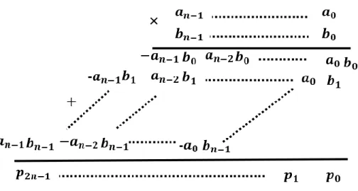
Multiplication of two numbers is usually executed by following the two main steps:
a) Generation of partial products where the partial product is the result of multiplication of the multiplicand with a bit of the multiplier.
b) Partial products accumulation
In this section, we will discuss some techniques to simplify the summation of the partial product, and we will describe the architecture of some exact multipliers.
2.2.3.1 Partial Product Generation
For unsigned number format, the multiplication is done based on the following equation:
𝑃 = 𝐴𝐵 = ∑𝑛𝑖=1𝑎𝑖2−𝑖∑ 𝑏 𝑗 𝑛
𝑗=1 2−𝑗 (2.12)
A partial product array is generated, as shown in Fig. 2.3., where partial products are applied through AND gates. In the case of 2’s complement representation as shown in
Fig.2.4, the equation is similar to (2.10) except that some bits will have a negative weight. The equation is shown below:
𝑃 = 𝐴𝐵 = 𝑎0𝑏0− 𝑎0∑𝑗=1𝑛 𝑏𝑗2−𝑗− 𝑏0∑𝑖=1𝑛 𝑎𝑖2−𝑖+ ∑𝑛𝑖=1∑𝑛𝑗=1𝑎𝑖𝑏𝑗2−𝑖−𝑗 (2.13)
2.2.3.2 DADDA Multipliers
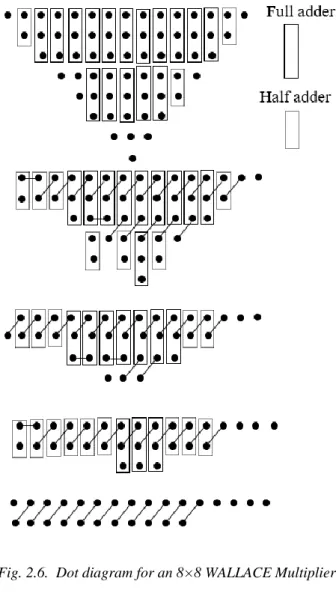
DADDA multipliers [67] are considered as the remake design of the parallel multipliers presented by Wallace in 1964 [68]. As shown in Fig. 2.5, the multiplier is composed of three stages, wherein the first stage a partial product by 𝑁2AND gates are executed. In the
second stage, the height of the partial product matrix is reduced to two, which employs different parallel (𝑚, 𝑛) counters. The parallel counter in DADDA multiplier has m inputs providing n outputs. During the compression phase, DADDA multiplier employs at least
(3,2) and (2,2) counters at each level, where a (3,2) and (2,2) counters represent respectively a full adder and a half adder. In Fig.2.5, the outputs of the (3,2) counter are
represented by a diagonal line joining the two squares, while the crossed diagonal line joining the other two squares are the outputs of the (2,2) counter. In order to produce a 16-bit product multiplier, different components are required such as: 64 AND gates, 35
(3,2) counters, 7 (2,2) counters and a 14-bit carry propagation adder. During the compression stage, DADDA multipliers require less counters than Wallace multipliers. Lastly, the final stage of the multiplier uses a carry propagation adder in order to generate the final product.
2.2.3.3 WALLACE Multipliers
Similarly to DADDA multiplier, the partial products in WALLACE [68] multiplier are produced through 𝑁2 AND gates as shown in Fig.2.6. Then a set of three rows are grouped together containing N rows of partial products. While each row which is not included in the set of the three rows is transferred to the next phase without applying any change. Then
(3,2) and (2,2) counters are applied to columns containing three bits and columns containing two bits, respectively. Nevertheless, each column that contains a single bit will
be transferred to the next level without any modification. In WALLACE multipliers, a carry propagating adder is employed for the execution of the final addition whose sum is the product of the final multiplication. During the reduction phase, the WALLACE multiplier has approximately the same numbers of full adders, similarly to the DADDA multiplier. Then a shorter final carry propagating adder is generated after adding half adders to the previous phase. The components required to produce a 16-bit product DADDA multiplier are as follow: 64 AND gates, 1 OR gate, 38 (3,2) counters, 15 (2,2) counters, and a 10-bit carry propagating adder.
2.2.3.4 Baugh-Wooley Multiplier
Baugh-Wooley [69] is a well-known algorithm used to compute the multiplication in many digital signal processing units. It is a signed array multiplier considered in our case as an exact reference multiplier to be compared with the proposed approximate ones [70],
[69]. Baugh-Wooley is designed to compute the multiplication of both signed and unsigned operands using 2’s complement number system. During direct multiplication of two 2's complement numbers, the partial products obtained will be signed numbers. Hence sign extension is needed for these partial products to the final product's width to get the accurate answer. This multiplier is very easy to implement since it has a regular architecture as shown in fig.2.7. Moreover, Baugh Wooley multiplication table can be implemented using different full adders such as: carry save array, ripple carry adder or carry select adder. In case of 4 × 4 multiplication, 3 rows of adders and a final stage adder are needed for the computation, where the partial products are obtained using AND and NAND gates.
2.3 Background on approximate adders and multipliers
In this section, some significant approximate arithmetic circuits (adders and multipliers) are described and presented.
2.3.1 Approximate Adders
In [71], an approximate adder based on the dynamic segmentation with the error compensation technique (DSEC) is proposed. The n-bit adder is divided into smaller sub-adders operating in parallel with fixed carry inputs. This technique reduces 30% power consumption. Authors in [72] described an n-bit Carry Skip Adder (CSA) which is divided into [n/k] blocks. Each block is made of a sub-carry generator and a sub-adder. The power consumption is reduced by 43% when compared to exact adders.
In contrast to SCSA, the speculative carry adder (CSPA) presented in [73] is composed of one sum generator, two internal carry generators, and one carry predictor for each block. The energy efficiency and time delay are improved respectively by 19.03%
and 26.59% with respect to the existing speculative carry-select adder. In [74], the Gracefully-Degrading accuracy-configurable adder (GDA) is presented. Through the control signals, the accuracy of GDA is configured by selecting the approximate of exact carry-in for each sub-adder through a multiplexer. This advanced design achieves a better quality when compared to existing techniques. The consistent Carry Approximate Adder (CCA) based on SCSA, is proposed in [75]: the carry prediction depends on the least significant bit (LSBs) and the MSBs. The time delay and the area are similar to SCSA. Authors in [55] proposed the Lower-Part-OR Adder (LOA), which is based on processing the least significant bits using OR gates. In [76], Approximate Mirror Adders (AMAs) are proposed. The AMAs are implemented in the LSBs of a multiple-bit adder achieving a reduction in power consumption by up to 69% when compared to accurate adders. Authors in [77] proposed three approximate adders (AXAs) based on XOR and XNOR logic gates consuming less power than the exact XOR/XNOR-based adder.
2.3.2 Approximate Multipliers
Efficient implementations of approximate multipliers based on different approaches have been recently reported in the literature. Kulkarni et al. [78] proposed an approximate 2×2 multiplier cell, which is employed as a basic block for multiplier architectures having a larger size. An average of 31.8% improves energy efficiency to 45.4% with respect to exact multipliers. Authors in [79] have presented an accuracy-configurable multiplier architecture (ACMA) for error-resilient designs. This architecture is based on a technique called carry-in prediction, employing an efficient precomputation logic, which reduces the latency to around 50% when compared to an accurate multiplier. [80] presented an Approximate Wallace Tree Multiplier (AWTM), which employs a carry-in prediction
reducing the power consumption by 42% with respect to the Wallace tree multiplier (WTM). The Partial Product Perforation technique (PPP) presented in [81] is based on neglecting a specific number of partial products, reducing the power consumption and time delay around 50% and 35%, respectively, when compared to an exact design. [82] proposed an approximate (4:2) counter for an approximate 4-bit Wallace multiplier. This inexact multiplier is employed in order to build more massive multipliers having error detection and correction circuits. The power consumption is reduced by 10.7% when compared to the Wallace tree multiplier. Two approximate 4:2 compressors have been proposed in [83], providing efficient reductions in power consumption, hardware resources, and delay with respect to exact designs. Authors in [84] proposed a static segment multiplier (SSM), which takes m segment bits from n-bit operand based on leading 1 bit of the operands. Then, instead of n × n multiplication, the m × m multiplication is executed, where (m<n). It consumes 58% less energy when compared to a precise multiplier with an average computational error of around 1%. In [70], a new multiplier is proposed, which connects the most significant bit (MSB) to the least significant (LSB), generating an error value of 1. Sekanina in [85] provided an open-source library of approximate adders and multipliers called EvoApprox8b library. Authors in [70] have proposed an efficient multiplier based on the rounding approach. Speed and power consumption have been reduced after omitting the computational part of the multiplication.
2.4 Low Power Approximate Adders and Multipliers
In this section, the relevant state of the art approximate arithmetic circuits, i.e., approximate adders and multipliers, are reported, and novel approximate circuits are proposed.
2.4.1 Approximate Adders Circuits
The full adders consume a high amount of power such as the CLA while other are slow(i.e.: RCA). Thus, approximate adders have been proposed in the literature [77], [55],[86], trading the accuracy for a reduction in power, time delay, and hardware resources. Fig.2.8 represents the general circuit architecture for approximate adder circuits. It divides the addition operation into two blocks: 1) Exact and 2) Approximate. The exact operation deals with the most significant bits of the addition while the approximate one oversees the least significant bits. The error is decreased by using a carry-in signal from approximate to the exact block. The architecture provides the possibility to scale the number of bits in the exact and inexact parts. Consequently, the effect of varying the inexactness represented by the scalability of the number of bits with respect to accuracy could be analyzed. Based on the general architecture, the following subsections introduce the proposed adder with some relevant circuit from state of the art.
2.4.1.1 Approximate XNOR-based Adder (AXA)
Fig.2.9 (a) shows the functionally equivalent remakes design of the original approximate XNOR-based Adder (AXA) [77]. The signal is generated after applying an XNOR logic operation for the two input bits A and B. The sum signal is correct for half of the possible input combinations, Cout is exact for all the input combinations, and it is generated
according to the following equation:
𝑆 = (𝐴 𝐴𝑁𝐷 𝐵) 𝑂𝑅 (𝐴 𝑋𝑂𝑅 𝐵) 𝐴𝑁𝐷 𝐶𝑖𝑛 (2.14) (a) (b) (c) (d) (e) (f)
Fig.3 Approximate adder circuits
Fig. 2.9. Approximate adder circuits: (a) AXA, (b) Lower-Part-Or-Adder, (c) Approximate NAND-carry out bit, (d) Approximate AND-carry out bit, (e) Input Pre-Processing, (f) AFA adder
2.4.1.2 Lower-Part-OR-Adder
In the approximate part of the lower part OR adder (LOA) [55] presented by Fig.2.9 (b), OR gates are applied to the respective A and B input bits. An AND gate is applied to the most significant bits of both A and B generating the carry out (Cout) signal. In order to
decrease the inaccuracy, Cout is connected to the upper part of the adder (exact operation)
when the most significant bits are equal to one.
2.4.1.3 Approximate NAND-carry out bit
As shown in Fig.2.9 (c) [86], the approximation is applied to the carry-out signal by omitting the two min-terns in the regular expression of Cout as given by (2.14). Then the approximation is expressed by executing a NAND logic operation between A and B. The sum signal is generated at the end by applying the following operation:
𝑆 = (𝐴 𝑋𝑁𝑂𝑅 𝐵)𝑋𝑂𝑅 𝐶𝑖𝑛 (2.15)
2.4.1.4 Approximate AND-carry out bit
Similar to the approximate NAND-carry out bit [86], this adder adopts an AND gate operation for both inputs A and B generating the approximate Cout signal, as shown in
Fig.2.9 (d). The signal sum performs the following operation:
𝑆 = (𝐴 𝑋𝑂𝑅 𝐵) 𝑋𝑂𝑅 𝐶𝑖𝑛 (2.16)
2.4.1.5 Input Pre-Processing
The Input Pre-Processing approximate adder is presented in Fig. 2.9 (e). It is based on interchanging the bits having the same weights in different addends. The original adder has
been proposed in [87]; it generates two signals: sum and error. However, only the sum signal is taken into consideration here. The sum signal resulted is based on the following logic operation:
𝑆 = (𝐴𝑖 𝑋𝑂𝑅 𝐵𝑖) 𝑂𝑅 (𝐴𝑖−1 𝐴𝑁𝐷 𝐵𝑖−1) (2.17)
2.4.1.6 New Approximate Adder (AFA)
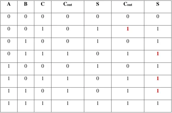
The truth table of AFA adder is illustrated in Table 2.1. Moreover, the equations of the approximate carry bit and the approximate sum bit are shown below:
𝐶𝑜𝑢𝑡 = 𝐶𝑖𝑛+ 𝐴. 𝐵 (2.18)
𝑆 = 𝐶𝑜𝑢𝑡 + (𝐴 ⊕ B) (2.19)
Table 2.1. Truth table for AFA Adder
Inputs Exact Outputs Approximate Outputs
A B C Cout S Cout S 0 0 0 0 0 0 0 0 0 1 0 1 1 1 0 1 0 0 1 0 1 0 1 1 1 0 1 1 1 0 0 0 1 0 1 1 0 1 1 0 1 1 1 1 0 1 0 1 1 1 1 1 1 1 1 1