Available online:
https://edupediapublications.org/journals/index.php/IJR/
P a g e
| 637
Design And Implementation Of Dual Voltage Source Inverter Using
Fractional Order Pid Controller
E.Rajendra
1; N.Rajeshkumar Gowd
2; P. Shashavali
31
P.G Student, S.K.U College of Engg. & Tech., S.K. University, Ananathapuramu-515 003.
2& 3
Lecturer in EEE Department, S.K.U College of Engg. & Tech., S.K. University, Ananthapuramu-515 003.
Abstract
: This paper presents a dual voltage sourceinverter (DVSI) scheme with Fractional Order PID controller (FOPID) to enhance the power quality and reliability of the microgrid system. The proposed DVSI scheme is comprised of two inverters, which enables the microgrid to exchange power generated by the distributed energy resources (DERs) and also to compensate the local unbalanced and nonlinear load. The control algorithms are developed based on instantaneous symmetrical component theory (ISCT) with FOPID Controller to operate DVSI in grid sharing and grid injecting modes. The proposed scheme has increased reliability, lower bandwidth requirement of the main inverter, lower cost due to reduction in filter size, and better utilization of microgrid power while using reduced dc-link voltage rating for the main inverter. These features make the DVSI scheme a promising option for microgrid supplying sensitive loads. The topology and control algorithm are validated through extensive simulation and experimental results.
Key words:
Grid connected inverter, reactive power compensation, Fractional Order PID Controller (FOPID) instantaneous symmetrical component theory (ISCT), microgrid, power quality.I INTRODUCTION
Technological progress and environmental
concernsdrive the power system to a paradigm shift with morerenewable energy sources integrated to the network by meansof distributed generation (DG). These DG units with coordinatedcontrol of local generation and storage facilities form amicrogrid [1]. In a microgrid, power from different renewableenergy sources such as fuel cells, photovoltaic (PV) systems,and wind energy systems are interfaced to grid and loads usingpower electronic converters. A grid interactive inverter plays animportant role in exchanging power from the microgrid to thegrid and the connected load [2],[3]. This microgrid invertercan either work in a grid sharing mode while supplying a partof local load or in grid injecting mode, by injecting power tothe main grid.
Maintaining power quality is another important aspect whichhas to be addressed while the microgrid system is connected tothe main grid. The proliferation of power electronics devicesand electrical loads with unbalanced nonlinear currents hasdegraded the power quality in the power distribution network.Moreover, if there is a considerable amount of feeder impedance in the distribution systems, the propagation of theseharmonic
currents distorts the voltage at the point of
commoncoupling (PCC). At the same instant, industry automation hasreached to a very high level of sophistication, where plantslike automobile manufacturing units, chemical factories, andsemiconductor industries require clean power. For these applications,it is essential to compensate nonlinear and unbalancedload currents [4].
Load compensation and power injection using grid interactiveinverters in microgrid have been presented in the literature [5],[6]. A single inverter system with power quality enhancement [7] . The main focus of this work is torealize dual functionalities in an inverter that would provide theactive power injection from a solar PV system and also works asan active power filter, compensating unbalances and the reactivepower required by other loads connected to the system.In[8] a voltage regulation and power flow control schemefor a wind energy system (WES) is proposed. A distributionstatic compensator (DSTATCOM) is utilized for voltageregulation and also for active power injection. The controlscheme maintains the power balance at the grid terminal duringthe wind
variations using sliding mode control. A
multifunctionalpower electronic converter for the DG power system [9]. This scheme has the capability to inject powergenerated by WES and also to perform as a harmonic compensator.
Available online:
https://edupediapublications.org/journals/index.php/IJR/
P a g e
| 638
achieving the secondobjective is decided by the available instantaneous microgridreal power [10]. Considering the case of a grid-connected PVinverter, the available capacity of the inverter to supply the reactivepower becomes less during the maximum solar insolationperiods [11]. At the same instant, the reactive power to regulatethe PCC voltage is very much needed during this period [12]. It indicates that providing multifunctional tiesin a singleinverter degrades either the real power injection or the loadcompensation capabilities.
The contents of this paper are as follows. First, the configuration of the system with dual voltage source inverter (DVSI) is described. The dynamic equations for the load, the VSI ac side system, and the VSI dc side system are then derived. When the dynamic equations for the system are linearized around a nominal loading condition, we can proceed to design a fixed-gain PI controller for the DVSI using the linearized state equations. Then, a Fractional Order PID controller for the DVSI is designed. Finally, MATLAB Simulation results are presented to demonstrate the effectiveness of the proposed FOPID controller for the STATCOM.
II DUAL VOLTAGE SOURCE INVERTER
A. System Topology
The proposed DVSI topology is shown in Fig. 1. It consistsof a neutral point clamped (NPC) inverter to realize AVSIand a three-leg inverter for MVSI [15]. These are connectedto grid at the PCC and supplying a nonlinear and unbalancedload. The function of the AVSI is to compensate the reactive,harmonics, and unbalance components in load currents. Here,load currents in three phases are represented by ila, ilb, and ilc,respectively. Also,
ig(abc), iμgm(abc), and iμgx(abc) show gridcurrents, MVSI
currents, and AVSI currents in three phases,respectively. The dc link of the AVSI utilizes a split capacitortopology, with two capacitors C1 and C2. The MVSI deliversthe available power at distributed energy resource (DER)to grid.
Fig.1. Topology of proposed DVSI scheme.
The DER can be a dc source or an ac source with rectifier coupled to dc link. Usually, renewable energy sources like fuel cell and PV generate power at variable low dc voltage, while the variable speed wind turbines generate power at variable ac voltage. Therefore, the power generated from these sources use a power conditioning stage before it is connected to the input of MVSI. In this study, DER is being represented as a dc source. An inductor filter is used to eliminate the high-frequency switching components generated due to the switching of power electronic switches in the inverters [16]. The system considered in this study is assumed to have some amount of feeder resistance Rgand inductance Lg. Due to the presence of this feeder impedance, PCC voltage is affected with harmonics. Section III describes the extraction of fundamental positive sequence of PCC voltages and control strategy for the reference current generation of two inverters in DVSI scheme using FOPID controller.
B. Design of DVSI Parameters
1) AVSI: The important parameters of AVSI like dc-linkvoltage (Vdc), dc storage capacitors (C1 and C2),
interfacinginductance (Lfx), and hysteresis band (±hx) are selected basedon the design method of split capacitor DSTATCOM topology. The dc-link voltage across each capacitor is taken as1.6 times the peak of phase voltage. The total dc-link voltagereference (Vdcref) is found to be
1040 V.
Values of dc capacitors of AVSI are chosen based on thechange in dc-link voltage during transients. Let total load ratingis S kVA. In the worst case, the load power may vary fromminimum to maximum, i.e., from 0 to S
kVA. AVSI needsto exchange real power during transient to maintain the loadpower demand. This transfer of real power during the transientwill result in deviation of capacitor voltage from its referencevalue. Assume that the voltage controller takes n cycles, i.e.,nTseconds to act, where T is the system time period. Hence,maximum energy exchange by AVSI during transient will benST. This energy will be equal to change in the capacitorstored energy. Therefore
… (1)
whereVdcr and Vdc1 are the reference dc voltage and
maximumpermissible dc voltage across C1 during transient,
respectively.Here, S =5 kVA, Vdcr = 520 V, Vdc1 = 0.8 *Vdcr
or 1.2 *Vdcr,n = 1, and T = 0.02 s. Substituting these values
in (1), the dclinkcapacitance (C1) is calculated to be 2000
Available online:
https://edupediapublications.org/journals/index.php/IJR/
P a g e
| 639
The interfacing inductance is given by
… (2)
Assuming a maximum switching frequency (fmax) of 10
kHzand hysteresis band (hx) as 5%of load current (0.5 A), the valueof Lfxis calculated to be 26 mH.
2) MVSI: The MVSI uses a three-leg inverter topology. Itsdc-link voltage is obtained as 1.15 *Vml, where Vmlis the peakvalue of line voltage. This is calculated to be 648 V. Also,MVSIsupplies a balanced sinusoidal current at unity power factor. So,zero sequence switching harmonics will be absent in the outputcurrent of MVSI. This reduces the filter requirement for MVSIas compared to AVSI. In this analysis, a filter inductance(Lfm) of 5mH is used.
C. Advantages of the DVSI Scheme
The various advantages of the proposed DVSI scheme over asingle inverter scheme with multifunctional capabilities [7]-[9] are discussed here as follows:
i. Increased Reliability: DVSI scheme has increased reliability,due to the reduction in failure rate of components andthe decrease in system down time cost. In this scheme, thetotal load current is shared between AVSI and MVSI and hencereduces the failure rate of inverter switches. Moreover, if oneinverter fails, the other can continue its operation. This reducesthe lost energy and hence the down time cost. The reduction insystem down time cost improves the reliability.
ii. Reduction in Filter Size: In DVSI scheme, the currentsupplied by each inverter is reduced and hence the current ratingof individual filter inductor reduces. This reduction in currentrating reduces the filter size. Also, in this scheme, hysteresiscurrent control is used to track the inverter reference currents.As given in (2), the
filter inductance is decided by the
inverterswitching frequency. Since the lower current rated semiconductordevice can be switched at higher switching frequency,the inductance of the filter can be lowered. This decrease ininductance further reduces the filter size.
iii. Improved Flexibility: Both the inverters are fed fromseparate dc links which allow them to operate independently,thus increasing the flexibility of the system. For instance, if thedc link of the main inverter is disconnected from
the system, theload compensation capability of the auxiliary inverter can stillbe utilized. iv. Better Utilization of Microgrid Power: DVSI
schemehelps to utilize full capacity of MVSI to transfer the entirepower generated by DG units as real power to ac bus, asthere is AVSI for harmonic and reactive power compensation.This increases the active power injection capability of DGs inmicrogrid.
v. Reduced DC-Link Voltage Rating: Since, MVSI is notdelivering zero sequence load current components, a singlecapacitor three-leg VSI
topology can be used. Therefore, the
dclinkvoltage rating of MVSI is reduced approximately by 38%,as compared to a single inverter system with split capacitor VSItopology.
III. CONTROL STRATEGY FOR DVSI SCHEME
A. Fundamental Voltage Extraction
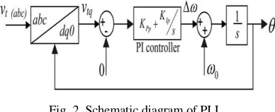
The control algorithm for reference current generation usingISCT requires balanced sinusoidal PCC voltages. Because ofthe presence of feeder impedance, PCC voltages are distorted.Therefore, the fundamental positive sequence components ofthe PCC voltages are extracted for the reference current generation.To convert the distorted PCC voltages to balancedsinusoidal voltages,
Fig. 2. Schematic diagram of PLL.
dq0 transformation is used. The PCC voltagesin natural
reference frame (vta, vtb, and vtc) are firsttransformed into
dq0 reference frame as given by
where …(3)
Available online:
https://edupediapublications.org/journals/index.php/IJR/
P a g e
| 640
The frequency deviation Δωis then added to the reference frequencyω0 and finally given to the integrator to
get θ. It can beproved that, when, θ = ω0t and by using the
Park’s transformationmatrix (C), q-axis voltage in dq0
frame becomes zero andhence the PLL will be locked to the reference frequency (ω0).As PCC voltages are distorted, the
transformed voltages in dq0frame (vtdand vtq) contain
average and oscillating componentsof voltages. These can be represented as
vtd= vtq+ _vtd, vtq= vtq+ _vtq ....(4)
wherevtdand vtqrepresent the average components of
vtdandvtq, respectively. The terms _vtdand _vtqindicate the oscillatingcomponents of vtdand vtq, respectively. Now the fundamentalpositive sequence of PCC voltages in natural reference framecan be obtained with the help of inverse dq0
transformation asgiven by
…(5)
These voltages v+ta1, v+tb1, and v+tc1 are used in the
referencecurrent generation algorithms, so as to draw balanced sinusoidalcurrents from the grid.
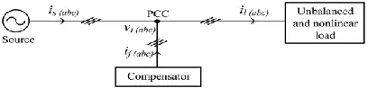
B. Instantaneous Symmetrical Component Theory
ISCT was developed primarily for unbalanced and nonlinearload compensations by active power filters. The system topologyshown in Fig. 3 is used for realizing the reference currentfor the compensator. The ISCT for load compensation isderived based on the following three conditions.
Fig 3. Schematic diagram of an unbalanced and nonlinear load compensation scheme.
1) The source neutral current must be zero. Therefore
isa+ isb+ isc= 0.
…
(6)
2) The phase angle between the fundamental
positivesequence voltage (v+ta1) and source current (isa) is φ
∠v+ta1 = ∠isa+ φ…
(7)
3) The average real power of the load (Pl) should be suppliedby the source
v+ta1isa+ v+tb1isb+ v+tc1isc= Pl.…
(8)
Solving the above three equations, the reference source currentscan be obtained as
… (9)
whereβ = tan φ/√3. The termφ is the desired phase angle betweenthe fundamental positive sequence of PCC voltage and sourcecurrent. To achieve unity power factor for source current, substituteβ = 0in (9). Thus, the reference source currents for threephases are given by
… (10)
wherei*sa, i*sb, and i*scare fundamental positive sequence ofload currents drawn from the source, when it is supplying anaverage load power Pl. The power Pl can be computed using amoving average filter with a window of one-cycle data pointsas given below
… … (11)
wheret1 is any arbitrary time instant. Finally, the
referencecurrents for the compensator can be generated as follows:
... (12)
Equation (12) can be used to generate the reference filtercurrents using ISCT, when the entire load active power, Pl issupplied by the source and load compensation is performedby a single inverter. A modification in the control algorithmis required, when it is used for DVSI scheme. The followingsection discusses the formulation of control algorithm forDVSI scheme. The source currents, is(abc) and filter currentsif(abc) will be
equivalently represented as grid currents ig(abc)and AVSI
currentsiμgx(abc), respectively, in further sections.
C. Control Strategy of DVSI
Control strategy of DVSI is developed in such a way thatgrid and MVSI together share the active load power, and AVSIsupplies rest of the power components demanded by the load.
1) Reference Current Generation for Auxiliary Inverter:
Available online:
https://edupediapublications.org/journals/index.php/IJR/
P a g e
| 641
inverter. DC-link voltagevariation occurs in auxiliary inverter due to its switching andohmic losses. These losses termed as Ploss should also be suppliedby the grid. An
expression for Ploss is derived on thecondition that average
dc capacitor current is zero to maintaina constant capacitor voltage [14]. The deviation of averagecapacitor current from zero will reflect as a change in capacitorvoltage from a steady state value. A PI controller is used togenerate Ploss
term as given by
... (13)
whereevdc = Vdcref− vdc, vdc represents the actual
voltagesensed and updated once in a cycle. In the above equation, KPvand KIvrepresent the proportional and integral gains of dc-linkPI controller, respectively. Here, the dc-link voltage PIcontroller gains are selected so as to ensure stability and betterdynamic response during load change
…(14)
2) Reference Current Generation for Main Inverter:
MVSI supplies balanced sinusoidal currents based on the availablerenewable power at DER. If MVSI losses are neglected,the power injected to grid will be equal to that available at DER(Pμg).The following equation, which is derived from ISCT canbe used to generate MVSI reference currents for three phases(a, b, andc)
… (15)
wherePμgis the available power at the dc link of MVSI.The reference currents obtained from (14) to (15) are trackedby using hysteresis band current controller (HBCC). HBCCschemes are based on a feedback loop, usually with a two-level comparator.
This controller has the advantage of peak current limiting capacity, good dynamic response, and simplicity in implementation [13]. A hysteresis controller is a high-gain proportional controller. This controller adds certain phase lag in the operation based on the hysteresis band and will not make the system unstable. Also, the proposed DVSI scheme uses a first-order inductor filter which retains the closed-loop system stability. The entire control strategy is
schematically represented in Fig. 4. Applying Kirchhoff’s current law (KCL) at the PCC in Fig. 4
iμgx j= il j − (ig j + iμgmj), for j = a, b, c. …(16)
Fig. 4. Schematic diagram showing the control strategy of proposed DVSI scheme.
By using (14) and (16), an expression for reference grid currentin phase-a (i*ga) can be obtained as
… (17)
It can be observed that, if the quantity (Pl+ Ploss)
is greaterthan Pμg, the term[(Pl+ Ploss) − Pμg] will be a
positive quantity,and i*gawill be in phase with v+ta1. This
operation can becalled as the grid supporting or grid sharing mode, as the totalload power demand is shared between the main inverter andthe grid. The term, Ploss is
usually very small compared to Pl.
On the other hand, if (Pl+ Ploss) is less than Pμg,
then [(Pl+Ploss) − Pμg] will be a negative quantity, and
hence i*gawill bein phase opposition with v+ta1. This mode
of operation is calledthe grid injecting mode, as the excess power is injected to grid.
3)
Fractional Order PID Controller
A PID controller is a generic control loop feedback mechanism widely used in industrial control systems. The PID controller attempts to correct the error between a measured process variable and a desired set point by calculating and then outputting a corrective action that can adjust the process accordingly. An integer order PID controller has the following transfer function:
… (18)
The PID controller calculation (algorithm) involves three separate parameters; the Proportional (K p),
the Integral ( Ki ) and Derivative ( Kd ) time-constants. The
Available online:
https://edupediapublications.org/journals/index.php/IJR/
P a g e
| 642
error, the Integral determines the reaction based on the sum of recent errors and the derivative determines the reaction to the rate at which the error has been changing. The weighted sum of these three actions is used to adjust the process via a control element such as the position of a control valve or the power supply of a heating element. The block diagram of a generic closed loop control system with the PID controller is illustrated in Figure 4(a)
Figure 4(a). A generic closed-loop process-control system with PID controller
The real objects or processes that we want to control are generally fractional (for example, the voltage-current relation of a semi-infinite lossy RC line). However, for many of them the fractionality is very low. In general, the integer-order approximation of the fractional systems can cause significant differences between mathematical model and real system. The main reason for using integer-order models was the absence of solution methods for fractional-order differential equations. PID controllers belong to dominating industrial controllers and therefore are objects of steady effort for improvements of their quality and robustness. One of the possibilities to improve PID controllers is to use fractional-order controllers with non-integer derivation and integration parts. We may go for a generalization of the PID-controller, which can be called the PID-controller because of involving an integrator of order and a differentiator of order μ. The continuous transfer function of such a controller has the form:
… (19)
All these classical types of PID-controllers are the special cases of the fractional PIlDμ -controller. As depicted in Figure 4(b), the fractional order PID controller generalizes the integer order PID controller and expands it from point to plane. This expansion adds more flexibility to controller design and we can control our real world processes more accurately.
Figure 4(b). Generalization of the FOPID Controller: From point to plane
IV. SIMULATION RESULTS & ANALYSIS
The simulation model of DVSI scheme shown in Fig. 4(c) is developed in MATLAB/SIMULINK to evaluate the performance.The simulation parameters of the system are given in Table I.The simulation study demonstrates the grid sharing and grid injecting modes of operation of DVSI scheme in steady state as well as in transient conditions.
Fig4(c). Simulink model of the proposed Self tuned PI controlled PSO of DVSI Topology
TABLE I
Available online:
https://edupediapublications.org/journals/index.php/IJR/
P a g e
| 643
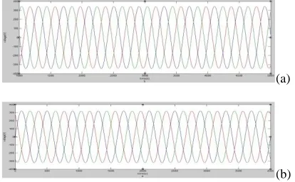
The distorted PCC voltages due to the feeder impedancewithout DVSI scheme are shown in Fig. 5(a). If these distortedvoltages are used for the reference current generationof AVSI, the current compensation will not be proper.
Therefore, the fundamental positive sequence of voltages isextracted from these distorted voltages using the algorithmexplained in Section III-A. These extracted voltages are givenin Fig. 5(b). These voltages are further used for the generationof inverter reference currents. Fig. 6(a)–(d) represents activepower demanded by load (Pl), active power supplied by grid(Pg), active power supplied by MVSI (Pμg), and active powersupplied by AVSI (Px), respectively. It can be observed that,from t = 0.1 to 0.4 s, MVSI is generating 4 kW power andthe load demand is 6 kW. Therefore, the remaining load activepower (2 kW) is drawn from the grid. During this period, the microgrid is operating in grid sharing mode. At t = 0.4 s, the microgrid power is increased to 7 kW, which is more than the load demand of 6 KW.
(a)
(b)
Fig.5. Without DVSI scheme: (a) PCC voltages
(b) fundamental positivesequence of PCC voltages.
(a)
(b)
(c)
(d)
Fig 6. Active power sharing: (a) load active power; (b) active power suppliedby grid; (c) active power supplied by
MVSI; and (d) active power supplied byAVSI.
This microgrid power change is consideredto show the change of operation of MVSI from gridsharing to grid injecting mode. Now, the excess power of 1 kWis injected to the grid and hence, the power drawn from grid isshown as negative. Fig. 7(a)–(c) shows the load reactive power(Ql), reactive power supplied by AVSI (Qx), and reactive powersupplied by MVSI (Qμg), respectively. It shows that total loadreactive power is supplied by AVSI, as expected.Fig. 8(a)–(d) shows the plots of load currents (il(abc)), currentsdrawn from grid (ig(abc)), currents drawn
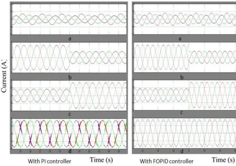
from MVSI(iμg(abc)), and currents drawn from the AVSI
(iμx(abc)),respectively. The load currents are unbalanced and
distorted.
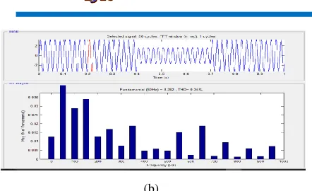
By using FOPID with DVSI scheme, the AVSI current harmonics are reduces and smoothening the wave forms shown in Fig.8(a)-(d). FOPID with DVSI scheme decreases the Total Harmonic Distortion (THD) shown in Fig.11(a) and (b).Advantages of FOPID with DVSI scheme are Power quality improvement and the following
• Reduction in harmonics
• Load voltage compensation
• Reactive power compensation
• It gives more power to the load
• Dc link voltage compensation
• Getting optimal values of kp and ki
• Minimize THD values and smoothening
waveforms
The MVSI supplies a balanced and sinusoidal current duringgrid supporting and grid injecting modes. The currents drawnfrom grid are also perfectly balanced and sinusoidal, as theauxiliary inverter compensates the unbalance and harmonics
Available online:
https://edupediapublications.org/journals/index.php/IJR/
P a g e
| 644
(b)
(c)
Fig.7. Reactive power sharing: (a) load reactive power; (b) reactive powersupplied by AVSI; and (c) reactive power supplied by MVSI.
Fig 8. Simulated performance of DVSI scheme: (a) load currents; (b) gridcurrents; (c) MVSI currents; and (d) AVSI
currents.
Fig. 9(a) shows the plot of fundamental positivesequence of PCC voltage (v+ta1) and grid current in phase-a(iga) during grid sharing and grid injecting modes. During gridsharing mode, this PCC voltage and grid current are in phaseand during grid injecting mode, they are out of phase. Fig. 9(b)establishes that MVSI current in phase-a is always in phasewith fundamental positive sequence of phase-a PCC voltage.The same is true for other two phases. Thus the compensationcapability of AVSI makes the source current and MVSI currentat unity power factor operation. The dc-link voltage of AVSI is shown in Fig. 10(a) and (b).
(a)
(b)
Fig 9. Grid sharing and grid injecting modes of operation: (a) PCC voltageand grid current (phase-a) and (b) PCC
voltage and MVSI current (phase-a).
(a)
(b)
Fig.10. (a) DC-link voltage of AVSI and (b) zoomed view of dc-link voltagedynamics during load change.
These figures indicate that thevoltage is maintained constant at a reference voltage (Vdcref ) of1040
V by the PI controller. All these simulation results presentedabove demonstrate the feasibility of DVSI for the loadcompensation as well as power injection from DG units in amicrogrid.
Available online:
https://edupediapublications.org/journals/index.php/IJR/
P a g e
| 645
(b)
Fig 11. % Total Harmonic Distortion of the Source Current (a) DVSI with PI Controller (b) DVSI with FOPID
CONCLUSION
A FOPID based DVSI scheme is proposed for microgrid systems with enhanced power quality. By using FOPID with DVSI scheme, the AVSI current harmonics are reduces and smoothening the wave forms. FOPID with DVSI scheme decreases the Total Harmonic Distortion (THD). The proposed scheme has the capability to exchange power from distributed generators (DGs) and also to compensate the local unbalanced and nonlinear load. Advantages of FOPID with DVSI scheme are Power quality improvement and the followingReduction in harmonics,Load voltage compensation,Reactive power compensation,It gives more power to the load,Getting optimal values of kp and ki, The performance of the proposed FOPID based DVSI scheme has been validated through simulation studies. Thus, aFOPID based DVSI scheme is a suitable interfacing option for microgrid supplying sensitive loads.the simulation results certified much better performance of FOPID controller in comparison with conventional PI controllers.
REFERENCES
[1] A. Kahrobaeian and Y.-R. Mohamed, “Interactive distributed generationinterface for flexible micro-grid operation in smart distribution systems,”IEEE Trans. Sustain. Energy, vol. 3, no. 2, pp. 295–305, Apr. 2012.
[2] N. R. Tummuru, M. K. Mishra, and S. Srinivas,
“Multifunctional VSCcontrolled microgrid using
instantaneous symmetrical components theory,”IEEE Trans. Sustain. Energy, vol. 5, no. 1, pp. 313–322, Jan.2014.
[3] Y. Zhang, N. Gatsis, and G. Giannakis, “Robust energy
managementfor microgrids with high-penetration
renewables,” IEEE Trans. Sustain.Energy, vol. 4, no. 4, pp. 944–953, Oct. 2013.
[4] R. Majumder, A. Ghosh, G. Ledwich, and F. Zare, “Load sharingand power quality enhanced operation of a distributed microgrid,” IETRenewable Power Gener., vol. 3, no. 2, pp. 109–119, Jun. 2009.
[5] J. Guerrero, P. C. Loh, T.-L. Lee, and M. Chandorkar, “Advanced controlarchitectures for intelligent microgrids— Part II: Power quality, energystorage, and ac/dc microgrids,” IEEE Trans. Ind. Electron., vol. 60, no. 4,pp. 1263–1270, Dec. 2013.
[6] Y. Li, D. Vilathgamuwa, and P. C. Loh, “Microgrid power qualityenhancement using a three-phase four-wire grid-interfacing compensator,”IEEE Trans. Ind. Appl., vol. 41, no. 6, pp. 1707–1719, Nov. 2005.
[7] M. Schonardie, R. Coelho, R. Schweitzer, and D. Martins, “Control ofthe active and reactive power using dq0 transformation in a three-phasegrid-connected PV system,” in Proc. IEEE Int. Symp. Ind. Electron., May2012, pp. 264–269.
[8] R. S. Bajpai and R. Gupta, “Voltage and power flow control of gridconnected wind generation system using
DSTATCOM,” in Proc. IEEEPower Energy Soc. Gen.
Meeting—Convers. Del. Elect. Energy 21stCentury, Jul.
2008, pp. 1–6.
[9] M. Singh, V. Khadkikar, A. Chandra, and R. Varma, “Grid interconnectionof renewable energy sources at the
distribution level withpower-quality improvement
features,” IEEE Trans. Power Del., vol. 26,no. 1, pp. 307– 315, Jan. 2011.
[10] H.-G. Yeh, D. Gayme, and S. Low, “Adaptive VAR control for distributioncircuits with photovoltaic generators,” IEEE Trans. Power Syst.,vol. 27, no. 3, pp. 1656–1663, Aug. 2012.
[11] C. Demoulias, “A new simple analytical method for calculating theoptimum inverter size in grid-connected PV plants,” Electr. Power Syst.Res., vol. 80, no. 10, pp. 1197– 1204, 2010.
[12] R. Tonkoski, D. Turcotte, and T. H. M. EL-Fouly, “Impact of high PVpenetration on voltage profiles in residential neighborhoods,” IEEETrans. Sustain. Energy, vol. 3, no. 3, pp. 518–527, Jul. 2012.[13] X. Yu and A.
Khambadkone, “Reliability analysis and cost
optimizationof parallel-inverter system,” IEEE Trans. Ind. Electron., vol. 59, no. 10,pp. 3881–3889, Oct. 2012.
Available online:
https://edupediapublications.org/journals/index.php/IJR/
P a g e
| 646
[14] A. Ghosh and A. Joshi, “A new approach to load balancing and powerfactor correction in power distribution system,” IEEE Trans. Power Del.,vol. 15, no. 1, pp. 417– 422, Jan. 2000.
[15] S. Iyer, A. Ghosh, and A. Joshi, “Inverter topologies for DSTATCOMapplications—A simulation study,” Electr. Power Syst. Res., vol. 75,no. 23, pp. 161–170, 2005.
[16] Y. Tang, P. C. Loh, P. Wang, F. H. Choo, and F. Gao, “Exploring inherentdamping characteristic of LCL filters for three-phase grid-connectedvoltage source inverters,”
IEEE Trans. Power Electron., vol. 27, no. 3,pp. 1433– 1443, Mar. 2012.
AUTHORS PROFILE.
Mr. ELAPA RAJENDRA is doing M.Tech Degree in Electrical Power Systems (EPS) fromSri Krishnadevaraya University college of Engineering and Technology, Ananthapuramu 515003,A.P,India, and hasgraduated his B.Tech from Audisankara College of Engineering and Technology,Gudur, A.P, India, and His areas of interest are Electrical power systems and electrical circuits.
Mr. N.RAJESHKUMAR GOWD has graduatedhis B.Tech from st.john’s College of Engg & Tech, Kurnool, A.P, India and M..Tech (EPE) from Bharath institute of
Engineering and TechnologyIbrahimpatnam,
Hyderabad,T.S,India. Presently he is working as Lecturer and HOD in Dept of EEE in Sri Krishnadevaraya University college of Engineering and Technology, Ananthapuramu-515003,A.P,India. He has published 7 International Journals & 3 National conferences .His research areas of interest are Electrical Power System-Smart grid, Reliability,Power electronics design.