Design and Analysis of Aging-Aware and Area
EfficientVedicMultiplier with Adaptive Hold
Logic
D.Vijayalakshmi
M.Tech- scholar,Chaitanya Institute of Science & Technology (CIST), Madhavapatnam. E-mail: [email protected]
Smts.Srividya
Associate professor ,Chaitanya Institute of Science & Technology (CIST), Madhavapatnam. E-mail :[email protected]
Abstract:
High speed, low power consumption is the key requirements to any VLSI design. The Area efficient multipliers play an important role. This paper presents an efficient implementation of a high speed, Vedic multiplier using aging aware technique and adaptive hold logic. This study presented the design and implementation of Vedic multipliers using XILINX. In this work, Modified Vedic multiplier is having least area. The Modified Vedic multiplier with adaptive hold logic and aging awareness make this efficient and also reliable. 32 bit signed multiplication and fractional multiplication is carried out and verified with around 10000 test patterns.
Keywords: Delay, Vedic Multiplier, Aging Aware, Adaptive hold.
I.Introduction
Multiplication is one of the most widely used arithmetic operations. Due to this a wide range of multiplier architectures are reported in the literature providing flexible choices for various applications. Among them the simplest is array multiplier [1] which is also the slowest. Some high performance multipliers are presented in
[3-6]. Multiplication [4] is the most important arithmetic operation in signal processing applications. All the signal and data processing operations involve multiplication. As speed is always a constraint in the multiplication operation, increase in speed can be achieved by reducing the number of steps in the computation process. The speed of multiplier determines the efficiency of such a system. In any system design, the three main constraints which determine the performance of the system are speed, area and power requirement.
Thus, integrating Vedic mathematics for the multiplier design will enhance the speed of multiplication operation.
II. Literature Survey
Traditional circuits use critical path delay as the overall circuit clock cycle in order to perform correctly. However, the probability that the critical paths are activated is low. In mostcases, the path delay is shorter than the critical path. For these Noncritical paths, using the critical path delay as the overall cycle period will result in significant timing waste. Hence,the variable-latency design was proposed to reduce the timing waste of traditional circuits. The variable-latency design divides the circuit into twoparts: 1) shorter paths and 2) longer paths. Shorter paths can execute correctly in one cycle, whereas longer pathsneed two cycles to execute. When shorter paths are activated frequently, the average latency of variable-latency designs isbetter than that of traditional designs. For example, several variable-latency adders were proposed using the speculation technique with error detection and recovery [8].
A short path activation function algorithm was proposed in [9] to improve the accuracy of the hold logic and to optimize theperformance of the variable-latency circuit. An instruction scheduling algorithm was proposed in [10] to schedule the Operations on no uniform latency functional units and improvethe performance of Very Long Instruction Word processors. In [11], a variable-latency pipelined multiplier architecture witha Booth algorithm was proposed.
In [12], process-variation tolerant architecture for arithmetic units was proposed, where the effect of process-variation is considered to increase the circuit yield. In addition, the critical paths are divided into two shorter paths that could be unequal and the clock cycleis set to the delay of
the longer one. These research designs were able to reduce the timing waste of traditional circuits to improve performance, but they did not consider the aging effect and could not adjust themselves during the runtime. Avariable-latency adder design that considers the aging effect was proposed in [13] and [14]. However, no variable-latency multiplier design that considers the aging effect and can adjust dynamically has been done.
III. Design of Vedic Multiplier
As discussed in the previous section, the critical pathdelay of the Multiplier depends on the computation time ofadder and multiplier. In this section, we have discussed an efficient architecture for adder and multiplier using modified Ripple Carry adder.
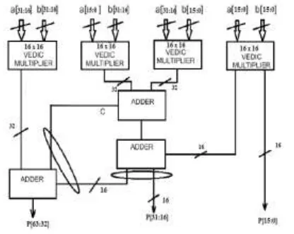
The 32-bit multiplier is designed using four 16x16 Vedic multipliers which employ Urdhva Tiryagbhyam sutra and carry skip technique for partial product addition. The output of these Vedic multipliers is added by modifying the logic levels of ripple carry adder. Block diagram of the proposed 32x32multiplier is illustrated in figure 1.
is added to the overlapping sum using ADDER-2 which gives the product P[31:16]. Finally, MSB bits P[63:32] are obtained by adding the fourth multiplier output to the carry from ADDER-1 (added at the fifth bit position) and higher order bits (acts as lower nibble of addend) of ADDER-3.
Fig 1Block diagram of 32x32 multiplier.
IV. Proposed Aging Aware Multiplier
Architecture
This section details the proposed aging-aware reliable multiplier design. It introduces the overall architecture and thefunctions of each component and also describes how to design AHL that adjusts the circuit when significant aging occurs.
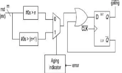
Fig 2: Proposed aging aware Vedic multiplier
Fig 2, shows our proposed aging-aware multiplier architecture, which includes two m-bit inputs (m is a positive number), one 2m-bit output, one
Vedic multiplier, 2m 1-bit Razor flip-flops [16],
and an AHL circuit. The inputs of the
row-bypassing multiplier are the symbols in the parentheses.In the proposed architecture, Vedic
multiplier can be examined by the number of zeros in either the multiplicand or multiplicator to predict whether the operation requires one cycle or two cycles to complete. When input patterns are random, the number of zeros and ones in the multiplicator and multiplicand follows a normal distribution. Therefore, using the number of zeros or ones as the judging criteria results in similar outcomes. Hence, the two aging-aware multipliers can be implemented using similar architecture, and the difference between the two bypassing multipliers lies in the input signals of the AHL. According to the bypassing selection in the column or row-bypassing multiplier, the input signal of the AHL in the architecture with the column-bypassing multiplier is the multiplicand, whereas that of the row-bypassing multiplier is the multiplicator. Razor flip-flops can be used to detect whether timing violations occur before the next input pattern arrives.
Fig. 3: Razor flip flops
If errors occur, the Razor flip-flop will set the error signal to 1 to notify the system to re execute the operation and notify the AHL circuit that an error has occurred. We use Razor flip-flops to detect whether an operation that is considered to be a one-cycle pattern can really finish in a cycle. If not, the operation is re executed with two cycles.
Fig 4: Diagram of AHL (md means multiplicand; mr means multiplicator).
Although the reexecution may seem costly, the overall cost is low because the reexecution frequency is low. More details for the Razor flip -flop can be found in [17]. The AHL circuit is the key component in the aging-aware variable - latency multiplier. Fig. 4 shows the details of the AHL circuit. The AHL circuit contains an aging indicator, two judging blocks, one mux, and one D flip-flop. The aging indicator indicates whether the circuit has suffered significant performance degradation due to the aging effect. The aging indicator is implemented in a simple counter that counts the number of errors over a certain amount
of operations and is reset to zero at the end of those operations.
If the cycle period is too short, the column-or row-bypassing multiplier is not able to complete these operations successfully, causing timing violations. These timing violations will be caught by the Razor flip-flops, which generate error signals. If errors happen frequently and exceed a predefined threshold, it means the circuit has suffered significant timing degradation due to the aging effect, and the aging indicator will output signal 1; otherwise, it will output 0 to indicate the aging effect is still not significant, and no actions are needed.
Results
RTL Schematic
Fig 5 RTL Schematic of Aging Aware Vedic Multiplier
Fig 6 Simulation result of Aging Aware Vedic Multiplier
C) Comparison Table
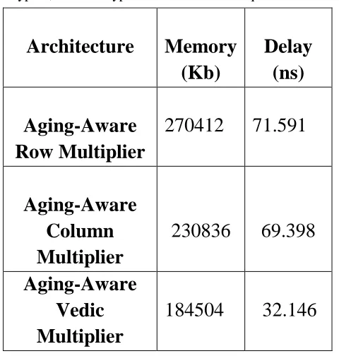
Table I Comparison of Aging-Aware Multiplier with Row bypass, Column bypass and Vedic Techniques
Conclusion
This paper proposed an aging-aware multiplier design with the AHL. The multiplier is able to adjust the AHL to mitigate performance
degradation due to increased delay. The experimental results show that our proposed architecture with 32×32 Vedic multiplier is Delay efiicient. The Proposed aging-aware Vedic multiplier with Adaptive hold logic Architecture was synthesized and simulated in Xilinx and Modelsim software respectively.
References
[1] N. H. E. Weste and D. M. Harris, Integrated Circuit Design,Pearson, 2010.
[2] Swami Bharati Krishna Tirthaji Maharaja, “Vedic Mathematics”, MotilalBanarsidass Publishers, 1965.
[3] Rakshith T R and RakshithSaligram, “Design of High Speed Low Power Multiplier using Reversible logic: a Vedic Mathematical Approach”, International Conference on Circuits, Power and Computing Technologies (ICCPCT-2013), ISBN: 978-1-4673-4922-2/13, pp.775-781.
[4] M.E. Parama sivam and Dr. R.S. Sabeenian, “An
Efficient Bit Reduction Binary Multiplication
Algorithm using Vedic Methods”, IEEE 2nd
International Advance Computing Conference, 2010, ISBN: 978-1-4244-4791-6/10, pp. 25-28.
[5] Sushma R. Huddar, SudhirRaoRupanagudi, Kalpana M and Surabhi Mohan, “Novel High Speed Vedic Mathematics Multiplier using Compressors”, International Multi conference on Automation, Computing, Communication, Control and Compressed Sensing(iMac4s), 22 23 March 2013, Kottayam, ISBN: 978-1-4673-5090-7/13, pp.465-469.
[6] L. Sriraman and T. N. Prabakar, “Design and Implementation of Two Variables Multiplier Using
KCM and Vedic Mathematics”, 1st
International Conference on Recent Advances in Information Technology (RAIT -2012), ISBN: 978-1-4577-0697-4/12.
Architecture
Memory
(Kb)
Delay
(ns)
Aging-Aware
Row Multiplier
270412
71.591
Aging-Aware
Column
Multiplier
230836
69.398
Aging-Aware
Vedic
Multiplier
[6] C. S.Wallace, “A suggestion for a fast multiplier,” IEEE Transactions on Electronic Computers, vol. EC-13, no. 1, pp. 14–17, 1964.
[7] R. S. Waters and E. E. Swartzlander, “A reduced complexity wallace multiplier reduction,” IEEE Transactions on Computers, vol. 59, no. 8, pp. 1134– 1137, 2010.
[8] K. Du, P. Varman, and K. Mohanram, “High performance reliable variable latency carry select addition,” in Proc. DATE, 2012, pp. 1257–1262.
[9] Y.-S. Su, D.-C.Wang, S.-C. Chang, and M.
Marek-Sadowska, “Performance” optimization using
variable-latency design style,” IEEE Trans. Very Large Scale Integr. (VLSI) Syst., vol. 19, no. 10, pp. 1874–1883, Oct. 2011.
[10] N. V. Mujadiya, “Instruction scheduling on
variable latency functional units of VLIW
processors,” in Proc. ACM/IEEE ISED, Dec. 2011, pp. 307–312.
[11] M. Olivieri, “Design of synchronous and asynchronous variable-latency pipelined multipliers,” IEEE Trans. Very Large Scale Integr. (VLSI) Syst., vol. 9, no. 4, pp. 365–376, Aug. 2001.
[12] D. Mohapatra, G. Karakonstantis, and K. Roy, “Low-power process variation tolerant arithmetic units using input-based elastic clocking,” in Proc. ACM/IEEE ISLPED, Aug. 2007, pp. 74–79.
[13] Y. Chen, H. Li, J. Li, and C.-K.Koh, “Variable-latency adder (VL-Adder): New arithmetic circuit design practice to overcome NBTI,” inProc. ACM/IEEE ISLPED, Aug. 2007, pp. 195–200.
[14] Y. Chen et al., “Variable-latency adder (VL-Adder) designs for low power and NBTI tolerance,” IEEE Trans. Very Large Scale Integr. (VLSI) Syst., vol. 18, no. 11, pp. 1621–1624, Nov. 2010.
[15] ShahzadAsif and Yinan Kong, “Low Area Wallace Multiplier”,VLSI Design, vol. 2014, Article ID 343960, 6 pages.
[16] Ing-Chao Lin, Member, IEEE, Yu-Hung Cho,
and Yi-Ming Yang, “Aging-Aware Reliable
Multiplier Design With Adaptive Hold Logic”, IEEE transactions on very large scale integration (vlsi) systems, vol. 23, no. 3, March 2015