Single Board Computers
Programmer’s Reference Guide
(Part 1 of 2)
Notice
While reasonable efforts have been made to assure the accuracy of this document, Motorola, Inc. assumes no liability resulting from any omissions in this document, or from the use of the information obtained therein. Motorola reserves the right to revise this document and to make changes from time to time in the content hereof without obligation of Motorola to notify any person of such revision or changes.
No part of this material may be reproduced or copied in any tangible medium, or stored in a retrieval system, or transmitted in any form, or by any means, radio, electronic, mechanical, photocopying, recording or facsimile, or otherwise, without the prior written permission of Motorola, Inc.
It is possible that this publication may contain reference to, or information about Motorola products (machines and programs), programming, or services that are not announced in your country. Such references or information must not be construed to mean that Motorola intends to announce such Motorola products, programming, or services in your country.
Restricted Rights Legend
If the documentation contained herein is supplied, directly or indirectly, to the U.S. Government, the following notice shall apply unless otherwise agreed to in writing by Motorola, Inc.
Use, duplication, or disclosure by the Government is subject to restrictions as set forth in subparagraph (c)(1)(ii) of the Rights in Technical Data and Computer Software clause at DFARS 252.227-7013.
Motorola, Inc. Computer Group 2900 South Diablo Way
Preface
This manual provides board level information and detailed ASIC chip information including register bit descriptions for the MVME166, MVME167, MVME176, MVME177, and MVME187 Single Board Computers. The information in this manual applies to the single board computers listed in the following table:
Notes
This document is bound in two parts. Part 1 (VMESBCA1/PGcontains Chapters 1 through 4. Part 2 (VMESBCA2/PGxx))contains Chapters 5 through 9.
This manual replaces the MVME166/167/187 Single Board Computers ProgrammerÕs Reference Guide, MVME187PG/D3, and its supplement, MVME187PG/D3A1. They are obsolete.
This manual is intended for anyone who wants to program these boards in order to design OEM systems, supply additional capability to an existing compatible system, or work in a lab environment for experimental purposes.
A basic knowledge of computers and digital logic is assumed.
To use this manual, you should be familiar with the publications listed in Related MVME166
Models
MVME167 Models
MVME176 Models
MVME177 Models
MVME187 Models MVME166-011a MVME167-001a MVME176-001a MVME177-001a MVME187-001a MVME166-012a MVME167-002a MVME176-002a MVME177-002a MVME187-002a MVME166-013a MVME167-003a MVME176-003a MVME177-003a MVME187-003a MVME166-014a MVME167-004a MVME176-004a MVME177-004a MVME187-004a MVME166-015a MVME167-031a MVME176-005a MVME177-005a MVME187-023a MVME166-016a MVME167-032a MVME176-006a MVME177-006a MVME187-024a
MVME167-033a MVME177-011a MVME187-031a
MVME167-034a MVME177-012a MVME187-032a
MVME167-035a MVME177-013a MVME187-033a
MVME167-036a MVME177-014a MVME187-034a
Related Documentation
The following publications are applicable to the Single Board Computers and may provide additional helpful information. If not shipped with this product, they may be purchased by contacting your local Motorola sales ofÞce. Non-Motorola documents may be obtained from the sources listed.
Document Title Publication NumberMotorola
MVME166 Single Board Computer User's Manual MVME166/D MVME167 Single Board Computer User's Manual MVME167/D MVME176 Single Board Computer Installation and Use Manual VME176A/IH MVME177 Single Board Computer Installation and Use Manual VME177A/IH MVME167Bug Debugging Package User's Manual MVME167BUG/D MVME177Bug Diagnostics User's Manual V177DIAA/UM Debugging Package for Motorola 68K CISC CPUs User's
Manual (Parts 1 and 2)
68KBUG1/D and 68KBUG2/D MVME187 RISC Single Board Computer User's Manual MVME187/D MVME187Bug Debugging Package User's Manual MVME187BUG/D Debugging Package for Motorola 88K RISC CPUs User's
Manual
88KBUG1/D and 88KBUG2/D Single Board Computers SCSI Software User's Manual SBCSCSI/D MVME712-06/07/09 I/O Distribution Board Set User's Manual MVME712IO/D MVME712-10 Transition Module User's Manual MVME712-10/D MVME712M Transition Module and P2 Adapter Board
User's Manual
MVME712M/D MVME712-12, MVME712-13, MVME712A, MVME712AM,
and MVME712B Transition Modules and LCP2 Adapter Board User's Manual
Note
Although not shown in the above list, each Motorola ComputerGroup manual publication number is suffixed with characterswhich represent the revision level of the document, such as Ò/xx2Ó (the second revision of a manual); a supplement bears the same number as a manual but has a suffix such as Ò/xx2A1Ó (the first supplement to the second edition of the manual).
The following publications are available from the sources indicated:
Versatile Backplane Bus: VMEbus, ANSI/IEEE Std 1014-1987, The Institute of Electrical and Electronics Engineers, Inc., 345 East 47th Street, New York, NY 10017 (VMEbus SpeciÞcation). (This is also Microprocessor System Bus for 1 to 4 Byte Data, IEC 821 BUS, Bureau Central de la Commission Electrotechnique Internationale; 3, rue de VarembŽ, Geneva, Switzerland.)
Z85230 Serial Communications Controller Data Sheet, order number DC-8293-02, Zilog Inc., 210 East Hacienda Drive, Campbell, CA 95008-6600.
IEEE Standard for Multiplexed High-Performance Bus Structure: VSB, ANSI/IEEE Std 1096-1988, The Institute of Electrical and Electronics Engineers, Inc., 345 East 47th Street, New York, NY 10017 (VSB SpeciÞcation). (This is also Parallel Sub-system Bus of the IEC 821 VMEbus, IEC 822 VSB, Bureau Central de la Commission
Electrotechnique Internationale; 3, rue de VarembŽ, Geneva, Switzerland.)
ANSI Small Computer System Interface-2 (SCSI-2), Draft Document X3.131-198X, Revision 10c; Global Engineering Documents, 15 Inverness Way East, Englewood, CO 80112-5704.
CL-CD2400/2401 Four-Channel Multi-Protocol Communications Controller Data Sheet, order number 542400-003; Cirrus Logic, Inc., 3100 West Warren Ave., Fremont, CA 94538.
MC88100 RISC Microprocessor User's Manual MC88100UM MC88200 Cache/Memory Management Unit (CMMU)
User's Manual
MC88200UM M68040 Microprocessors User's Manual M68040UM M68060 Microprocessors User's Manual M68060UM
M68000 Family Reference Manual M68000FR
82596CA Local Area Network Coprocessor Data Sheet, order number 290218; and 82596 User's Manual, order number 296853; Intel Corporation, Literature Sales, P.O. Box 58130, Santa Clara, CA 95052-8130.
DS1643 Nonvolatile Timekeeping RAM, Dallas Semiconductor Data Manual, 4401 South Beltwood Parkway, Dallas, Texas 75244-3292.
NCR 53C710 SCSI I/O Processor Data Manual, order number NCR53C710DM, and NCR 53C710 SCSI I/O Processor ProgrammerÕs Guide, order number NCR53C710PG; NCR Corporation, Microelectronics Products Division, 1635 Aeroplaza Dr., Colorado Springs, CO 80916.
MK48T08(B)/MK48T18(B) TimekeeperTM and 8Kx8 ZeropowerTMRAM data sheet in Static RAMs Databook, order number DBSRAM71; SGS-THOMSON
Microelectronics; North & South American Marketing Headquarters, 1000 East Bell Road, Phoenix, AZ 85022-2699.
i28F008 Flash Memory Data Sheet, order number 290435, i28F020 Flash MemoryData Sheet, order number 290245, i28F008SA Software Drivers Application Note, order number 292095, and i28F008SA Automation and Algorithms Application Note, order number 292099; Intel Literature Sales, P.O. Box 7641, Mt. Prospect, IL 60056-7641.
MC68230 Parallel Interface Timer (PI/T) Data Sheet, order number MC68230/D, Motorola Semiconductor Products, Inc., LDC, Broadway Bldg. BB100, P.O. Box 20924, Phoenix, AZ 85036-0924.
Manual Terminology
Throughout this manual, a convention is used which precedes data and address parameters by a character identifying the numeric format as follows:
For example, Ò12Ó is the decimal number twelve, and Ò$12Ó is the decimal number eighteen.
Unless otherwise speciÞed, all address references are in hexadecimal.
An asterisk (*) following the signal name for signals which are level signiÞcant denotes that the signal is true or valid when the signal is low.
$ % &
dollar percent ampersand
An asterisk (*) following the signal name for signals which are edge signiÞcant denotes that the actions initiated by that signal occur on high to low transition.
In this manual, assertion and negation are used to specify forcing a signal to a particular state. In particular, assertion and assert refer to a signal that is active or true; negation and negate indicate a signal that is inactive or false. These terms are used independently of the voltage level (high or low) that they represent.
Data and address sizes are deÞned as follows:
❏ A byte is eight bits, numbered 0 through 7, with bit 0 being the least significant. ❏ A two-byte is 16 bits, numbered 0 through 15, with bit 0 being the least
significant. For the MVME166, MVME167, MVME176, MVME177, and other CISC boards, this is called a word. For the MVME187 and other RISC boards, this is called a half-word.
❏ A four-byte is 32 bits, numbered 0 through 31, with bit 0 being the least
significant. For the MVME166, MVME167, MVME176, MVME177, and other CISC boards, this is called a longword. For the MVME187 and other RISC boards, this is called a word.
Throughout this manual, it is assumed that the MPU on the MVME187 always programs the CMMUs with big-endian byte ordering, as shown below. Any attempt to use small-endian byte ordering immediately renders the MVME187Bug
debugger unusable.
The terms control bit and status bit are used extensively in this document:
BIT
31 24 23 16 15 08 07 00
ADR0 ADR1 ADR2 ADR3
control bit A bit in a register that can be set and cleared under software control.
true Indicates that a bit is in the state that enables the function it controls
false Indicates that the bit is in the state that disables the function it controls
In all tables, the terms 0 and 1 are used to describe the actual value that should be written to the bit, or the value that it yields when read.
The computer programs stored in the Read Only Memory of this device contain material copyrighted by Motorola Inc., Þrst published 1990, and may be used only under a license such as the License for Computer Programs (Article 14) contained in Motorola's Terms and Conditions of Sale, Rev. 1/79.
!
WARNING
This equipment generates, uses, and can radiate magnetic energy. It may cause or be susceptible to electro-magnetic interference (EMI) if not installed and used in a cabinet with adequate EMI protection.
Motorola¨ and the Motorola symbol are registered trademarks of Motorola, Inc.
Delta Series, SYSTEM V/68, SYSTEM V/88, VMEmodule, and VMEsystem are trademarks of Motorola, Inc.
Timekeeper and Zeropower are trademarks of SGS-THOMSON Microelectronics.
All other products mentioned in this document are trademarks or registered trademarks of their respective holders.
© Copyright Motorola 1995, 1996
All Rights Reserved
Printed in the United States of America
Contents
Chapter 1 Programming Issues
Introduction...1-1
Programming Interfaces...1-1
MC68040 MPU...1-2
MC68060 MPU...1-2
M88000 MPU...1-2
Data Bus Structure...1-2
EPROMs on the MVME167/176/177/187...1-3
MVME167 and MVME187 ... 1-3 MVME176/177 ... 1-3
Flash Memory on the MVME176/177...1-4
Flash Memory and Download EPROM on the MVME166...1-5
SRAM...1-6
Onboard DRAM...1-7
Battery Backed Up RAM and Clock...1-7
VMEbus Interface...1-8
VME Subsystem Bus (VSB) Interface...1-8
I/O Interfaces...1-8
Serial Port Interface... 1-8 MC68230 Parallel Interface/Timer (MVME166/176 Only) ... 1-10 Parallel (Printer) Interface... 1-12 Ethernet Interface ... 1-12 SCSI Interface... 1-13
Local Resources...1-14
Programmable Tick Timers ... 1-14 Watchdog Timer... 1-14 Software-Programmable Hardware Interrupts ... 1-14 Local Bus Time-out ... 1-14
Interrupt Handling...1-15
Interrupt Programming Examples...1-16
M68000 VMEchip2 Tick Timer 1 Periodic Interrupt Example ... 1-17 MVME187 Interrupt Handling... 1-19
Cache Coherency, MVME176/177... 1-23
Cache Coherency, MVME187... 1-24
Using Bus Timers... 1-24
Indivisible Cycles... 1-26
No Supervisor Stack Pointer on MC68060... 1-27
Sources of Local BERR*... 1-27
Local Bus Time-out... 1-28
VMEbus Access Time-out... 1-28
VMEbus BERR*... 1-28
Local DRAM Parity Error... 1-28
VMEchip2... 1-28
VSBchip2 BERR*... 1-29
Bus Error Processing... 1-29
Error Conditions... 1-29
MPU Parity Error... 1-30
MPU Offboard Error... 1-30
MPU TEA - Cause UnidentiÞed... 1-30
MPU Local Bus Time-out... 1-31
DMAC VMEbus Error... 1-31
DMAC Parity Error... 1-31
DMAC Offboard Error... 1-32
DMAC LTO Error... 1-32
DMAC TEA - Cause UnidentiÞed... 1-32
SCC Retry Error... 1-34
SCC Parity Error... 1-34
SCC Offboard Error... 1-34
SCC LTO Error... 1-36
LAN Parity Error... 1-36
LAN Offboard Error... 1-36
LAN LTO Error... 1-37
SCSI Parity Error... 1-37
SCSI Offboard Error... 1-37
SCSI LTO Error... 1-38
Chapter 2 Hardware Configuration
Introduction... 2-1
SCSI Termination... 2-1
Fuses...2-2
MVME166 Fuses...2-3
MVME176 Polyswitches...2-3
MVME167/177/187 Fuses...2-3
ConÞguration Jumpers...2-4
ConÞguration Jumpers, MVME166...2-5
ConÞguration Jumpers, MVME167...2-8
ConÞguration Jumpers, MVME177...2-12
ConÞguration Jumpers, MVME187...2-16
ConÞguration Jumpers, MVME176...2-20
Chapter 3 Memory Maps
Introduction...3-1
VMEbus Memory Map...3-1
VSB Memory Map...3-2
Local Bus Memory Map...3-2
Normal Address Range...3-2
Detailed I/O Memory Maps...3-3
Chapter 4 VMEchip2
Introduction...4-1
Summary of Features...4-1
Functional Blocks...4-4
Local Bus to VMEbus Interface...4-4
Local Bus to VMEbus Requester ... 4-8
VMEbus to Local Bus Interface...4-9
Local Bus to VMEbus DMA Controller... 4-11
DMAC VMEbus Requester... 4-13
Tick and Watchdog Timers...4-14
Prescaler... 4-14 Tick Timer ... 4-14 Watchdog Timer... 4-15
VMEbus Interrupter...4-16
VMEbus System Controller...4-17
Reset Driver 4-18
Local Bus Interrupter and Interrupt Handler... 4-18
Global Control and Status Registers... 4-20
VMEboard Functions... 4-20
LCSR Programming Model... 4-21
Programming the VMEbus Slave Map Decoders... 4-26
VMEbus Slave Ending Address Register 1 ... 4-29 VMEbus Slave Starting Address Register 1 ... 4-29 VMEbus Slave Ending Address Register 2 ... 4-29 VMEbus Slave Starting Address Register 2 ... 4-30 VMEbus Slave Address Translation Address Offset Register 1 ... 4-30 VMEbus Slave Address Translation Select Register 1... 4-31 VMEbus Slave Address Translation Address Offset Register 2 ... 4-32 VMEbus Slave Address Translation Select Register 2 ... 4-32 VMEbus Slave Write Post and Snoop Control Register 2... 4-33 VMEbus Slave Address Modifier Select Register 2 ... 4-34 VMEbus Slave Write Post and Snoop Control Register 1... 4-35 VMEbus Slave Address Modifier Select Register 1 ... 4-36
Programming the Local Bus to VMEbus Map Decoders... 4-37
Local Bus Slave (VMEbus Master) Ending Address Register 1 .... 4-40 Local Bus Slave (VMEbus Master) Starting Address Register 1 ... 4-40 Local Bus Slave (VMEbus Master) Ending Address Register 2 .... 4-40 Local Bus Slave (VMEbus Master) Starting Address Register 2 ... 4-41 Local Bus Slave (VMEbus Master) Ending Address Register 3 .... 4-41 Local Bus Slave (VMEbus Master) Starting Address Register 3 ... 4-41 Local Bus Slave (VMEbus Master) Ending Address Register 4 .... 4-42 Local Bus Slave (VMEbus Master) Starting Address Register 4 ... 4-42 Local Bus Slave (VMEbus Master) Address Translation
Address Register 4 ... 4-42 Local Bus Slave (VMEbus Master) Address Translation
Local Bus To VMEbus I/O Control Register ... 4-48 ROM Control Register ... 4-49
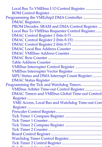
Programming the VMEchip2 DMA Controller...4-52
DMAC Registers... 4-53 PROM Decoder, SRAM and DMA Control Register ... 4-54 Local Bus To VMEbus Requester Control Register... 4-56 DMAC Control Register 1 (bits 0-7) ... 4-57 DMAC Control Register 2 (bits 8-15) ... 4-59 DMAC Control Register 2 (bits 0-7) ... 4-60 DMAC Local Bus Address Counter ... 4-61 DMAC VMEbus Address Counter... 4-62
DMAC Byte Counter ... 4-62
Table Address Counter ... 4-63 VMEbus Interrupter Control Register ... 4-63 VMEbus Interrupter Vector Register ... 4-64 MPU Status and DMA Interrupt Count Register ... 4-65 DMAC Status Register ... 4-66
Programming the Tick and Watchdog Timers...4-67
VMEbus Arbiter Time-out Control Register ... 4-67 DMAC Timers and VMEbus Global Time-out Control
Register ... 4-68 VME Access, Local Bus and Watchdog Time-out Control
Register ... 4-69 Prescaler Control Register... 4-70 Tick Timer 1 Compare Register ... 4-71 Tick Timer 1 Counter... 4-71 Tick Timer 2 Compare Register ... 4-72 Tick Timer 2 Counter... 4-72 Board Control Register... 4-73 Watchdog Timer Control Register... 4-74 Tick Timer 2 Control Register ... 4-75 Tick Timer 1 Control Register ... 4-76 Prescaler Counter ... 4-76
Programming the Local Bus Interrupter...4-77
Local Bus Interrupter Enable Register (bits 24-31)... 4-84 Local Bus Interrupter Enable Register (bits 16-23)... 4-85 Local Bus Interrupter Enable Register (bits 8-15)... 4-86 Local Bus Interrupter Enable Register (bits 0-7)... 4-87 Software Interrupt Set Register (bits 8-15) ... 4-88 Interrupt Clear Register (bits 24-31)... 4-88 Interrupt Clear Register (bits 16-23)... 4-89 Interrupt Clear Register (bits 8-15)... 4-90 Interrupt Level Register 1 (bits 24-31)... 4-90 Interrupt Level Register 1 (bits 16-23)... 4-91 Interrupt Level Register 1 (bits 8-15)... 4-91 Interrupt Level Register 1 (bits 0-7)... 4-92 Interrupt Level Register 2 (bits 24-31)... 4-92 Interrupt Level Register 2 (bits 16-23)... 4-93 Interrupt Level Register 2 (bits 8-15)... 4-93 Interrupt Level Register 2 (bits 0-7)... 4-94 Interrupt Level Register 3 (bits 24-31)... 4-94 Interrupt Level Register 3 (bits 16-23)... 4-95 Interrupt Level Register 3 (bits 8-15)... 4-95 Interrupt Level Register 3 (bits 0-7)... 4-96 Interrupt Level Register 4 (bits 24-31)... 4-96 Interrupt Level Register 4 (bits 16-23)... 4-97 Interrupt Level Register 4 (bits 8-15)... 4-97 Interrupt Level Register 4 (bits 0-7)... 4-98 Vector Base Register ... 4-98 I/O Control Register 1 ... 4-99 I/O Control Register 2 ... 4-100 I/O Control Register 3 ... 4-104 Miscellaneous Control Register ... 4-105
GCSR Programming Model... 4-107
Programming the GCSR... 4-109
General Purpose Register 3... 4-115 General Purpose Register 4... 4-116 General Purpose Register 5... 4-116
Chapter 5 VSBchip2
Introduction...5-1
Summary of Features...5-1
Functional Description...5-3
VSB to Local Bus Interface...5-5
VSB Slave Interface ... 5-5 Programmable Map Decoders ... 5-5 Write Post Buffer ... 5-6 Local Bus Master Interface... 5-6 VSB Block Transfer to a Local Bus Burst ... 5-8
Local Bus to VSB Interface...5-8
Local Bus Slave Interface... 5-9 Programmable Map Decoders ... 5-9 Bounce Mode ... 5-9 Write Post Buffer ... 5-10 VSB Master Interface ... 5-11 VSB Dynamic Bus Sizing... 5-11 VSB Timers... 5-11 VSB Block Transfers... 5-12
VSB Requester and VSB Serial Arbiter...5-13
VSB Geographical Addressing... 5-13 VSB Requesters... 5-14 VSB Serial Arbiter ... 5-16 Arbitration Timer ... 5-16
VSB Interrupter...5-16
VSB Interrupt Handler...5-18
Local Bus Interrupter...5-18
Control and Status Registers...5-19
Local Control and Status Registers Programming Model...5-20
Chip Control/Status Register...5-23
Local Interrupt Vector Base Register...5-25
Local Interrupt Status Register...5-26
Reserved Register... 5-30
VSB Requester Control/Status Register... 5-31
Timer Control Register... 5-33
Timer Clock Prescaler Register... 5-34
Local Bus Slave 1 Address Range Register... 5-35
Local Bus Slave 1 Address Offset Register... 5-36
Local Bus Slave 1 Attribute Register... 5-36
Local Bus Slave 2 Address Range Register... 5-38
Local Bus Slave 2 Address Offset Register... 5-39
Local Bus Slave 2 Attribute Register... 5-39
Local Bus Slave 3 Address Range Register... 5-41
Local Bus Slave 3 Address Offset Register... 5-42
Local Bus Slave 3 Attribute Register... 5-42
Local Bus Slave 4 Address Range Register... 5-44
Local Bus Slave 4 Address Offset Register... 5-45
Local Bus Slave 4 Attribute Register... 5-45
Reserved Registers... 5-46
Local Error Address Register... 5-47
Prescaler Current Count Register... 5-47
Prescaler Test Register... 5-48
Board Control and Status Registers Programming Model... 5-50
EVSB Attention Register... 5-52
EVSB Test and Set (TAS) Register... 5-54
General Purpose Register 1... 5-55
General Purpose Register 2... 5-55
VSB Error Status Register... 5-56
VSB Interrupt Control Register... 5-57
VSB Interrupt Vector Register... 5-58
VSB Interrupt Enable Register... 5-59
VSB Interrupt Status Register... 5-60
VSB Slave 1 Address Range Register... 5-61
VSB Slave 1 Address Offset Register... 5-61
VSB Slave 1 Attribute Register... 5-62
VSB Slave 2 Address Range Register... 5-65
VSB Slave 2 Address Offset Register... 5-65
VSB Slave 2 Attribute Register... 5-66
Reserved Register... 5-69
Chapter 6 PCCchip2
Introduction...6-1
Summary of Major Features...6-1
Functional Description...6-2
General Description...6-2
BBRAM Interface...6-3
Download ROM Interface (MVME166 Only)...6-3
82596CA LAN Controller Interface...6-4
MPU Port and MPU Channel Attention... 6-4 MC68040-Bus Master Support for 82596CA ... 6-5 LANC Bus Error ... 6-5 LANC Interrupt... 6-6
53C710 SCSI Controller Interface...6-7
Memory Controller MEMC040 Interface...6-7
Parallel Port Interface...6-7
General Purpose I/O Pin...6-8
CD2401 SCC Interface...6-8
Interrupt Prioritizer (MVME187)...6-10
Tick Timer... 6-11
Overall Memory Map...6-12
Programming Model...6-13
Chip ID Register...6-16
Chip Revision Register...6-16
General Control Register...6-17
Vector Base Register...6-18
Programming the Tick Timers...6-20
SCC Error Status Register and Interrupt Control Registers... 6-29
SCC Error Status Register ... 6-29 SCC Modem Interrupt Control Register ... 6-30 SCC Transmit Interrupt Control Register ... 6-31 SCC Receive Interrupt Control Register... 6-32 Modem PIACK Register ... 6-33 Transmit PIACK Register ... 6-34 Receive PIACK Register... 6-35
LANC Error Status and Interrupt Control Registers... 6-36
LANC Error Status Register ... 6-36 82596CA LANC Interrupt Control Register ... 6-37 LANC Bus Error Interrupt Control Register ... 6-38
Programming the SCSI Error Status and Interrupt Registers... 6-39
SCSI Error Status Register ... 6-39 SCSI Interrupt Control Register... 6-40
Programming the Printer Port... 6-41
Printer ACK Interrupt Control Register ... 6-41 Printer FAULT Interrupt Control Register ... 6-42 Printer SEL Interrupt Control Register... 6-43 Printer PE Interrupt Control Register ... 6-44 Printer BUSY Interrupt Control Register ... 6-45 Printer Input Status Register ... 6-46 Printer Port Control Register... 6-47 Chip Speed Register ... 6-48 Printer Data Register ... 6-49 Interrupt Priority Level Register ... 6-50 Interrupt Mask Level Register ... 6-51
Chapter 7 MEMC040
Introduction... 7-1
Summary of Features... 7-1
Functional Description... 7-2
General Description... 7-2
Performance... 7-2
Status and Control Registers... 7-5
Register 4 - Alternate Status Register... 7-10 Register 5 - Alternate Control Register ... 7-10 Register 6 - Base Address Register ... 7-10 Register 7 - RAM Control Register ... 7-11 Register 8 - Bus Clock Register... 7-13
Chapter 8 MCECC
Introduction...8-1
Summary of Features...8-1
Functional Description...8-2
General Description...8-2
Performance...8-2
Cache Coherency...8-3
ECC...8-4
Cycle Types ... 8-4 Error Reporting ... 8-5 Single Bit Error (Cycle Type = Burst Read or Non-Burst Read)... 8-5 Double Bit Error (Cycle Type = Burst Read or Non-Burst Read) ... 8-5 Triple (or Greater) Bit Error (Cycle Type = Burst Read or
Non-Burst Read)... 8-6 Cycle Type = Burst Write... 8-6 Single Bit Error (Cycle Type = Non-Burst Write)... 8-6 Double Bit Error (Cycle Type = Non-Burst Write)... 8-6 Triple (or Greater) Bit Error (Cycle Type = Non-Burst Write) ... 8-6 Single Bit Error (Cycle Type = Scrub) ... 8-7 Double Bit Error (Cycle Type = Scrub) ... 8-7 Triple (or Greater) Bit Error (Cycle Type = Scrub)... 8-7
Error Logging...8-7
Scrub...8-7
Refresh...8-8
Arbitration...8-8
Chip Defaults...8-9
Programming Model...8-9
Chip ID Register...8-14
Chip Revision Register...8-14
Memory ConÞguration Register...8-15
Base Address Register... 8-17
DRAM Control Register... 8-18
BCLK Frequency Register... 8-20
Data Control Register... 8-21
Scrub Control Register... 8-23
Scrub Period Register Bits 15-8... 8-24
Scrub Period Register Bits 7-0... 8-24
Chip Prescaler Counter... 8-25
Scrub Time On/Time Off Register... 8-25
Scrub Prescaler Counter (Bits 21-16)... 8-27
Scrub Prescaler Counter (Bits 15-8)... 8-27
Scrub Prescaler Counter (Bits 7-0)... 8-27
Scrub Timer Counter (Bits 15-8)... 8-28
Scrub Timer Counter (Bits 7-0)... 8-28
Scrub Address Counter (Bits 26-24)... 8-28
Scrub Address Counter (Bits 23-16)... 8-29
Scrub Address Counter (Bits 15-8)... 8-29
Scrub Address Counter (Bits 7-4)... 8-30
Error Logger Register... 8-30
Error Address (Bits 31-24)... 8-31
Error Address (Bits 23-16)... 8-32
Error Address Bits (15-8)... 8-32
Error Address Bits (7-4)... 8-32
Error Syndrome Register... 8-33
Defaults Register 1... 8-33
Defaults Register 2... 8-35
Initialization... 8-36
Syndrome Decode... 8-38
Chapter 9 Printer and Serial Port Connections
Introduction... 9-1
Figures
Figure 1-1. MVME176/177 Flash and EPROM Memory Mapping
Schemes ...1-5
Figure 1-2. MVME187 Interrupt Handling Protocol...1-22
Figure 4-1. VMEchip2 Block Diagram...4-5
Figure 5-1. VSBchip2 Block Diagram...5-4
Figure 6-1. PCCchip2 Block Diagram...6-2
Figure 7-1. Block Diagram for Memory Using MEMC040...7-4
Figure 9-1. MVME167/177/187 Printer Port with MVME712A...9-3
Figure 9-2. MVME167/177/187 Printer Port with MVME712M...9-4
Figure 9-3. MVME167/177/187 Serial Port 1 ConÞgured as DCE...9-5
Figure 9-4. MVME167/177/187 Serial Port 2 ConÞgured as DCE...9-6
Figure 9-5. MVME167/177/187 Serial Port 3 ConÞgured as DCE...9-7
Figure 9-6. MVME167/177/187 Serial Port 4 ConÞgured as DCE...9-8
Figure 9-7. MVME167/177/187 Serial Port 1 ConÞgured as DTE...9-9
Figure 9-8. MVME167/177/187 Serial Port 2 ConÞgured as DTE...9-10
Figure 9-9. MVME167/177/187 Serial Port 3 ConÞgured as DTE... 9-11
Figure 9-10. MVME167/177/187 Serial Port 4 ConÞgured as DTE...9-12
Figure 9-11. MVME167/177/187 Serial Port 1 with MVME712A...9-13
Figure 9-12. MVME167/177/187 Serial Port 2 with MVME712A...9-14
Figure 9-13. MVME167/177/187 Serial Port 3 with MVME712A...9-15
Figure 9-14. MVME167/177/187 Serial Port 4 with MVME712A...9-16
Figure 9-15. MVME166/176 Serial Ports with MVME712-10
(Sheet 1 of 4)...9-17
Figure 9-15. MVME166/176 Serial Ports with MVME712-10
(Sheet 2 of 4)...9-18
Figure 9-15. MVME166/176 Serial Ports with MVME712-10
(Sheet 3 of 4)...9-19
Figure 9-15. MVME166/176 Serial Ports with MVME712-10
Figure 9-16. MVME166/176 Serial Ports with MVME712-06
(Sheet 1 of 3)... 9-21
Figure 9-16. MVME166/176 Serial Ports withMVME712-06
(Sheet 2 of 3)... 9-22
Figure 9-16. MVME166/176 Serial Ports with MVME712-06
Tables
Table 1-1. Single-Cycle Instructions...1-26
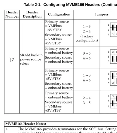
Table 2-1. ConÞguring MVME166 Headers...2-5
Table 2-2. ConÞguring MVME167 Headers...2-8
Table 2-3. ConÞguring MVME177 Headers...2-12
Table 2-4. ConÞguring MVME187 Headers...2-16
Table 2-5. MVME176 Headers...2-20
Table 3-1. Local Bus Memory Map...3-4
Table 3-2. I/O Devices Memory Map...3-6
Table 3-3. Cirrus Logic CD2401 Serial Port Memory Map...3-9
Table 3-4. MC68230 PI/T Register Map...3-13
Table 3-5. 82596CA Ethernet LAN Memory Map...3-14
Table 3-6. 53C710 SCSI Memory Map...3-15
Table 3-7. DS1643/MK48T18 BBRAM/TOD Clock Memory Map...3-16
Table 3-8. BBRAM ConÞguration Area Memory Map...3-17
Table 3-9. TOD Clock Memory Map...3-20
Table 4-1. VMEchip2 Memory Map - LCSR Summary (Sheet 1 of 2)...4-22
Table 4-2. VMEchip2 Memory Map - LCSR Summary (Sheet 2 of 2)...4-24
Table 4-3. DMAC Command Table Format...4-53
Table 4-4. Local Bus Interrupter Summary...4-78
Table 4-5. VMEchip2 Memory Map (GCSR Summary)... 4-110
Table 5-1. Local Bus Transfer Size...5-7
Table 5-2. VSBchip2 Local Control and Status Registers Memory Map...5-21
Table 5-3. VSBchip2 Board Control and Status Registers Memory Map....5-50
Table 6-1. PCCchip2 Devices Memory Map...6-12
Table 6-2. PCCchip2 Memory Map - Control and Status Registers...6-14
Table 7-1. MEMC040 Performance SpeciÞcations...7-3
Table 7-2. MEMC040 Internal Register Memory Map...7-6
Table 8-1. MCECC Performance SpeciÞcations...8-3
Table 8-2. MCECC Internal Register Memory Map, Part 1... 8-11
1
1
Programming Issues
Introduction
The Single Board Computers are complex boards that interface to the VMEbus, VSB, and SCSI bus. These multiple bus interfaces raise the issue of cache coherency and support of indivisible cycles. There are also many sources of bus error. This chapter discusses these topics in addition to the programming interface to each device on the SBC, interrupt handling, and the use of bus timers.
Chapter 2 describes the configurable features of the Single Board Computers.
Chapter 3 describes memory maps for the local devices.
Specific programming information, including information on the programmable registers, is provided for the Application-Specific Integrated Circuit (ASIC) devices in the chapter dedicated to the ASIC, as follows:
Chapter 9 contains diagrams showing connections between the Single Board ComputersÕ printer and serial ports and the MVME712x transition boards.
Programming Interfaces
The next sections describe the programming interface to features of the Single Board Computers. Unless the section calls out a specific Single Board Computer, the discussion applies to all Single Board
Chapter 4 VMEchip2
Chapter 5 VSBchip2
Chapter 6 PCCchip2
Chapter 7 MEMC040 memory controller
Programming Issues
1
MC68040 MPU
The MC68040 processor is used on the MVME166/167. The MC68040 has on-chip instruction and data caches and a floating point processor. Refer to the M68040 user's manual for more information.
MC68060 MPU
The MC68060 processor is used on the MVME176/177. The MC68060 has on-chip instruction and data caches and a floating point processor. Refer to the M68060 user's manual for more information.
M88000 MPU
The MVME187 is based on the M88000 family and uses one MC88100 MPU and two MC88200 or MC88204 CMMUs. One CMMU is used for the data cache and one is used for the instruction cache. Refer to the MC88100 and MC88200 user's manuals for more information.
Data Bus Structure
The Local Bus for all Single Board Computers described in this manual is a 32-bit synchronous bus, which is based on an MC68040-compatible bus and which supports burst transfers. Throughout this manual this bus is referred to as the Local Bus. The various Local Bus master and slave devices use the Local Bus to
communicate. The Local Bus is arbitrated by priority type arbiter. The priority of the Local Bus masters from highest to lowest is:
Highest priority 82596CA LAN
CD2401 serial (through the PCCchip2) 53C710 SCSI
VSB (MVME166/176 only) VMEbus
Programming Interfaces
1
In the general case, any master can access any slave; however, not all combinations pass the common sense test. Refer to the specific section of this manual and to the user's guide for each device to determine its port size, data bus connection, and any restrictions that apply when accessing the device.
EPROMs on the MVME167/176/177/187
All models except the MVME166 include 44-pin PLCC/CLCC EPROM sockets for EPROMs, as follows:
The EPROM sockets support 64K x 16, 128K x 16, and 256K x 16 devices. Many devices may be used, including 27C102JK, 27C202JK, M27C4002, or 27C4096.
The EPROMs are organized as 32-bit wide banks that support 8-, 16-, and 32-bit read accesses. (The MVME166 has Flash memories; the MVME176/177 has Flash memories in addition to the EPROM.)
MVME167 and MVME187
The EPROMs are mapped to Local Bus address 0 following a Local Bus reset. This allows the MC68040 to access the stack pointer and execution address following a reset. It also allows the MC88100 to start executing code at address 0 following a reset. The EPROMs are controlled by the VMEchip2. The map decoder, access time, and when they appear at address 0, is programmable. Refer to the chapter VMEchip2 for more detail.
MVME176/177
The EPROMs on the MVME176/177 share 2MB of memory with the first 2MB of Flash memory. The EPROM can co-exist with 2MB of
Model Sockets Banks
MVME167, 187 4 2
Programming Issues
1
EPROM is writable. Its contents are duplicated in the second 1MB section, which can be read but not written to. The Flash and EPROM configuration is controlled by a jumper as described in Chapter 2, Hardware Configuration, and GPIO bit 2, as described in the chapter VMEchip2.
The EPROMs are mapped to Local Bus address 0 following a Local Bus reset.This allows the MC68060 to access the reset vector and execution address following a reset.
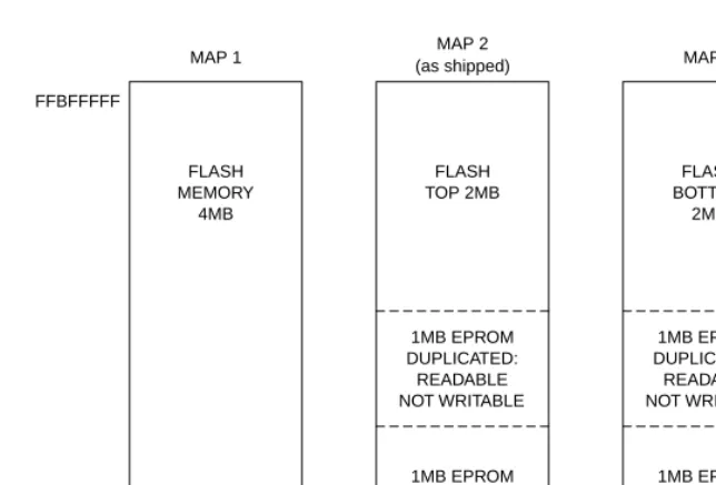
Flash Memory on the MVME176/177
The MVME176/177 includes four 28F008SA Flash memory devices. The 32-bit wide Flash can support 8-, 16-, and 32-bit accesses.The Flash can be used for the onboard debugger firmware, which can be downloaded from I/O resources such as Ethernet, SCSI, serial port, or VMEbus. Flash write-protection is programmable by setting the control bit (GPIO bit 1) in the VMEchip2 GPIO register after downloading.
When the Flash memory is used with EPROM, only the top or bottom 2MB of Flash memory is visible at any one time. For accessing the shadowed area of Flash, the 176/177Bug provides the
SFLASH command.
The MVME176/177 is shipped with the top 2MB of Flash memory and EPROM mapped as illustrated by Map 2 in Figure 1-1.
The 176/177Bug is shipped in EPROM. To map all 4MB of Flash and retain access to the 176/177Bug, perform the following steps:
1. Map Flash and EPROM as shown in Map 3 in Figure 1-1.
2. Copy the 176/177Bug into the bottom 2MB of Flash memory.
Programming Interfaces
1
Figure 1-1. MVME176/177 Flash and EPROM Memory Mapping Schemes
Flash Memory and Download EPROM on the MVME166
The MVME166 includes four 28F020 Flash memory devices and a download EPROM. These parts replace the four EPROM sockets used on the MVME167/187. The Flash parts are programmable on the MVME166 board and the programming code is provided in the download EPROM. The Flash devices provide 1MB of ROM. The download EPROM provides 128KB of ROM. The download EPROM is mapped to Local Bus address 0 following a Local Bus reset. This allows the MC68040 to access the stack pointer and execution address following a reset. The download EPROM appears at 0 until the DR0 bit is cleared in the PCCchip2 chip. The Flash devices are controlled by the VMEchip2 and the download EPROM is controlled by the PCCchip2. The PC0 bit in the MC68230 FFBFFFFF
FF800000
MAP 1 (as shipped)MAP 2 MAP 3
FLASH MEMORY
4MB
FLASH BOTTOM
2MB
FFBFFFFF
FLASH TOP 2MB
1MB EPROM DUPLICATED: READABLE NOT WRITABLE
1MB EPROM DUPLICATED:
READABLE NOT WRITABLE
1MB EPROM (BUG)
1MB EPROM
FF800000 FFA00000
FF900000
1534 9408
Programming Issues
1
The EPROM contains the BootBug product (166BBug). Because Flash memory can be electronically erased, the EPROM firmware is a subset of the regular debugger product. It contains enough functionality from the debugger to permit downloading of object code (via VMEbus, serial port, SCSI bus, or the network) and reprogramming of the Flash memory.
A jumper on the MVME166 (J3, pins 7 and 8) controls the operation of the BootBug:
❏ If the jumper is in place, the BootBug (which always executes
at power-up and reset) passes execution to the full debugger contained in Flash memory.
❏ If the jumper is removed, execution continues (with
diminished functionality) in the BootBug.
Before you perform any SCSI, VMEbus, or Ethernet I/O with the MVME166, it may be necessary to define some parameters (e.g., SCSI ID, Ethernet address, VMEbus mapping). For details on configuring the MVME166, refer to the setup command description in the MVME167Bug Debugging Package User's Manual.
SRAM
The Single Board Computers include 128KB of 32-bit wide static RAM that supports 8-, 16-, and 32-bit wide accesses. The SRAM allows the debugger to operate and limited diagnostics to be executed without the DRAM mezzanine. The SRAM is controlled by the VMEchip2, and the access time is programmable. Refer to the chapter VMEchip2 for more detail. The boards are populated with 100 ns SRAMs.
The Single Board Computers provide for battery backup for the SRAM. (The backup circuitry is standard on the
Programming Interfaces
1
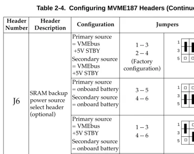
The MVME166 and MVME187 implementations support primary and secondary back up power sources. The boards include jumpers that allow the power inputs of the DS1210S to be connected to either the VMEbus +5 V STDBY pin or to one cell of the onboard battery. For example, the primary backup source may be from the VMEbus +5 V STDBY pin and the secondary source may be the onboard battery.
The MVME167 and MVME176/177 implement a single backup source. You can select one of the following: +5V standby, the onboard battery, or no backup power.
The jumpers for each board are described in the chapter Hardware Configuration.
Onboard DRAM
The DRAM map decoder can be programmed to accommodate different base address(es) and sizes of mezzanine boards. The onboard DRAM is disabled by a Local Bus reset and must be programmed before the DRAM can be accessed.
Most DRAM devices require some number of access cycles before the DRAMs are fully operational. Normally this requirement is met by the onboard refresh circuitry and normal DRAM initialization. However, software should insure a minimum of 10 initialization cycles are performed to each bank of RAM.
Detailed programming information is available in the chapters on the memory options.
Battery Backed Up RAM and Clock
Programming Issues
1
VMEbus Interface
The Local Bus to VMEbus interface, the VMEbus to Local Bus interface, and the local-VMEbus DMA controller functions are provided by the VMEchip2. The VMEchip2 can also provide the VMEbus system controller functions. Refer to the chapter VMEchip2, for detailed programming information.
VME Subsystem Bus (VSB) Interface
The Local Bus to VSB interface and the VSB to Local Bus interface are provided by the VSBchip2, only on the MVME166/176 board. The VSB uses the P2 connector of the MVME166/176. Refer to the chapter VSBchip2 for detailed programming information for the VSBchip2.
I/O Interfaces
The Single Board Computers provides onboard I/O for many system applications. The I/O functions include serial ports, parallel (printer) port, Ethernet transceiver interface, and SCSI mass storage interface.
Serial Port Interface
The CD2401 serial controller chip (SCC) is used to implement the serial ports. On all Single Board Computers, the interface provided by the PCCchip2 allows the 16-bit CD2401 to appear at contiguous addresses; however, accesses to the CD2401 must be 8 or 16 bits; 32-bit accesses are not permitted. Refer to the CD2401 data sheet and to the chapter PCCchip2 for detailed programming information.
Programming Interfaces
1
The next subsections describe the two implementations of the serial ports.
Serial Port Interface (MVME167/177/187)
The four serial ports support the standard baud rates (110 to 38.4K baud). The serial ports are different functionally because of the limited number of pins on the P2 I/O connector:
❏ Serial port 1 is a minimum function asynchronous port. It
uses RXD, CTS, TXD, and RTS.
❏ Serial ports 2 and 3 are full function asynchronous ports.
They use RXD, CTS, DCD, TXD, RTS, and DTR.
❏ Serial port 4 is a full function asynchronous or synchronous
port. It can operate at synchronous bit rates up to 64 k bits per second. It uses RXD, CTS, DCD, TXD, RTS, and DTR. It also interfaces to the synchronous clock signal lines. Refer to the chapter Printer and Serial Port Connections for drawings of the serial port interface connections.
All four of these serial ports use EIA-232-D drivers and receivers located on the main board, and all the signal lines are routed to the I/O connector. The configuration headers are located on the main board and the MVME712seriestransition board. An external I/O transition board such as the MVME712x should be used to provide configuration headers and industry-standard connectors.
Programming Issues
1
Serial Port Interface (MVME166/176 Only)
The four serial ports on the MVME166/176 are functionally the same. All serial ports are full function asynchronous or
synchronous ports. They can operate at synchronous bit rates up to 64 k bits per second. They use RXD, CTS, DCD, TXD, RTS, DTR, and DSR. They also interface to the synchronous clock signal lines.
Additional control signals are provided for each serial port by the MC68230 Parallel Interface/Timer. These include local loopback control, self test control, and ring indicator. The ring indicator signal can be programmed to generate a Local Bus interrupt. Refer to the MC68230 section for additional information. Refer to chapter 9 for drawings of the serial port interface connections. Note that the usable functionality of the serial ports depends on the transition module used.
All four serial ports use a TTL interface to the transition board. This allows the interface specific drivers to be located on the transition board. This allows more flexibility in configuring the serial ports for different interfaces like EIA-232-D or V.35. An external I/O transition module such as the MVME712-10 should be used to provide configuration headers, interface drivers, and industry-standard connectors.
MC68230 Parallel Interface/Timer (MVME166/176 Only)
The MVME166/176 provides an MC68230 parallel interface/timer (PI/T) chip. When the MVME166/176 is used with the MVME712-10 transition module or the MVME712-06/07/09 I/O distribution board set, the MC68230 is used to provide additional control lines for the serial ports. These include local loopback, self test, and ring indicator. The ring indicator signals can be programmed to
generate Local Bus interrupts. Refer to the chapter Printer and Serial Port Connections in this manual, and to the MVME712-10 transition module manual, for more information.
The base address of the MC68230 is $FFF45E00, and because it is an 8-bit device it appears only at odd addresses. Space for the
Programming Interfaces
1
copies of the CD2401 registers into eight segments. The CD2401 is still addressed at $FFF45000 to $FFF451FF. Addresses $FFF45200 to $FFF45BFF are reserved, and if accessed on an MVME166/176 cause a Local Bus time-out error, if the Local Bus timer is enabled. The address range from $FFF45C00 to $FFF45DFF always returns a Local Bus time-out error if the Local Bus timer is enabled. The CD2401 appears redundantly from $FFF45200 to $FFF45FFF on the MVME167/177/187.
The presence of the MC68230 can be determined by reading address $FFF45C00. If a time-out error occurs, then the board is an MVME166/176 and the MC68230 is present. If a time-out does not occur, then the board is an MVME167/177/187 and the MC68230 is not present. The Local Bus time-out timer in the VMEchip2 must be enabled for this test.
Programming Issues
1
Parallel (Printer) Interface
All models have a parallel (printer) interface. The interface is provided by the PCCchip2. Refer to the chapter PCCchip2 for detailed programming information. Refer to the chapter Printer and Serial Port Connections for drawings of the printer port interface connections.
Ethernet Interface
The 82596CA is used to implement the Ethernet transceiver interface. The 82596CA accesses local RAM using DMA operations to perform its normal functions. Because the 82596CA has small internal buffers and the VMEbus has an undefined latency period, buffer overrun may occur if the DMA is programmed to access the VMEbus or VSB. Therefore, the 82596CA should not be
programmed to access the VMEbus or VSB.
Each Single Board Computer is assigned an Ethernet Station Address. The address is $08003E2xxxxx where xxxxx is the unique 5-nibble number assigned to a board.
Each board has an Ethernet Station Address displayed on a label attached to the VMEbus P2 connector. In addition, the six bytes including the Ethernet address are stored in the configuration area of the BBRAM. That is, 08003E2xxxxx is stored in the BBRAM. At an address of $FFFC1F2C, the upper four bytes (08003E2x) can be read. At an address of $FFFC1F30, the lower two bytes (xxxx) can be read. Refer to the BBRAM, TOD Clock memory map description in the chapter Memory Maps. The MVME166 BootBug has the capability to retrieve or set the Ethernet address, as do the other Single Board Computer debuggers.
If the data in the BBRAM is lost, use the number on the VMEbus P2 connector label to restore it.
Programming Interfaces
1
Support functions for the 82596CA are provided by the PCCchip2. Refer to the 82596CA user's guide and to the chapter PCCchip2 for detailed programming information.
SCSI Interface
The Single Board Computers provide for mass storage subsystems through the industry-standard SCSI bus. These subsystems may include hard and floppy disk drives, streaming tape drives, and other mass storage devices. The SCSI interface is implemented using the NCR 53C710 SCSI I/O controller.
Support functions for the 53C710 are provided by the PCCchip2. Refer to the 53C710 user's guide and to the chapter PCCchip2 for detailed programming information.
SCSI Termination
The system configurer must ensure that the SCSI bus is properly terminated at both ends. This is done on each system as follows:
MVME167 MVME177 MVME187
Sockets are provided for the terminators on the P2 transition board. If the SCSI bus ends at the P2 transition board, then termination resistors must be installed on the P2 transition board. +5V power to the SCSI bus TERM power line and termination resistors is provided through a fuse located on the P2 transition board (for the MVME167 and MVME187), but is provided through a fuse on the MVME712 transition board and a diode on the P2 transition board (for the MVME177).
MVME166 MVME176
Programming Issues
1
Local Resources
The Single Board Computers include many resources for the local processor. These include tick timers, software programmable hardware interrupts, watchdog timer, and Local Bus time-out.
Programmable Tick Timers
Four 32-bit programmable tick timers with 1 µsec resolution are provided, two in the VMEchip2 and two in the PCCchip2. The tick timers can be programmed to generate periodic interrupts to the processor. Refer to the chapters VMEchip2 and PCCchip2,
respectively, for detailed programming information.
Watchdog Timer
A watchdog timer function is provided in the VMEchip2. When the watchdog timer is enabled, it must be reset by software within the programmed time or it times out. The watchdog timer can be programmed to generate a SYSRESET signal, local reset signal, or board fail signal if it times out. Refer to the chapter VMEchip2 for detailed programming information.
Software-Programmable Hardware Interrupts
Eight software-programmable hardware interrupts are provided by the VMEchip2. These interrupts allow software to create a hardware interrupt. Refer to the chapter VMEchip2 for detailed programming information.
Local Bus Time-out
Interrupt Handling
1
VMEbus bound cycles are timed by the VMEbus access timer and the VMEbus global timer. Refer to the chapter VMEchip2 for detailed programming information.
VSB bound cycles are timed by the VSB access timer, the VSB transfer timer, and if its serial arbiter is enabled, by the VSB arbitration timer. Refer to the chapter VSBchip2 for detailed programming information.
Interrupt Handling
Because the M68000-based systems use hardware-vectored interrupts while the MC88100 does not, interrupts are handled differently on the Single Board Computers based on those
processors. The C040 bit in the PCCchip2 General Control Register (address $FFF42002) should be set when the board MPU is from the M68000 family. It should be cleared when the MPU is an MC88100. For more information, refer to ÒInterrupt PrioritizerÓ (MVME187) in the chapter PCCchip2.
Most interrupt sources are level and base vector programmable. Interrupt vectors from the PCCchip2, VSBchip2, and the VMEchip2 have two sections:
There is an onboard daisy chain of interrupt sources, prioritized as follows:
Base value Can be set by the processor, usually the upper
four bits
Lower bits Set according to the particular interrupt source
Highest priority Interrupts from the PCCchip2
Next Interrupt sources from the VSBchip2
Programming Issues
1
The interrupt scheme varies according to the processor:
The Local Bus distinguishes interrupt acknowledge cycles from other cycles by placing the binary value %11 on TT1-TT0. It also specifies the level that is being acknowledged using TM2-TM0. The interrupt handler selects which device within that level is being acknowledged.
Interrupt Programming Examples
This section demonstrates how to use interrupts on Single Board Computers.
Read this entire section before performing any of these procedures.
The first subsection gives an example of how to generate and handle a VMEchip2 Tick Timer 1 interrupt on M68000-based Single Board Computers. Specific values have been given for the register writes.
The second subsection talks about how interrupts are handled on the MVME187. There are substantial differences in the way interrupts are handled on the MVME187 and the M68000-based Single Board Computers.
MC68040 mode Seven-level prioritized, hardware-vectored
interrupt scheme that is standard in the M68000 family
MC88100 mode All interrupt sources are combined into one
Interrupt Handling
1
M68000 VMEchip2 Tick Timer 1 Periodic Interrupt Example
A. Set up Tick Timer 1.
Step Register Address Action and Reference
1. Prescaler Control
Register
$FFF4004C If not already initialized by the debugger, initialize as follows: Prescaler Register = 256 - Bclock (MHz). This gives a 1 MHz clock to the tick timers. Bclock is the bus clock rate, such as 25 MHz. 256 - 25 = $E7.
2. Tick Timer 1
Compare Register
$FFF40050 For periodic interrupts, set the Compare Register value = Period (µs). For example, if you want an interrupt every millisecond, set the register value to 1000 ($3E8). Refer to the Tick Timer 1 Compare Register
description in the chapter
VMEchip2.
3. Tick Timer 1 Counter
Register
$FFF40054 Write a 0 to clear.
4. Tick Timer 1 Control
Register
$FFF40060 (8 bits)
Programming Issues
1
B. Set up the Local Bus interrupter:
Periodic Tick Timer 1 interrupts now occur, so you need an interrupt handler. Section C gives the details, as follows.
Step Register Address Action and Reference
5. Vector Base Register $FFF40088
(8 of 32 bits)
If not already initialized by the debugger, set interrupt base register 0 by writing to bits 28-31. Refer to the Vector Base Register description and to Table 4-4, Local Bus Interrupter Summary, in the chapter
VMEchip2.
6. Interrupt Level
Register 1 (bits 0-7)
$FFF40078 (8 of 32 bits)
Write desired level of Tick Timer 1 interrupt to bits 0-2.
7. Local Bus Interrupter
Enable Register
$FFF4006C (8 of 32 bits)
Set bit 24 (ETIC1) to 1 to enable Tick Timer 1 interrupts.
8. I/O Control Register
1
$FFF40088 (8 of 32 bits)
Write a 1 to bit 23 to enable interrupts from the
VMEchip2. A zero masks all
Interrupt Handling
1
C. How to set up an interrupt handler routine. (Your interrupt handler should include the following features.)
MVME187 Interrupt Handling
The M88000 architecture currently does not support prioritized interrupts like the M68000 family. A single interrupt request is connected to the MC88100, and all device interrupt requests are summed into this signal. Software prioritization is required to implement interrupt priority encoding. Logic on the MVME187 assists the 88K software by encoding the interrupt priority in hardware.
A summary of the interrupt handling protocol for the MVME187 follows. Step numbers refer to circled items on Figure 1-2, which illustrates the protocol.
Step Action and Reference
1. Be sure the M68000 vector base register is set up. Set the proper M68000 exception vector location so the processor vectors to your interrupt handler location. You can determine proper exception vector location to set from the M68000 vector base register, the VMEchip2 base register, and Table 4-4, Local Bus Interrupter Summary, from which you can determine the actual interrupt vector given on a Tick Timer 1 interrupt. Lower the M68000 mask so the vector level you programmed is accepted. The interrupt handler itself should include the following (steps 2 through 5).
2. ConÞrm the Tick Timer 1 interrupt occurred, by reading the status of bit 24 of the Interrupter Status Register at $FFF40068. A high indicates an interrupt present.
3. Clear Tick Timer 1 interrupt by writing a one to bit 24 of the Interrupt Clear Register at $FFF40074.
4. Increment a software counter to keep track of the number of
interrupts, if desired. Output a character or some other action (such as toggling the FAIL LED) on an appropriate count, such as 1000.
Programming Issues
1
Step Action and Reference
1. A device requests interrupt service from the MPU. The hardware logic
on the MVME187 PCCchip2 encodes this request on the INT signal connected to the MC88100. INT is asserted if the following is true:
a. PCCchip2 Master Interrupt Enable is on, and
b. External (Device) Interrupt Request Level is greater than the Interrupt Mask Level Register and greater than 0.
2. The MC88100 saves its current context in order to service the interrupt request. The M88000 architecture requires that nested exceptions be handled totally in software. The MVME187 logic provides an external prioritizer for the hardware interrupts to assist in nested interrupt architecture.
Software applications (operating systems, etc.) are encouraged to take advantage of the interrupt prioritizer. An example of how to use the prioritizer is given in the following steps.
After the context of the processor is saved, the MC88100 is able to mask out interrupts with priorities lower than the current request under service. This masking operation is optional but recommended.
3. The MC88100 then (through the Data CMMU) reads the Interrupt
Priority Level Register on the PCCchip2 to determine the priority level of the interrupt request. At this time, the priority level is determined and the corresponding interrupt mask may be written to the PCCchip2, which masks any interrupts of equal or lower priority. This masking allows the application software (or operating system) to unfreeze shadowing and quickly re-enable exception handling. Without the Interrupt Mask Level Register and its associated interrupt prioritization, interrupt prioritization would have to be handled totally through software.
Interrupt Handling
1
5. The IACK cycle causes a ÒvectorÓ to be passed to the Data
CMMU/MC88100 that can be used to index a table of interrupt service routine pointers. The initialization of the MVME187 module determines the interrupt priority and the device interrupt vectors, relieving
considerable software overhead to determine interrupt priority.
Cache Coherency
1
Cache Coherency
The next subsections describe the way each processor manages cache coherency.
Cache Coherency, MVME166/167
The MC68040 has the ability to watch Local Bus cycles executed by other Local Bus masters such as the SCSI DMA controller, the LAN, the VMEchip2 DMA controller, the VMEbus to Local Bus
controller, and the VSB to Local Bus controller. This bus snooping capability is described in the M68040 Microprocessors UserÕs Manual sections on Cache Coherency and Bus Snooping Operation.
When snooping is enabled, the MC68040 MPU can source data and invalidate cache entries as required by the current cycle. The MPU cannot watch VMEbus or VSB cycles that do not access the Local Bus. Software must ensure that data shared by multiple processors is kept in un-cached memory. The software must also mark all onboard I/O areas as cache inhibited and serialized.
Cache Coherency, MVME176/177
The MC68060 has the ability to watch the external bus during accesses by other bus masters, maintaining coherency between the MC68060Õs caches and external memory systems.To maintain cache coherency, the MC68060 provides automatic snoop-invalidation when it is not the bus master. When an external cycle is marked as snoopable, the bus snooper checks the caches and invalidates the matching data.
Unlike the MC68040, the MC68060 cannot source or sink cache data during alternate bus master accesses. Therefore, the MVME176/177 uses a single snoop control line Ð SC1. Snoop control bits for SC0 must be set to 0.
Programming Issues
1
Cache Coherency, MVME187
Snooping is not supported on the MVME187. Software must ensure that data shared by multiple processorsis kept in un-cached memory. The software must also mark all onboard I/O areas as cache inhibited and serialized. Snoop control bits in the 53C710, VMEchip2, VSBchip2, and PCCchip2 must be set to 0 (snoop disabled).
Using Bus Timers
This section illustrates the use of bus timers by describing the sequence of events when the MPU on one Single Board Computer accesses the Local Bus memory on another Single Board Computer using the VMEbus. A similar sequence of events could be described if the access occurred over the VSB. This scenario involves three bus timers, which normally should be set to quite different values:
The sequence begins when the MPU asserts a request for the Local Bus. The MPU must wait until the Local Bus is released by the current bus master before its cycle can begin. When the MPU is granted the Local Bus, it begins its cycle and the Local Bus timer starts counting. It continues to count until an address decode of the VMEbus address space is detected and then the timer stops. This is normally a very short period of time. In fact, all Local Bus non-error bus accesses are normally very short, such as the time to access onboard memory. Therefore, it is recommended this timer be set to a small value, such as 8 µsec.
Local bus timer Measures the time an access to an onboard resource takes
VMEbus access timer
Measures the time from when the VMEbus request has been initiated to when a VMEbus grant has been obtained
Global VMEbus timer
Using Bus Timers
1
The next timer to take over when one Single Board Computer accesses another is the VMEbus access timer. This measures the time between when the VMEbus has been address decoded and hence a VMEbus request has been made, and when VMEbus mastership has been granted. Because we have found in the past that some VME systems can become very busy, we recommend this time-out be set at a large value, such as 32 msec. For debug
purposes this value can also be set to infinity.
Once the VMEbus has been granted, a third timer takes over. This is the global VMEbus timer. This timer starts when a transfer actually begins (DS0 or DS1 goes active) and ends when that transfer completes (DS0 or DS1 goes inactive). This time should be longer than any expected legitimate transfer time on the bus. We normally set it to 256 µsec. This timer can also be disabled for debug purposes.
Before a Single Board Computer access to another Single Board Computer can complete, however, the VMEchip2 on the accessed board must decode a slave access and request the Local Bus of the second board. When the Local Bus is granted (any in-process onboard transfers have completed), then the Local Bus timer of the accessed board starts. Normally, this is also set to 8 µsec. When the memory has the data available, a transfer acknowledge signal (TA) is given. This translates into a DTACK signal on the VMEbus which is then translated into a TA signal to the first requesting processor, and the transfer is complete.
Programming Issues
1
Indivisible Cycles
The Single Board Computers perform operations that require indivisible read-modify-write (RMW) memory accesses. These RMW sequences occur when the MMU modifies table entries or when the MPU executes one of the single-cycle instructions listed in Table 1-1.
Note Software emulation of CAS2 and misaligned CAS instructions is performed by the MC68060 Software Package, which is included in all Motorola-supplied operating systems for the MVME176/177. Contact your sales office for information about obtaining the MC68060 Software Package for use with other operating systems.
The Single Board Computers do not fully support all RMW operations in all possible cases. The modules make the following assumptions and support a limited subset of RMW instructions:
❏ The Single Board Computers support single-address RMW
cycles.
❏ Multiple-address RMW cycles are not guaranteed indivisible
and may cause illegal VMEbus cycles.
Table 1-1. Single-Cycle Instructions
MPU Instructions
MC68040 CAS, CAS2, TAS
MC68060 CAS
CAS2 and misaligned CAS instructions are emulated by software (see NOTE)
No Supervisor Stack Pointer on MC68060
1
❏ Lock cycles caused by MMU table walks on the VMEbus do
not cause illegal VMEbus cycles but they are not guaranteed do be indivisible.
On M68000-based systems, aligned CAS and all TAS cycles are always single-address RMW operations, while misaligned CAS and CAS2 operations and operations in the MMU can be address RMW cycles. The VMEbus does not support multiple-address RMW cycles and there is no defined protocol for
supporting multiple-address RMW cycles that start onboard and then access offboard resources. Because it is not possible to tell if the processor is executing a single- or multiple-address read-modify-write cycle, software should only execute single-address RMW instructions. For efficiency, all CAS instructions should be aligned.
No Supervisor Stack Pointer on MC68060
On the MC68060, use of the supervisor stack pointer is reserved for system programming functions. All application software must be written to run in user mode. Such software will migrate to any M68000 platform without modification.
Programs that were written for platforms like the MC68040 that use the supervisor stack pointer must be recompiled before you can run them on an MC68060-based Single Board Computer, such as the MVME176/177.
Sources of Local BERR*
A TEA* signal (indicating a bus error) is returned to the Local Bus master when a Local Bus time-out occurs, a DRAM parity error occurs and parity checking is enabled, or a VME bus error occurs during a VMEbus access.
Programming Issues
1
Local Bus Time-out
A Local Bus Time-out occurs whenever a Local Bus cycle does not complete within the programmed time (VMEbus bound cycles are not timed by the Local Bus timer). If the system is configured properly, this should only happen if software accesses a non-existent location within the onboard address range.
VMEbus Access Time-out
A VMEbus Access Time-out occurs whenever a VMEbus bound transfer does not receive a VMEbus bus grant within the
programmed time. This is usually caused by another bus master holding the bus for an excessive period of time.
VMEbus BERR*
A VMEbus BERR* occurs when the BERR* signal line is asserted on the VMEbus while a Local Bus master is accessing the VMEbus. VMEbus BERR* should occur only if: an initialization routine samples to see if a device is present on the VMEbus and it is not, software accesses a non-existent device within the VMEbus range, incorrect configuration information causes the VMEchip2 to incorrectly access a device on the VMEbus (such as driving LWORD* low to a 16-bit board), a hardware error occurs on the VMEbus, or a VMEbus slave reports an access error (such as parity error).
Local DRAM Parity Error
When parity checking is enabled, the current bus master receives a bus error if it is accessing the local DRAM and a parity error occurs.
VMEchip2
Error Conditions
1
VSBchip2 BERR*
The VSBchip2 on the MVME166/176 will return TEA* when specific VSB errors occur. Refer to the chapter VSBchip2 for more information on bus errors from the VSB.
Bus Error Processing
Because different conditions can cause bus error exceptions, the software must be able to distinguish the source. To aid in this, status registers are provided for every Local Bus master. The next section describes the various causes of bus error and the associated status registers.
Generally, the bus error handler can interrogate the status bits and proceed with the result. However, an interrupt can happen during the execution of the bus error handler (before an instruction can write to the status register to raise the interrupt mask). If the interrupt service routine causes a second bus error, the status that indicates the source of the first bus error may be lost. The software must be written to deal with this.
Error Conditions
This section lists the various error conditions that are reported by the Single Board Computer hardware. A subheading identifies each error condition; a standard format provides the following
information:
❏ Description of the error
❏ How notification of the error is made
Programming Issues
1
MPU Parity Error
MPU Offboard Error
MPU TEA - Cause Unidentified
Description: A DRAM parity error.
MPU NotiÞcation: TEA is asserted during an MPU DRAM access.
Status: Bit 9 of the MPU Status and DMA Interrupt Count
Register in the VMEchip2 at address $FFF40048.
Comments: After memory has been initialized, this error
normally indicates a hardware problem.
Description: An error occurred while the MPU was attempting to
access an offboard resource.
MPU NotiÞcation: TEA is asserted during offboard access.
Status: Bit 8 of the MPU Status and DMA Interrupt Count
Register.
Address $FFF40048
Comments: This can be caused by a VMEbus time-out, a VMEbus
BERR, or a Single Board Computer VMEbus access time-out. The l