University of Windsor University of Windsor
Scholarship at UWindsor
Scholarship at UWindsor
Electronic Theses and Dissertations Theses, Dissertations, and Major Papers
2009
A Non-planar CMUT Array for Automotive Blind Spot Detection
A Non-planar CMUT Array for Automotive Blind Spot Detection
Syed Abbas
University of Windsor
Follow this and additional works at: https://scholar.uwindsor.ca/etd
Recommended Citation Recommended Citation
Abbas, Syed, "A Non-planar CMUT Array for Automotive Blind Spot Detection" (2009). Electronic Theses and Dissertations. 113.
https://scholar.uwindsor.ca/etd/113
A Non-planar CMUT Array for
Automotive
Blind Spot Detection
by
Syed Yasir Abbas
A Thesis
Submitted to the Faculty of Graduate Studies
through Electrical and Computer Engineering
In Partial Fulfillment of the Requirements
for the Degree of Master of Applied Science
at the University of Windsor
Windsor, Ontario, Canada
Author’s Declaration of Originality
I hereby certify that I am the sole author of this thesis/major paper and that no
part of this thesis/major paper has been published or submitted for publication.
I certify that, to the best of my knowledge, my thesis/major paper does not
infringe upon anyone's copyright nor violate any proprietary rights and that any
ideas, techniques, quotations, or any other material from the work of other people
included in my thesis, published or otherwise, are fully acknowledged in
accordance with the standard referencing practices. Furthermore, to the extent
that I have included copyrighted material that surpasses the bounds of fair
dealing within the meaning of the Canada Copyright Act, I certify that I have
obtained a written permission from the copyright owner(s) to include such
materials in my major paper and have included copies of such copyright
clearances to my appendix.
I declare that this is a true copy of my dissertation, including any final revisions,
as approved by my committee and the Graduate Studies Office, and that this
dissertation has not been submitted for a higher degree to any other University or
Abstract
A discretized hyperbolic paraboloid geometry capacitive micromachined
ultrasonic transducer (CMUT) array has been designed and fabricated for
automotive blind spot monitoring application. The array is designed for a
frequency range of 113-167 kHz, beamwidth of 20±50 with a maximum sidelobe intensity of -6dB. An SOI based fabrication technology has been used for the 5x5
array with 5 sensing surfaces along each x and yaxis and 7 elevation levels. An
assembly and packaging technique has been developed to realize the non-planar
geometry in a PGA-68 package. Two new analytical models has been developed
to more accurately calculate the deflection profile of a thin square membrane and
capacitance change due to both external mechanical pressure and the
electrostatic pressure due to the bias voltage. The developed models incorporate
the effects of bias voltage, external pressure, fringing field capacitance and large
deflections. Both the models exhibit excellent accuracy when compared with
Acknowledgment
At the outset I bow before Almighty GOD, Omnipotent and Omnipresent without whose blessing no human being can do anything. I wish to express my gratitude to those who generously helped me to color the mosaic of this project with tiles of their knowledge, expertise and memory.
I feel great pleasure in expressing my gratitude to my mentor Dr. Sazzadur Chowdhury, who kept full faith in me. His encouraging supervision and assistance in tracking down errors and omissions made it possible for me to finish this work in time.
I would like to express my gratitude to Dr. Raafat Mansour, for allowing me to use the wonderful facility at CIRFE, University of Waterloo. I would also like to thank Mr. Bill Jolley and Mr Siamakh Fouladi for there valuable inputs during my stay at Waterloo. To my lab mate and a wonderful senior colleague, Dr. Md. Mosaddequr Rahman, for his valuable inputs and discussions “☺”.
I would like to thank NSERC and Ontario’s Centre of Excellence (OCE) for their financial support and also Canadian Microelectronic Corporation (CMC) and IntelliSuite™ for there technical support.
Table of Content
Author’s Declaration of Originality iii
Abstract iv
Dedication v
Acknowledgment vi
List of Figures ix
List of Tables xii
Chapter 1: Introduction 1
1.1 Goals 1
1.2 Background 2
1.3 State-of-the-Art 3
1.4 Limitations of the Current Models 4
1.5 Scientific Approach to Solve the Problem 5
1.6 Target Applications 6
1.7 Specific Research Objectives 9
1.8 Principle Results 10
1.9 Organization of Thesis 11
Chapter 2: Micro-Array Theory 13
2.1 Background 13
2.2 Array Geometrical Specification Determination 20
2.2.1 Array Sidelength 20
2.1.2 Number of Sensing Surfaces 21
2.1.3 Array Height 21
3.1 Capacitive Micromachined Ultrasonic Transducers (CMUTs): Operating
Principle 26
3.2 New Analytical Model for Capacitance Change 28
3.2.1 Capacitance Change 28
3.2.2 Electrostatic Pressure 33
3.2.3 Center Deflection 35
3.2.4 Combined Load Deflection Model 36
3.3 CMUT Lumped Element Model 37
3.4 Design Performance and Verification 40
3.5 Beam Shapes 47
Chapter 4: Fabrication 51
4.1 Array Fabrication Details 51
4.2 Fabrication Process 54
Chapter 5: Assembly and Packaging 72
5.1 Assembly Details 72
5.2 Packaging Details 78
Chapter 6: Conclusions and Future Work 84
6.1 Conclusion 84
6.2 Future Work 86
References 87
Appendix A 91
A.1 Center Deflection Vs Biasing Voltage 92
A.2 Capacitance Vs Biasing Voltage 94
List of Figures
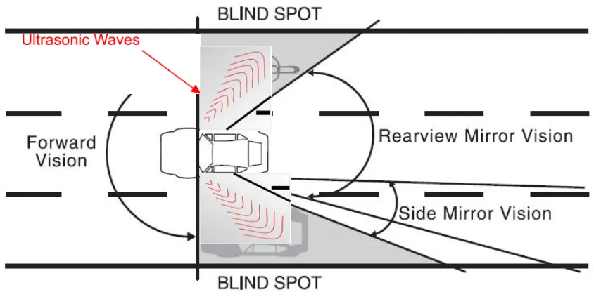
Figure 1.1. Blind Spot Detection Scheme………..(7)
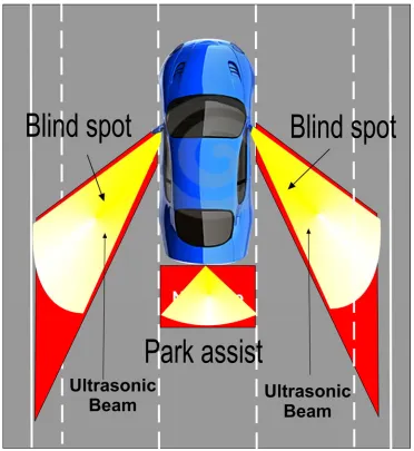
Figure 1.2. Parking Assistance Scheme………(8)
Figure 2.1. Illustration of Synthesis Array Theory……….(15)
Figure 2.2. Hyperbolic Paraboloid (Continuous)……….…(16)
Figure 2.3. Hyperbolic Paraboloid (Out of Plane twist isα)……….….(17)
Figure 2.4. Array Height Sampling ………..(22)
Figure 2.5. Design A (7x7 Array)………..(24)
Figure 2.6. Design B (5x5 Array)………..(25)
Figure 3.1. Basic Structure of a Capacitive Sensor……….…….(27)
Figure 3.2. Electrical Equivalent Circuit Model of a Capacitive Type Acoustical Sensor ……….…..(37)
Figure 3.3. Center Deflection Vs Voltage……….…...(44)
Figure 3.4. Capacitance Vs Voltage……….…(44)
Figure 3.5. Center Deflection Vs Pressure……….….(45)
Figure 3.6. Pull-In Voltage Curve obtained from IntelliSuite™ 3-D TEM ….…..(45)
Figure 3.7. IntelliSuite™ Generated Image of Diaphragm at Pull-In…………...(46)
Figure 3.8. 7x7 Array Beam Shape at 113 kHz………...(47)
Figure 3.9. 7x7 Array Beam Shape at 140 kHz……….….(48)
Figure 3.13. 5x5 Array Beam Shape at 167 kHz………...….…………(50)
Figure 4.1. Fabrication Material Legend. ……….……...(52)
Figure 4.2(a). Step 1 Conceptual cross-section. ………...(54)
Figure 4.2(b). Step 1 IntelliSuiteTM generated 3-D model. ………...(54)
Figure 4.2 (c). Actual Picture taken during and after the RCA clean fabrication process steps respectively. ………...(55)
Figure 4.3(a). Step 2 Conceptual cross-section……….(56)
Figure 4.3(b). Step 2 IntelliSuiteTM generated 3-D model. ………...(56)
Figure 4.3(c). Actual Picture taken before and after Metallization…………..….(57)
Figure 4.4(a). Single Sensing Surface Details (Conceptual) ………...(60)
Figure 4.4(b). Complete Mask Details. ………...(61)
Figure 4.4(c). Images after Photolithography. ………...(62)
Figure 4.4(d). Optical Profiler Images (Etch Hole Dimension). ………..(63)
Figure 4.4(e). Optical Profiler Images (Etch Hole Separation). ………..(64)
Figure 4.5(a). Step 4 Conceptual cross-section……….(65)
Figure 4.5(b). Step 4IntelliSuiteTM generated 3-D model………..(65)
Figure 4.5(c). Actual Picture taken after Metal Etch………..(65)
Figure 4.6(a). Step 5 Conceptual cross-section……….(66)
Figure 4.6(b). Step 5 IntelliSuiteTM generated 3-D model. ………...(66)
Figure 4.6(c). Optical Profiler Images after Silicon Etch (RIE) ………(67)
Figure 4.8(b). Step 7 IntelliSuiteTM generated 3-D model……….…(71)
Figure 4.8(c). Actual Image after release. ……….….(71)
Figure 5.1(a). Illustration of Short Circuit Condition………..…(74)
Figure 5.1(b). Illustration After Non-Conductive Vertical Coating……….….….(74)
Figure 5.1(c). Illustration of Silicon Shim Wafer Inside a PGA-68. ………..…..(75)
Figure 5.1(d). Illustration of sensing surface over silicon shim wafer (Side
view).……….……….(76)
Figure 5.1(e). Illustration of sensing surface over silicon shim wafer (Top
view).………..…………(77)
Figure 5.2(a). Top View of PGA-68 Package……….………...(79)
Figure 5.2(b). Bottom View of PGA-68 Package. ………....(79)
Figure 5.3. 5x5 Array Pin Connection Scheme (PGA-68 Package)…………..(81)
Figure 5.4. Complete 5x5 Array (Top view)………...(82)
List of Tables
Table 2.1. Beamwidth Control Parameter K Value…..………(20)
Table 2.2. Array Specification (Design A)……….………..……..(23)
Table 2.3. Array Specification (Design B)…….……….………..….(25)
Table 3.1. Transducer Design Specifications (7x7Array)..……….(42)
Table 3.2. Transducer Performance Specifications (7x7Array)..…….……….(42)
Table 3.3. Transducer Design Specifications (5x5Array)………...(43)
Table 3.4. Transducer Performance Specifications (5x5Array)..……….…….(43)
Table 4.1. SOI Wafer Specification……….…….…….(53)
Table 5.1. Wire Bonding Diagram Details…………..……….………….(80)
Chapter 1
Introduction
1.1 Goals
Blind spot detection is critical for safe driving of vehicles during lane change
maneuvers as the side view and rear view mirrors don't provide complete
coverage of blind spots. A number of side impacts and rear-end collisions
happen due to a driver’s inability to monitor the blind spots. Some high-end
vehicles use vision based sensors like camera or stand alone ultrasonic sensors
to monitor blind spots. Due to high cost, low-end vehicles don’t have any blind
spot detection system that can tell a driver if the lane change is safe or not.
Cost-effective but high performance blind spot detection or monitoring system for
automobiles is highly desirable to save lives and property damage.
The performance of current vision based systems for blind spot monitoring
such as side view mirror mounted cameras or lasers are compromised in bad
weather. Current technology of electromagnetic radars is too expensive and they
need a rotating platform to scan the target area. Ultrasonic sensors are good for
short range proximity detection. An array of ultrasonic sensors can be used to
form a directional acoustical beam focused at the blind spot of a vehicle. These
solutions and their variants require significant processing power to be
time delay associated with the intensive processing requirements limits the use
of such beamformers in applications where real time implementation is crucial [4,
6]. A non-planar array of ultrasonic sensor that can provide an intrinsically
frequency independent constant beamwidth beamforming [4, 6, 10], can be used
to realize a cost effective blind spot monitoring system. MEMS based array will
take much smaller area and the system can be mounted on the side view
mirrors.
In this context, the goal of this research work has been defined to design
and fabricate a capacitive micromachined ultrasonic transducer (CMUT) array for
blind spot detection in automobiles. The microarray is to provide a broadband
frequency impendent beamforming capability without any microelectronic signal
processing. Complete design specifications of the CMUT array and individual
CMUTs will be carried out using lumped element and finite element analysis
(FEA) method to meet the requirements for the target application. The device
was then fabricated, packaged and tested for experimental verification.
1.2 Background
Beamforming is another name for spatial filtering where an array of
sensors together with appropriate signal processing can either direct or block the
radiation or the reception of signals in specified directions. Constructive and
destructive interference among the signals received by individual array elements
are utilized to control the main lobe size and shape while reducing or eliminating
side lobes. Both types of interferences are implemented using microelectronics
based digital signal processing (DSP) algorithms that introduces appropriate time
coming from a particular direction in phase while cancelling out the signals
arriving from undesired directions[1,2].
Achieving frequency-independent constant beamwidth beamforming in the
ultrasonic domain is highly desirable in acoustical ranging, directional speech
acquisition, automotive proximity detection system, acoustical imaging and many
other applications [5]. However, because the beamwidth of a linear or planar
array of ultrasonic sensors is inversely proportional to the frequency,
implementation of constant beamwidth broadband beamforming capability over a
wide frequency range is a major technological challenge [1]–[3]. Additionally,
computationally intensive, microelectronics based algorithms of different
complexities for beamforming and beamsteering limit the use of such
beamformers in applications where real-time information is crucial, for example,
blind-spot monitoring of an automobile using an ultrasonic sensor micro array.
1.3 State-of-the-Art
In recent years, significant progress has been made in the design of
MEMS based acoustical sensors [13]-[16]. A planar uniformly spaced 3x3
acoustical sensor microarray is presented in [40]. It is targeted towards hearing
aid applications for a frequency range of 350 Hz-18.0 KHz. The diaphragm is
made up of polysilicon-germanium (Poly-SiGe) and has a side length of 1.2 µm
with sensitivity of 10.2 mV/Pa.
Curvilinear MEMS based ultrasonic array, which is also commercially
available, is presented in [41]. It works on a center frequency of 4.0 MHz and has
128 elements. The fabrication is carried out on a planar substrate which is later
thinned to make it flexible enough to be mounted to a fixed backplate which
corroborated that the substrate bending doesn’t affect the performance of the
transducer array. This high performance device has shown that the technology
can deliver excellent results but fabrication challenges abound for these arrays.
Capacitive micromachined ultrasonic transducer based ring array has
been presented by [14]. This array is targeted towards medical imaging
applications especially related to B-mode operation, e.g. intravascular
applications. It works over a wide range of frequency and has 64 elements
spread over a radius of 2 mm with each element having a footprint area of
100x100 µm2 with a membrane thickness of 0.4 µm, metal electrode thickness of 0.3 µm and an air gap thickness of 0.15 µm. The 3-D images obtained
experimentally are of sufficient quality for practical applications.
A new methodology for fabrication of CMUTs is presented in [16]. The
transducer membrane and cavity are defined on a SOI wafer and on a prime
wafer, respectively. Then, using silicon direct bonding in a vacuum environment,
two wafers are bonded together forming the transducer. This new technique
offers many advantages over conventional surface micromachining. First,
forming a vacuum-sealed cavity is relatively easy since the wafer bonding is
performed in a vacuum chamber. Second, this process enables more control
over the gap height than the surface micro-machining does, making it possible to
fabricate very small gaps.
1.4 Limitations of the Current Models
All the above presented state-of-art-work uses some kind of external
digital signal processing to obtain the directional sensitivity. Additionally, it
appears that integration and packaging of the sensor microarray with additional
beamwidth beamforming (FICBB) is challenging in terms of extra die space,
low-loss interconnection paths and parasitic capacitance. One possible approach to
address this issue is to exploit the geometrical properties of a surface that can
intrinsically enable a beamforming capability within a desired frequency range
without any microelectronic signal processing for beamforming [6, 10].
1.5 Scientific Approach to Solve the Problem
In [10], it has been established that a continuous aperture hyperbolic
paraboloid geometry transducer exhibits an intrinsic property of
frequency-independent constant beamwidth beamforming. The geometry exploits the time
delay in the medium instead of an electronic delay as used in conventional
beamformers to realize a beamforming capability. The design was realized in
macroscale, and experimental results were presented that verify the associated
mathematical model. The basic concept of intrinsic beamforming comes from
synthesis method [42].
The current fabrication technology does not support fabrication of a
continuous aperture hyperbolic paraboloid geometry CMUT array. However, [4,
6] suggested that planar technology CMUTs can be fabricated or assembled on a
microfabricated tiered geometry that can approximate a discretized hyperbolic
paraboloid surface. Such an array can provide an intrinsic constant beamwidth
beamforming capability that can match very closely with a continuous aperture
1.6 Target Applications
The developed micro array is targeted towards blind spot detection in
automobiles and can be even extended for more complex high frequency
ultrasonic imaging applications like medical diagnostic applications. A narrow
ultrasonic beam from the non-planar capacitive micromachined ultrasonic
transducer (CMUT) array detects other vehicles in blind spots in real-time to warn
the driver or apply automatic changes to a vehicle’s dynamic control system to
avoid a collision or minimize collision damage. This will help in reducing the
number of accidents and increasing the safety of the driver and passengers. It
can also be used for parking assistance by mounting the CMUT array at the rear
end of a car as shown in figure 1.1 and 1.2.
The ultrasonic frequencies should be chosen to minimize signal
attenuation in the media and maximize the reflection from the target to allow a
large signal to noise ratio (SNR) enabling accurate classification. Also this
frequency range should not interfere with system operation and should not affect
humans or animals likely to come in proximity of the vehicle. Based on these
.
Specific Research Objectives
1 To design a non-planar discretized hyperbolic paraboloid geometry
CMUT array for Blind-spot detection in automobiles using the theory
developed in [4]. The array is to provide a 20 degrees wide frequency
independent intrinsic beamforming capability in the 113-167 kHz
frequency range.
2 Develop a highly accurate closed-form analytical model to calculate
capacitance change and load deflection profile for CMUTs with
square clamped diaphragms, which accounts for the effects of
electrostatic pressure due to the bias voltage, fringing field
capacitance and large deflections.
3 To carry out analytical and finite element modeling of CMUTs to
optimize device geometry while achieving the target performance.
This includes the lumped element model used for reduced
geometrical complexity and early design parameter optimization.
4 To carry out fabrication simulation to verify the conceptual outputs.
Then develop a fabrication process table and necessary mask sets to
fabricate the device incorporating the fabrication constraints. Then to
carry out the actual fabrication at the Centre for Integrated RF
Engineering (CIRFE) at the University of Waterloo, Ontario.
5 Develop the assembling and packaging details for the microarray
including the pin-die connection scheme after selection of the
appropriate package and have the device assembled and packaged.
1.8 Principle Results
The principle results of this research work have been summarized as follows:-
1. The theory developed by [4] has been used to design capacitive
micromachined ultrasonic transducer based non-planar micro array. Two
separate design sets have been proposed, both for the frequency range of
113-167 kHz targeted towards blind spot detection in automobiles.
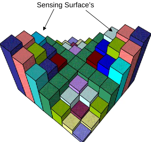
2. Design A is a 7x7 Array having 7 sensing surfaces along each x and y
axis, with 13 different elevation levels. The array side length and height is
12.04 mm and 3.18 mm respectively. The beamwidth variation is ±4° with
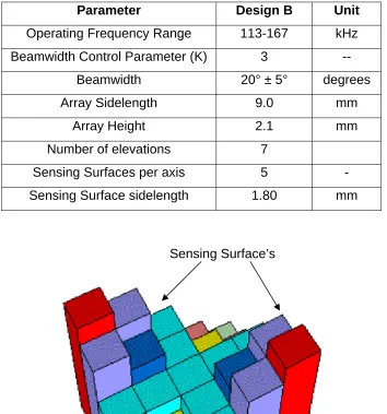
maximum sidelobe intensity of -6dB. Design B is a 5x5 Array having 5
sensing surfaces along each x and y axis, with 7 different elevation
levels. The unpackaged array sidelength and height are 9.0 mm and 2.1
mm, respectively. The beamwidth variation is ±50 with maximum sidelobe intensity of -6dB.
3. A new analytical model has been developed to accurately obtain the
capacitance change and load deflection profile of a square clamped
diaphragm. This model incorporates the effect of biasing voltage, external
pressure, fringing field and large deflections.
4. A transducer level design and performance specification for both the
designs has been obtained using lumped element model. The 3-D
Theromoelectromechanical IntelliSuite™ based FEA has been conducted
5. The fabrication process has been simulated using IntelliFab module of
IntelliSuite™. After simulation, the actual fabrication process incorporating
the fabrication constraints has been developed in conjunction with Center
of Integrated RF Engineering (CIRFE) of the University of Waterloo. The
actual SOI based fabrication of the design B was pursued at CIRFE.
Design A was not pursued for fabrication owing to its complex assembling,
packaging requirements, and cost involvement.
6. The developed assembly and packaging methodology has been
implemented at the AdvoTech Company Inc., Tempe, Arizona, USA to
realize the CMUT microarray.
1.9 Organization of Thesis
The Thesis has been organized in the following way:-
In chapter two the array theory developed earlier is used to design the
array for the target application. The basic theory behind and the mathematical
model for designing discrete hyperbolic paraboloid is presented. The physical
parameters of the array have been evaluated using the existing theory. This
mathematical model is independent of fabrication technology.
Chapter three deals with the design and simulation of the transducer used,
i.e. CMUTs. Since the CMUTs work on the basic principle of capacitance
change due to a diaphragm deflection, a novel and easy to implement
mathematical model has been developed for rapid determination of the
capacitance change and diaphragm deflection profile. This model incorporates
the effects of biasing voltage, fringing field capacitance, external pressure,
diaphragm geometry and material properties. Lumped element modeling of the
analytical modeling have been cross-verified with results from 3-D
electromechanical finite element analysis with excellent accuracy.
Chapter four deals in detail with the fabrication of the CMUTs. The
materials used, various fabrication steps and the involved recipes are provided.
The conceptual, simulation and actual photographs at various stages have also
been provided.
In chapter five assembly and packaging details of the final array has been
discussed in detail.
Chapter six makes the concluding remarks, discussions and future scope
of in this specific research area.
Chapter 2
Micro-Array Theory
In this chapter detailed design procedure to determine the array level
specifications of a discretized hyperbolic paraboloid geometry CMUT array for
the target automotive blind spot detection application has been presented. The
background of the theory used to develop the array shape and its macro model
has been reviewed in detail. Further, the design developed in [6] for MEMS
based implementation has been reviewed. Step by step details of the array level
design is presented. Once the desired operating frequency range, beamwidth
and acceptable beamwidth variation within the operating frequency range are
specified, the methodology enables to determine the geometric specification for
the array. Transducer level design has been discussed in detail in the next
chapter.
2.1 Background
Different approaches to implement constant beamwidth beamforming
sensor arrays are available in [1, 5, 8-9]. However, all of them need complex
algorithms implemented using a digital signal processing engine to realize a
beamforming and beamsteering capability. Although these beamforming
techniques produce the desired results to acceptable extent; however, they are
complex in nature and the power, cost and time delay associated with the signal
real time characteristic of the beamforming function is crucial. In [10], it has been
established that a frequency independent constant beamwidth beamforming
(FICBB) transducer array can be realized by exploiting the surface topology of
the array geometry instead of using a microelectronics based digital signal
processing beamforming engine. The basic idea behind this line of thought
comes from the Synthesis array theory [42].
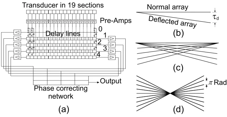
Following the Synthesis array theory, a reasonably constant beamwidth
can be achieved if several basic beam patterns from a linear array of
close proximity transducers can be superimposed in a spatially deflected
manner. A graphical representation of the synthesis method
) /( ) (x x
Sin
[10] has been shown
is fig 2.1. Following fig 2.1, several delay lines are used to deflect the basic beam
patterns in such a manner that the resulting beamwidth of the array widens at the
same rate as the angular beamwidth decreases with frequency. Finally, by using
a phase correcting network, the beampatterns are combined in such a way that
the phase at the centers of all arrays becomes identical, or in physical terms, the
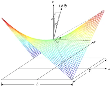
A hyperbolic paraboloid surface, as shown in fig 2.2, satisfies the
requirement of intrinsic beamforming as suggested by [4, 6, 10]. A square
footprint hyperbolic paraboloid surface can be expressed in Cartesian coordinate
as:
⎟ ⎠ ⎞ ⎜ ⎝ ⎛ =
L x y
z tan 2α
Where x, y and z are the Cartesian coordinates, L is the sidelength in terms of
wavelengths along the x and y directions, respectively and α is the amount of
out-of-plane twist in the z direction at the surface extremity measured in degrees from
the center of the surface as shown in fig 2.3.
Figure 2.2. A hyperbolic paraboloid surface.
Assuming that the out-of-plane angle α is small, the generalized array factor
) (θ,φ
f of a continuous aperture hyperbolic paraboloid geometry array in a given
direction (θ,φ)as referenced from the array normal can be expressed as [10]:
dydx e LY ) , ( f L L Y Y L xy tan y tan x t j
∫ ∫
− − ⎟ ⎠ ⎞ ⎜ ⎝ ⎛ + + = 2 2 2 2 2 21 π θ φ α
φ
θ (2.2)
where Y and L are the array sidelength along the yand x directions, respectively.
The parameter t in (2.2) is defined as:
1 1
2
2 + +
=
φ
θ tan
tan
t (2.3)
In [10] it has been shown that the array has a reasonably constant directional
response value of 1/(2αL) for large values of L with a small out-of-plane twist
angle α. However, the array response calculated following (2.2) is valid only if the out of the plane angle α is less than or equal to 10°. For larger values of α,
mathematical assumptions made during derivations in [10] lead to considerable
error. In [10], (2.2) has been experimentally verified by measuring the array
response form a large continuous aperture hyperbolic paraboloid geometry
transducer.
Since current microfabrication techniques are basically planar processes
that involve successive deposition, patterning, and etching of thin films, a
continuous aperture hyperbolic paraboloid geometry transducer array cannot be
fabricated using the capabilities of today’s microfabrication techniques. As a
solution to this problem of fabrication incompatibility, a discretized hyperbolic
paraboloid geometry transducer array has been suggested in [4, 6]. This
discretized array can provide an intrinsic constant beamwidth beamforming
capability that can match very closely with that from a continuous aperture
double integral in (2.2) has been expressed as the sum of an infinite number of
discrete points separated by infinitesimal intervals using standard spatial
sampling techniques, such as the Riemann summation [11]. After performing the
spatial sampling, the infinite summation can be reduced to a finite one of an
arbitrary number of levels. Out of the various Riemann Summation techniques
available, center based Riemann Summation was used in this case as it is good
for non-monotonic functions and its ability to calculate error bands. Following
[14], the center-based Riemann summation in one dimension can be expressed
as: n a b n a b i a f x f n i n b a − ⎟⎟ ⎠ ⎞ ⎜⎜ ⎝ ⎛ − ⎟ ⎠ ⎞ ⎜ ⎝ ⎛ + + =
∑
∫
→∞ = 1 2 1 lim )( (2.4)
where represents the number of discretization levels. The maximum error
resulting from this approximation is given as:
n
(
)
3 2 2 12 ) ( n a b M A dx x f b a mid − ≤ −∫
(2.5)where, M2 is the maximum value of | f ′′(x)| and is the value of at the
midpoint of the interval a-b.
mid
A f(x)
Applying (2.4) to (2.2) twice, first along x axis and then along y axis, the
array factor for the discretized array can be derived as [6]:
( )
∑∑
− = − = ⎟ ⎠ ⎞ ⎜ ⎝ ⎛ + +=
1 0 1 0 ' ' 2 tan ) ' ( tan ) ' ( 21
,
M m N n L y x y x t je
MN
f
α φ θ πφ
θ
(2.6)⎟⎟ ⎠ ⎞ ⎜⎜ ⎝ ⎛ ⎟ ⎠ ⎞ ⎜ ⎝ ⎛ + + − = M L m L ' x 2 1
2 , ⎟⎟⎠
⎞ ⎜⎜ ⎝ ⎛ ⎟ ⎠ ⎞ ⎜ ⎝ ⎛ + + − = N Y n Y ' y 2 1
2 (2.7)
and M and are the number of sensing surfaces in the x and y directions
respectively.
N
2.2 Array Geometrical Specification Determination
2.2.1 Array Sidelength
The minimum sidelength S of the square footprint discretized hyperbolic
paraboloid geometry sensor array can be determined from the following relation
[6]:
lower f
Kc
S = (2.8)
where is the speed of sound in media and is the lower bound frequency
in the operating range.
c flower
K is the fitting parameter based on the amount of
acceptable beam shape variation. As the beamwidth decreases with an increase
in the frequency, empirical parameter K maintains the beamwidth within a range
of 1-100 variations for all the frequencies in a frequency range of
(
fupper / flower)
≤40. Table 2.1 lists some of the values of K for different acceptable beamwidth variation [6].Table 2.1: Beamwidth Control Parameter K Value
K (Unit less) Beamwidth Variation (°)
3 7
5 5
8 2
2.1.2 Number of Sensing Surfaces
It has been observed that a linear relationship exists between the number
of sensing surfaces and the maximum operating frequency for a pre-specified
sidelobe power. Based on numerical simulation results, this relationship has
been formulated mathematically using a least-square data-fitting technique to
minimize the sidelobe power for all the frequencies in the target range below
some pre-specified level while optimizing the number of sensing surfaces M and N in each direction.
The resulting equations (2.9) and (2.10) specify the number of sensing
surfaces per axis for a square footprint array for -10dB and -6dB sidelobe
powers, respectively ⎥ ⎥ ⎦ ⎤ ⎢ ⎢ ⎣ ⎡ − ⎟ ⎟ ⎠ ⎞ ⎜ ⎜ ⎝ ⎛ ×
= 5.69 0.8637
, 5695 . 0 upper S N M λ (2.9) ⎥ ⎥ ⎦ ⎤ ⎢ ⎢ ⎣ ⎡ − ⎟ ⎟ ⎠ ⎞ ⎜ ⎜ ⎝ ⎛ ×
= 1.49 0.8484
, 9029 . 0 upper S N M
λ (2.10)
2.1.3 Array Height
The height of the array is directly related to the out of plane twist present
at the array extremities. The maximum height measured from the center of a
continuous aperture hyperbolic paraboloid geometry array can be determined
from the out of plane twist angle α as S.tanα, where S is the sidelength of the array as determined in section 2.2.1. Figure 2.4 shows the relation in a graphical
form.
A slight reduction in array height takes place due to the sampling point not
shown in fig 2.4. However this sampling error introduces an angular error of less
than 4.0% for arrays with more than 5 sensing surfaces per axis. This affects the
beamwidth by less than 1o [6].
The total height (H) for a discretized square footprint array geometry can
be determined using equation (2.11), which has been developed using a curve
fitting technique from numerical simulation results obtained using MatlabTM for an out of plane twist angle of 100 [4] .
(
)
0792 0
10 3762 0 5215
0. M . S.α
H = − × − . +
(2.11)
where M representsthe number of sensing surfaces in each x and y axis.
Figure 2.4. Array height sampling
2.3 Array Design for Blind Spot detection
The array geometric design starts with the specifications of the desired
operating parameters such as frequency range, beamwidth, and acceptable
beamwidth variation. Once the specifications for these parameters are given, the
design methodology presented above enables one to determine the necessary
For the target application of Blind spot detection in automobiles the
sensor’s operating frequency range should be 113-167 KHz and the maximum
sidelobe intensity of less than -6dB [12-13]. Based on these design requirements,
two separate designs, design A and design B have been proposed. Table 2.2
lists the determined array geometrical specifications for Design A and a
conceptual geometry of design A is shown in figure 2.5. Table 2.3 lists the
determined array geometrical specifications for Design B and a conceptual
geometry of design B is shown in figure 2.6. The fabrication and assembly
constraints have been discussed and incorporated in chapter 4.
Table 2.2. Array Geometrical Specification for Design A
Parameter Design A Unit
Operating Frequency Range 113-167 kHz
Beamwidth Control Parameter (K) 4 --
Beamwidth 20° ± 4° degrees
Array Sidelength 12.04 mm
Array Height 3.18 mm
Number of elevations 13
Sensing Surfaces per axis 7 -
Sensing Surface’s
Table 2.3. Array Geometrical Specifications for Design B
Parameter Design B Unit
Operating Frequency Range 113-167 kHz
Beamwidth Control Parameter (K) 3 --
Beamwidth 20° ± 5° degrees
Array Sidelength 9.0 mm
Array Height 2.1 mm
Number of elevations 7
Sensing Surfaces per axis 5 -
Sensing Surface sidelength 1.80 mm
Sensing Surface’s
Chapter 3
CMUT Design and Simulation
This chapter describes the detailed design methodology adopted to design the capacitive micromachined ultrasonic transducers (CMUTs). The mathematical models used to obtain the electrical design, mechanical design and performance parameters have been discussed in detail. A highly accurate analytical model has been developed to calculate capacitance change and deflection profile for MEMS-based capacitive sensors with square membranes. The device performance has been verified using IntelliSuite™.
3.1 Capacitive Micromachined Ultrasonic Transducers
(CMUTs): Operating Principle
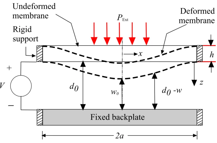
Figure 3.1. Basic Structure of a Capacitive Sensor with a Square Membrane
When exposed to an acoustical sound wave or fluid pressure , the
membrane deflects causing a decrease in the initial airgap that result in an
increase in the capacitance between the membrane and the fixed backplate. To accommodate this increase in capacitance, charges flow from the battery towards the sensor electrodes. When the pressure is withdrawn, the membrane moves back to its undeflected position, the gap increases, and the capacitance decreases. To match this capacitance change, charges flow away from the sensor electrodes towards the battery. In this way, as the membrane vibrates due to an incident acoustical wave or pressure, charges keep flowing to and away from the sensor geometry. When an AC voltage is applied between the electrodes in addition to the bias voltage, a sinusoidal vibration of the membrane is obtained, also known as Transmitting mode. Thus, the same capacitive sensor can be used both as a receiver and as a transmitter.
Ext
P
3.2 New Analytical Model for Capacitance Change
3.2.1 Capacitance Change
The capacitance between a VLSI on-chip interconnect of length , width W and thickness separated from an underneath silicon substrate by a dielectric
medium of thickness can be expressed as [35]:
L h 0 d ⎥ ⎥ ⎦ ⎤ ⎢ ⎢ ⎣ ⎡ ⎟ ⎠ ⎞ ⎜ ⎝ ⎛ + ⎟ ⎠ ⎞ ⎜ ⎝ ⎛ + + = 5 . 0 0 25 . 0 0 0 06 . 1 06 . 1 77 . 0 d h d W d W L ε
C (3.1)
where ε =ε0εr, ε0 is the permittivity of free space and εr is the relative
permittivity of the dielectric layer. The quantity ε0LW d0 in (3.1) is simply the
parallel plate capacitance. The second term within the square bracket is a length ( ) dependent adjustment parameter. The third term represents the fringing field capacitance due to the interconnect width (W) while the fourth term represents the fringing field capacitance due to the interconnect thickness ( ). Equation (3.1) can be rewritten to express the fringing field capacitances as a function of the parallel plate capacitance in the form:
L h ) 1 ( ff 0 C C
C= + (3.2)
where C0 is the parallel plate capacitance (ε0LW/d0) and is the fringing field factor expressed as:
ff C W hd W d W d
C o o
5 . 0 0 75 . 0 ff ) ( 06 . 1 06 . 1 77 .
0 ⎟ +
⎠ ⎞ ⎜ ⎝ ⎛ +
Equations (3.1)-(3.3) can be used to calculate the capacitance between the thin square membrane and the fixed backplate of a CMUT as shown in fig. 1.1. As the membrane is rigidly clamped at the edges and is supported by a dielectric spacer, third term in (3.3) representing the fringing field factor due to the membrane thickness can be neglected as the flux lines originating from the membrane sides don’t have any path to terminate on the backplate. Thus, for a square membrane with sidelength W=L=2a, the capacitance between the
undeflected membrane and the backplate can be expressed as:
⎥ ⎥ ⎦ ⎤ ⎢ ⎢ ⎣ ⎡ ⎟ ⎠ ⎞ ⎜ ⎝ ⎛ + ⎟ ⎠ ⎞ ⎜ ⎝ ⎛ + = + = 75 . 0 0 0 0 2 0 ff 0 2 06 . 1 2 77 . 0 1 4 ) 1 ( a d a d d a C C
C ε (3.4)
As in the undeformed case, the total capacitance of a deformed membrane under external pressure is also contributed by two factors: the parallel plate capacitance between the deformed diaphragm and the backplate,
and the fringing field capacitance which can be expressed as:
Deform C ff DeformC C ) 1 ( ff Deform C C
C= + (3.5)
Since the edges of the membrane are rigidly fixed and don’t undergo any deformation, and as the fringing field is contributed mainly by the charges
concentrated at the edges, the fringing field factor can be assumed to remain
unchanged due to the deformation of the membrane and can be calculated
using (3.3) as before.
ff
C
ff
Assuming that the diaphragms lies in the x– y plane, the parallel plate capacitance between the deformed membrane and the backplate can be calculated following [36] as:
( )
∫∫
−=
A o
o d w x y
dxdy
ε
C
,
Deform (3.6)
where is vertical displacement of any point on the membrane located at
and can be determined from the center deflection using the following relation originally proposed in [37]:
(
x y w ,)
)
(
x,y w0( )
⎟
⎠
⎞
⎜
⎝
⎛
⎟
⎠
⎞
⎜
⎝
⎛
=
a
y
cos
a
x
cos
w
y
,
x
w
2
2
0π
π
(3.7)The above deflection shape function satisfies the boundary condition of zero
bending at the edges. It was observed in [38] that the cosine-like bending shape
as expressed in (3.7) does not describe the membrane’s actual bending shape
accurately. In order to better describe the bending shape of a thin membrane,
(3.7) was modified in [38] by adding two more terms as:
( )
⎟ ⎠ ⎞ ⎜ ⎝ ⎛ ⎟ ⎠ ⎞ ⎜ ⎝ ⎛ ⎥ ⎦ ⎤ ⎢ ⎣ ⎡ ⎟⎟ ⎠ ⎞ ⎜⎜ ⎝ ⎛ + ⎟⎟ ⎠ ⎞ ⎜⎜ ⎝ ⎛ + + = a y π a x π a y x w a y x w w y x w o 2 cos 2 cos , 4 2 2 2 2 2 2where and are two arbitrary parameters expressed as multiples of .
Using the energy minimization method, authors in [38] numerically determined parameters and as:
1
w w2 w0
1
w w2
⎭ ⎬ ⎫ = = 0 2 0 1 16 . 1 4 . 0 w w w w (3.9)
Though the deflection shape function (3.8) shows excellent agreement with experimental results for deflection profiles of thin diaphragms, investigation shows it does not agree well with the deflection shapes of thick diaphragms that behave more like plates. Further, (3.8) starts deviating for thinner diaphragms with side length less than 1 mm. Authors in [36, 39] used the following deflection shape function for clamped square diaphragm:
( )
⎟ ⎠ ⎞ ⎜ ⎝ ⎛ ⎟ ⎠ ⎞ ⎜ ⎝ ⎛ = a y a x w y x w 2 cos 2 cos, 0 2 π 2 π (3.10)
This shape function also satisfies the two necessary boundary conditions for a clamped square diaphragm, namely the zero deflection and zero gradients in the deflection profile at diaphragm edge, expressed as [39]:
⎪
⎪
⎭
⎪⎪
⎬
⎫
±
=
=
=
±
=
=
=
a
y
dy
dw
w
a
x
dx
dw
w
at
0
and
0
at
0
and
0
(3.11)deflection shape function presented in [39] when compared to FEA results. However, though (3.10) is a poor match for thin membrane deflection profiles, it satisfies the necessary boundary conditions for a clamped square membrane [36, 39]. Therefore, following the approach adopted by the authors in [38], we attempt to extend the deflection shape function in [39] with three more terms with coefficients w1, w2 and w3. The resulting deflection shape function is as follows:
( )
⎟ ⎠ ⎞ ⎜ ⎝ ⎛ ⎟ ⎠ ⎞ ⎜ ⎝ ⎛ ⎥ ⎦ ⎤ ⎢ ⎣ ⎡ ⎟⎟ ⎠ ⎞ ⎜⎜ ⎝ ⎛ + + ⎟⎟ ⎠ ⎞ ⎜⎜ ⎝ ⎛ + ⎟⎟ ⎠ ⎞ ⎜⎜ ⎝ ⎛ + + = a y π a x π a y x w a y x w a y x w w y x w 2 cos 2 cos, 4 2 2
4 4 3 4 2 2 2 2 2 2 1
0 (3.12)
where the coefficients , , and can be determined for any specific design
space by comparing with the deflection profiles obtained experimentally or from FEA analysis. For the typical design space for MEMS based capacitive type sensors characterized by a square membrane thickness range of 1-3 μm and a
membrane sidelength range of 200-1000 μm, the parameters , , and
have been determined by comparing the results from (3.12) with 3-D FEA using
IntelliSuite™ for a wide range of device specifications and loading conditions as:
1
w w2 w3
1
w w2 w3
where represents the membrane thickness. h
The adjustable empirical parameters , , and in (3.12) will
contribute to achieve higher accuracy and make it more suitable to fit deflection profiles for any specific design space.
1
w w2 w3
3.2.2 Electrostatic Pressure
As the DC bias voltage provides a means to realize a voltage signal having the same dynamic characteristics as the incident acoustical or mechanical pressure, the electrostatic attraction force associated with this bias voltage also causes a deflection of the diaphragm. Thus at any time, the total deflection of the diaphragm is the summation of the diaphragm deflection due to external pressure and the diaphragm deflection due to the electrostatic pressure. Thus, the change in capacitance is also a function of diaphragm deflection due to the electrostatic pressure.
Further, this electrostatic attraction force is nonlinear and increases with the decreasing gap between the electrodes for a fixed voltage. When in equilibrium, the total force acting on the diaphragm which is the sum of the electrostatic and the external mechanical pressure will be equal to the elastic restoring force developed in the diaphragm due to its deformation. Hence the effect of Electrostatic force can’t be neglected while calculating the center deflection and hence the capacitance change.
associated change in capacitance has not been considered in the previous works. Moreover, in the previous works, a parallel plate approximation has been used to calculate the capacitance before and after deformation. However, investigation shows that fringing field capacitance associated with the diaphragm edges also contribute to the total capacitance change during the deformation.
The developed electrostatic force after applying a bias voltage V can be derived from the relation:
⎟ ⎠ ⎞ ⎜ ⎝ ⎛ − = 2 2 1 CV dx d F
(
)
(
( )
)
⎥⎥⎦ ⎤ ⎢ ⎢ ⎣ ⎡ − + −= 1.25
25 . 0 2 2 0 2 265 . 0 2 w d a w d a aV ε o o (3.14)
Expanding the terms in the bracket in (3.14) using the Taylor series expansion method about the zero deflection point of the diaphragm center (w=0), neglecting the higher order terms, and after rearrangement one obtains:
( )
( )
wd a d a V ε d a d a V ε F o o o
o ⎟⎟⎠
⎞ ⎜⎜ ⎝ ⎛ + + ⎟⎟ ⎠ ⎞ ⎜⎜ ⎝ ⎛ +
= 2.25
25 . 0 3 2 2 0 25 . 1 25 . 0 2 2 2 0 2 33125 . 0 8 2 265 . 0
4 (3.15)
Thus the associated electrostatic pressure PE can be calculated from (3.15) as:
( )
( )
wd a d a a V ε d a d a a V ε A F P o o o o E ⎟⎟ ⎠ ⎞ ⎜⎜ ⎝ ⎛ + + ⎟⎟ ⎠ ⎞ ⎜⎜ ⎝ ⎛ + =
= 0 2 3 2.250.25
25 . 1 25 . 0 2 2 0 2 33125 . 0 4 2 2 265 . 0 2
2 (3.16)
where A is the area of the diaphragm. However, as the actual diaphragm motion
isn’t piston like and the deformation profile of the diaphragm takes a cosine
shape, maximum deflection occurs at the center of the diaphragm. Thus,
replacing by in (3.16) one obtains the load deflection model of a square
0 w
diaphragm subject to a linearized electrostatic pressure due to an applied bias voltage V .
3.2.3 Center Deflection
The load-deflection model of a rigidly clamped square diaphragm under large deflection due to an applied uniform pressure PExt can be expressed as [19]:
( )
34 4 2 ~ 12 o s s o b o r a σ ext w a h E ν f C w a D C w h C
P = + + (3.17)
where is the center deflection, is the diaphragm sidelength and h
represents the thickness of the diaphragm. In (3.17)
0
w 2a
E~ and represent the effective Young’s modulus and the Poisson ratio of the diaphragm material, respectively. C
v
r, Cb and Cs are constants and are equal to 3.45, 4.06 and 1.994,
respectively and fs
( )
ν , a function of ν , is given by [38]:( )
ν ν ν fs − − = 1 271 . 0 1 (3.18)In (3.17) D represents the flexural rigidity of the diaphragm and is expressed as:
) ( h E~ D 2 3 1 12 −ν
= (3.19)
2
1
~
ν
−
=
E
E
(3.20)where E represents the original Young’s modulus of the diaphragm material. In equation (3.17), the first term on the right-hand side represents the deflection of the diaphragm due to the residual stress; second term is the deflection due to bending and the third term represent the deflection due to nonlinear spring hardening.
3.2.4 Combined Load Deflection Model
A combined load deflection model of the square diaphragm under electrostatic and external mechanical pressure thus can be obtained by combining (3.16) and (3.17). After combination and rearrangement, one obtains :
( )
oo o b r o s s w d a d a V ε a a D C a h σ C w a h E ν f C ⎥ ⎥ ⎥ ⎥ ⎦ ⎤ ⎢ ⎢ ⎢ ⎢ ⎣ ⎡ ⎟⎟ ⎠ ⎞ ⎜⎜ ⎝ ⎛ + − + + 25 . 2 25 . 0 3 2 0 4 2 3 4 33125 . 0 2 2 1 12 0 265 . 0 2 1 25 . 1 25 . 0 2 2
0 ⎥ =
⎦ ⎤ ⎢ ⎣ ⎡ ⎟⎟ ⎠ ⎞ ⎜⎜ ⎝ ⎛ + + − o o M d a d a V ε a
P . (3.21)
Real root of the above third-order polynomial represents the center deflection of the diaphragm subject to both electrostatic and external
pressure. Two other roots are imaginary and have no practical significance. Once the center deflection is known, over-all deflection profile of the diaphragm can be obtained using (3.12) and also the capacitance change using (3.6). This
o
methodology has also been used to obtain the pull-in voltage and the results have been verified by FEA simulations.
3.3 CMUT Lumped Element Model
After determination of the array geometric specifications (Chapter two), transducer level modeling is done to obtain the geometry of individual capacitive sensors and optimize the performance of the sensor. Lumped element modeling is used to reduce the geometric complexity to a manageable level for rapid simulation and specification determination. The lumped element modelling is able to optimize the performance of the individual transducers. This includes modeling of all major sensor performance criteria such as, pull-in voltage, resonant frequency, damping effects and load deflection characteristics [21, 23, 24].
The sensitivity of the CMUT depends mainly on the size and stress of the diaphragm, thickness of the airgap, and the bias voltage.
The sensitivity and the frequency response of the CMUT can be calculated using an equivalent analog electrical network model of the CMUT [21] as shown in figure 3.2.
In Fig. 3.2, the acoustical force is modeled as an equivalent voltage
source and the radiative resistance is . The air mass in contact with the
diaphragm subject to displacement is represented by . Theses parameters
are defined as [21]:
sound F r R r M c π ω a ρ Rr 2 4 4 0
= (3.22)
π π a ρ Mr 3 8 0 3
= (3.23)
Where is the air density, a is the diaphragm sidelength, is the angular
vibration frequency and c is the velocity of sound in the media at frequency
. The mechanical mass of the diaphragm and the diaphragm compliance
which is the inverse of the diaphragm stiffness (spring constant) are
expressed as. 0 ρ ω fc π 2
ω Mm
m
C
(
π D a T)
π
a Cm 6 2 2
2
2 32
+
= (3.24)
(
)
T T a D π ρ π Mm 64 2 2 24 +
= (3.25)
Viscous losses in the air gap and in the vent hole , and the gap
compliance , are given as:
g
R Rh
a C
( )
⎟⎟ ⎠ ⎞ ⎜⎜ ⎝ ⎛ − − − = 8 3 4 ln 8 2 12 2 32 α α α
π
nd a
η
Rg (3.26)
4 2 8 nr π ha η
Rh ≈ (3.27)
2 2 2 0c α a
ρ
d
Ca = (3.28)
Where is the hole density in the backplate, α is the surface fraction occupied by holes, is the air viscosity coefficient, is the average thickness of the
airgap, is the vent height and
n
η d
h r is the effective radius of the vent holes. From
these definitions we can express the equivalent impedance Zt of the CMUT as:
(
)
a h g h g m r rt jω R R C
R R C ω j M M ω j R Z ) ( 1 1 + + + + + + + = (3.29)
The total sensitivity of the CMUT is defined as the output voltage per unit
of incident acoustical pressure
t
S Vo
P and can be expressed as [21]:
t b
t jωdZ
a V P V S 2 0 =
= (3.30)
The sensitivity presented above lumps the electrical and mechanical components of the system together. This illustrates how the sensitivity scales linearly with bias voltage, but doesn’t clearly show the mechanical sensitivity. By separating the sensitivity model between the mechanical and electrical components of the transducer, each component can be evaluated and optimized independently [23]. The mechanical sensitivity can be given in μm/μN as:
m a z
C C S
1 1
1
+
= (3.31)
3.4 Design Performance and Verification
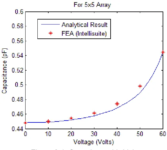
The theory discussed in the previous sections has been implemented using Matlab™. The result for both the designs A and B have been presented in this section. The IntelliSuite™ 3D electromechanical Analysis has been carried out wherever appropriate. All the Matlab™ codes have been provided in Appendix A. However it has to be noted that only design B (5x5 Array) has been persuaded for fabrication owing to its less complex alignment and packaging requirements. Table 3.1 and 3.2 provides the transducer design specifications and performance specifications for design A (7x7 Array), respectively. Table 3.3 and 3.4 provides the transducer design specifications and performance specifications for design B (5x5 Array), respectively.
shows the relation between capacitance and applied voltage. Both the results have been verified by FEA simulation and are in excellent agreement with the model developed. Figure 3.5 shows the relation between center deflection and pressure at 18 volts biasing voltage. These results show that the effect of applied voltage can’t be neglected while calculating either capacitance change or deflection profile.
Table 3.1. Transducer Design Specifications (7x7Array)
Specifications Value Unit
Diaphragm per Tier 64 -
Diaphragm Thickness 2.0 μm
Diaphragm Air Gap 1.0 μm
Diaphragm Side length 215 μm
Number of vent holes 4x4 -
Vent Hole dimension 15x15 μm
Table 3.2. Transducer Performance Specifications (7x7Array)
Parameter Value Unit
Pull in Voltage 63.53 Volts
Unbiased Tier Capacitance 26.2 pF
Resonant Frequency 512.9 kHz
Table 3.3. Transducer Design Specifications (5x5Array)
Specifications Value Unit
Diaphragm per Tier 6x6 -
Diaphragm Thickness 2.0 μm
Diaphragm Air Gap 1.0 μm
Diaphragm Side length 225 μm
Number of vent holes 5x5 -
Vent Hole dimension 15x15 μm
Inter Dia. Spacing 20 μm
Bonding Space (edges) 175 μm
Table 3.4. Transducer Performance Specifications (5x5Array)
Parameter Value Unit
Pull in Voltage 51.72 Volts
Unbiased Tier Capacitance 16.12 pF
Resonant Frequency 480.19 kHz
Figure 3.3. Center Deflection Vs Voltage
Figure 3.5. Center Deflection Vs Pressure
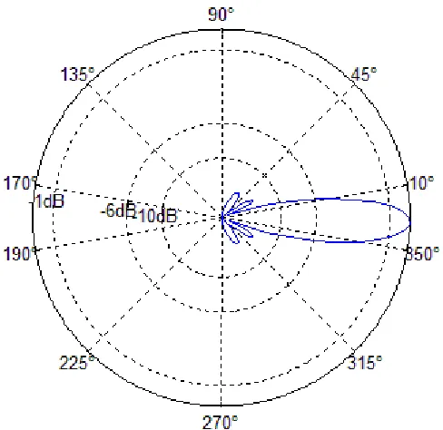
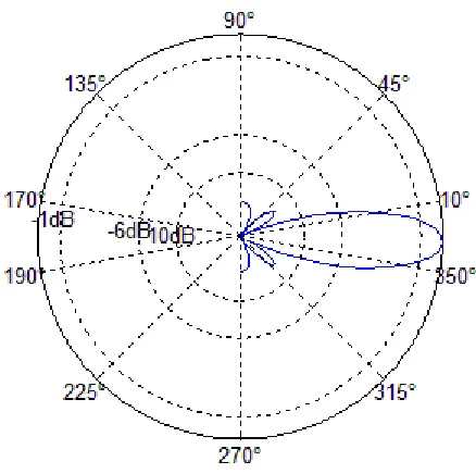
3.5 Beam Shapes
In order to simulate the beamforming capability of the designs, there array factors (as given in chapter two) have been plotted using polar plots. Also to verify the broadband beamforming claim, the beam shapes at various frequencies in the desired range have been obtained. Figure 3.8-3.10 and figure 3.11-3.13 show the beam shapes for design A (7x7 Array) and design B (5x5 Array) respectively. The Matlab code for the same has been provided in Appendix A.
Figure 3.9. 7x7 Array Beam Shape at 140 kHz
Figure 3.11. 5x5 Array Beam Shape at 113 kHz
Chapter 4
Fabrication
This chapter deals in detail with the fabrication methodology used to fabricate the Capacitive Micromachined Ultrasonic Transducers (CMUT). Each fabrication step description has been provided with the operating conditions, used materials, process type, conceptual cross sectional view and fabrication simulation result from IntellisuiteTM. For proof of concept, the fabrication of 5x5 Array was carried out due to its less complex alignment and packaging process. The whole fabrication process was carried out at the Center of Integrated Radio Frequency Engineering (CIRFE), University of Waterloo.
4.1 Array Fabrication Details
An SOI (Silicon-On-Insulator) based fabrication process has been adopted. As compared to other diaphragm material like Si3N4 and Polysilicon, the latest SOI based technology has been preferred for the following advantages:
1. Higher switching speeds [25] 2. Higher quality factor
3. Lower value of residual stress 4. Thickness uniformity
6. Reduction in fabrication steps 7. Lower number of masks 8. Reduction of cost [26]
The microarray has 5 sensing surfaces along each x and y axis. The detailed
specification of the SOI wafers used is provided in Table 4.1. The complete fabrication process consists of 8 major steps including dicing. The colors associated with the materials used are shown in fig 4.1.
Table 4.1. SOI Wafer Specifications
Parameter Specification(s)
Diameter 150±0.2 mm
Crystal Orientation <100> Overall Thickness 352±5 µm Front side finished Polished
Back Side Finished Nanogrind @2000 mesh
Device Layer
Thickness 2±0.5 µm
Type/Dopant n/Sb
Resistivity <0.2 Ohmcm
Handle wafer
Thickness 350±5 µm
Type/Dopant n/Phos
Resistivity <5 Ohmcm
Buried Oxide
Thermal Oxide 1±5% µm
4.2 Fabrication Process
Step 1: RCA Clean
The wafers are subject to a RCA cleaning before any of the fabrication process can be carried out. The purpose of the cleaning is to remove all organic contamination, oxide film or heavy metal contamination from the wafer. The RCA solution is prepared by adding 130 ml of Hydrogen Peroxide into 600 ml of DI water. Then 130 ml of Ammonium Hydroxide is added to the same sample. The sample is then heated to 70±50C using a hot plate. A Teflon holder is used to put the wafer into the solution for 15 minutes. The wafers are then carefully placed under de-Ionized (DI) water tap for approx. 5 minutes so that the RCA solution is flushed out and then dried using a Nitrogen gun [27]. The conceptual, IntelliSuite™ generated and actual photograph has been shown in figure 4.2.
(a)
Figure 4.2. Fabrication step 1 details IntelliSuiteTM
(b)
Step 2: Metal Deposition (Gold and Chromium)
eaning is to deposit the conducti Si device
ion layer. A 25 nm layer of Chromium
ited using electron-beam evaporation method. Nanochrome deposition system available at the CIR
ition of both chromium and gold. Chromium seed lay of 3.0 Å/sec and Gold conduc power which gives a rate
to avoi
and actual fabrication image are shown
The next step after cl ve Gold (Au) layer.
Since gold can’t be directly deposited on layer, chromium is first
deposited to act as an adhes and then 200
nm of gold layer is depos
IntelvacTM FE clean room is
used for the depos er was
deposited at 20% power which gives a rate tive
layer was deposited at 30% of 9.2 Å /sec. The two processes are done in one duty cycle in order d oxidation of chromium. The conceptual figure, simulation result
in figure 4.3 (a)-(c).
(a) (b)
Figure 4.3. Fabrication step 2 details. (a) Conceptual cross-section, (b) IntelliSuiteTM generated 3-D model.
Before