University of Windsor University of Windsor
Scholarship at UWindsor
Scholarship at UWindsor
Electronic Theses and Dissertations Theses, Dissertations, and Major Papers
2013
A 5 meter range non-planar CMUT array for Automotive Collision
A 5 meter range non-planar CMUT array for Automotive Collision
Avoidance
Avoidance
Jonathan Hernandez Aguirre University of Windsor
Follow this and additional works at: https://scholar.uwindsor.ca/etd
Recommended Citation Recommended Citation
Hernandez Aguirre, Jonathan, "A 5 meter range non-planar CMUT array for Automotive Collision Avoidance" (2013). Electronic Theses and Dissertations. 4875.
https://scholar.uwindsor.ca/etd/4875
This online database contains the full-text of PhD dissertations and Masters’ theses of University of Windsor students from 1954 forward. These documents are made available for personal study and research purposes only, in accordance with the Canadian Copyright Act and the Creative Commons license—CC BY-NC-ND (Attribution, Non-Commercial, No Derivative Works). Under this license, works must always be attributed to the copyright holder (original author), cannot be used for any commercial purposes, and may not be altered. Any other use would require the permission of the copyright holder. Students may inquire about withdrawing their dissertation and/or thesis from this database. For additional inquiries, please contact the repository administrator via email
A 5 meter range non-planar CMUT array for Automotive Collision
Avoidance
By
Jonathan Hernandez Aguirre
A Thesis
Submitted to the Faculty of Graduate Studies
through Electrical and Computer Engineering
in Partial Fulfillment of the Requirements for
the Degree of Master of Science at the University of Windsor
Windsor, Ontario, Canada
2013
A 5 Meter Range Non-Planar CMUT Array for Automotive
Collision Avoidance
by
Jonathan Hernandez Aguirre
APPROVED BY:
______________________________________________
. R. Rashidzadeh, Department of Electrical and Computer Engineering
______________________________________________
A. Riahi, Department of Mechanical, Automotive and Materials Engineering
______________________________________________
. S. Chowdhury, Advisor, Department of Electrical and Computer Engineering
iii
DECLARATION OF ORIGINALITY
I hereby certify that I am the sole author of this thesis and that no part of this thesis has been
published or submitted for publication.
I certify that, to the best of my knowledge, my thesis does not infringe upon anyone’s copyright
nor violate any proprietary rights and that any ideas, techniques, quotations, or any other
material from the work of other people included in my thesis, published or otherwise, are fully
acknowledged in accordance with the standard referencing practices. Furthermore, to the
extent that I have included copyrighted material that surpasses the bounds of fair dealing within
the meaning of the Canada Copyright Act, I certify that I have obtained a written permission
from the copyright owner(s) to include such material(s) in my thesis and have included copies of
such copyright clearances to my appendix.
I declare that this is a true copy of my thesis, including any final revisions, as approved by my
thesis committee and the Graduate Studies office, and that this thesis has not been submitted
iv
ABSTRACT
A discretized hyperbolic paraboloid geometry capacitive micromachined ultrasonic transducer
(CMUT) array has been designed and fabricated for automotive collision avoidance. The array is
designed to operate at 40 kHz, beamwidth of 40˚ with a maximum sidelobe intensity of -10dB.
An SOI based fabrication technology has been used for the 5x5 array with 5 sensing surfaces
along each x and y axis and 7 elevation levels. An assembly and packaging technique has been
developed to realize the non-planar geometry in a PGA-68 package.
A highly accurate mathematical method has been presented for analytical characterization of
capacitive micromachined ultrasonic transducers (CMUTs) built with square diaphragms. The
method uses a new two-dimensional polynomial function to more accurately predict the
deflection curve of a multilayer square diaphragm subject to both mechanical and electrostatic
pressure and a new capacitance model that takes into account the contribution of the fringing
v
DEDICATION
To my father Rogelio Hernandez Dominguez that with the work of their hands and the sweat of
his brow showed me the right path to follow in life and made me the man I’m.
To my mother Maria de la Luz Aguirre Castaneda whose infinite love and understanding taught
me to never stop enjoying the small things of the life.
vi
ACKNOWLEDGEMENTS
First, a large thank-you to my advisor Dr. Sazzadur Chowdhury, without his help this project
would not have come to completion.
I would like to thank CONACYT (National Council of Science and Technology of Mexico) for their
financial support and also Canadian Microelectronic Corporation (CMC) and IntelliSuite™ for
vii
TABLE OF CONTENTS
DECLARATION OF ORIGINALITY ... iii
ABSTRACT ... iv
DEDICATION ...v
ACKNOWLEDGEMENTS ... vi
LIST OF TABLES ... ix
LIST OF FIGURES ...x
1
CHAPTER 1 INTRODUCTION ...1
1.1 Goals ... 1
1.1.1 Research Objective ... 1
1.1.2 Background ... 1
1.2 Capacitive Micromachined Ultrasonic Transducers ... 9
1.2.1 Description ... 9
1.2.2 Benefits of CMUTs ... 12
1.3 Overview of MEMS fabrication technology. ... 14
1.3.1 Bulk micromachining ... 15
1.3.2 Sputtering ... 16
1.3.3 Spin coating ... 17
1.3.4 Wafer Bonding ... 18
1.4 Packaging Techniques ... 21
1.4.1 Adhesive Bonding ... 21
1.4.2 Wirebonding ... 22
1.5 Specific Research Objectives ... 22
1.6 Principle Results ... 23
1.7 Thesis Organization ... 24
viii
2.1 Non – Planar Array Theory ... 26
2.1.1 Beamforming ... 27
2.1.2 Array Sidelength Determination ... 31
2.1.3 Number of Sensing Surfaces Determination ... 32
2.1.4 Array Height ... 32
2.2 Model Validation ... 34
2.3 Design Methodology Non-Planar Array ... 37
2.3.1 Non-Planar Array Design ... 38
3
CHAPTER 3 CMUT DESIGN ...41
3.1 CMUT Mathematical Model ... 41
3.1.1 Center Defection of a CMUT Diaphragm ... 42
3.1.2 Deflection Shape Function ... 47
3.1.3 Capacitance ... 51
3.2 Design Methodology Sensing Surface... 54
3.2.1 Parallel-plate Capacitor Model for CMUT ... 55
3.2.2 Output Pressure Transmitted ... 57
3.2.3 Resonant Frequency ... 59
3.2.4 Pull-in and Working Voltage ... 60
3.2.5 Receive Sensitivity ... 61
3.3 Final Design Specifications ... 62
4
CHAPTER 4 DESIGN VERIFICATION ...69
4.1 Simulink Model ... 74
5
CHAPTER 5 FABRICATION ...79
5.1 Array Fabrication Details ... 79
5.2 Fabrication Process Steps ... 83
5.3 Packaging Process ... 94
6
CHAPTER 6 CONCLUSIONS AND FUTURE DIRECTIONS ...103
6.1 Future directions ... 105
REFERENCES ...106
ix
LIST OF TABLES
Table 1-1 Comparison of transducers technologies ... 14
Table 2-1 Beamwidth Control Parameter K Values ... 32
Table 2-2 Non-planar array dimensions for different working parameters ... 37
Table 2-3 Array Geometrical Specification ... 39
Table 3-1 Final CMUT Design Specification... 63
Table 3-2 Final Sensor Design Specifications ... 67
Table 4-1 Pull-in Voltage Comparison Table ... 71
Table 4-2 Resonant Frequency Comparison Table ... 71
x
LIST OF FIGURES
Figure 1-1 Ultrasonic sensors and radar for range detection and blindspot warning ... 7
Figure 1-2 CMUT Cross Section ... 10
Figure 1-3 CMUT Modes of Operation ... 11
Figure 1-4 Isotropic etch process ... 16
Figure 1-5 Ion Beam Sputtering ... 17
Figure 1-6 Spin Process ... 18
Figure 2-1. A hyperbolic paraboloid surface ... 27
Figure 2-2 Out of plane twist angle α in a Hyperbolic Paraboloid ... 28
Figure 2-3 Array Height ... 33
Figure 2-4 Discrete Array Height Sampling ... 33
Figure 2-5 A graphical representation of the discretization process of a hyperbolic paraboloid geometry ... 34
Figure 2-6 Beam shape, array length 1.6 lambda ... 35
Figure 2-7 Beam shape, array length 1.8 lambda ... 35
Figure 2-8 Beam shape, array length 2 lambda ... 36
Figure 2-9 Beam shape, array length 2.5 lambda ... 36
Figure 2-10 Conceptual Geometry of Non-Planar Array. Sensors having same elevation have same color ... 40
Figure 3-1 A section of a multilayered laminated plate ... 46
xi
Figure 3-3 Parallel-plate capacitor model for CMUTs ... 55
Figure 3-4 Single Tier Layout ... 65
Figure 3-5 Non-Planar Array Beam Shape ... 68
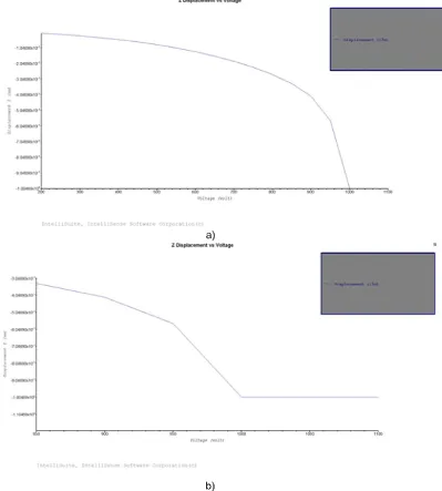
Figure 4-1 FEA displacement vs voltage graph. ... 70
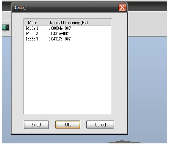
Figure 4-2 Resonant Frequency from FEA ... 71
Figure 4-3 Capacitance vs voltage (with fringing fields) ... 73
Figure 4-4 Capacitance vs voltage (without fringing fields) ... 73
Figure 4-5 Center Deflection vs voltage ... 74
Figure 4-6 Simulink model of a CMUT ... 75
Figure 4-7 Simulink model of a CMUT (subsystem) ... 75
Figure 4-8 Simulink diagram of an electrostatic force subsystem in Fig 3-10 ... 76
Figure 4-9 Simulink diagram of a CMUT membrane in Fig 3-10 ... 76
Figure 4-10 Output pressure from CMUT (Simulink model) ... 77
Figure 4-11 Membrane displacement from CMUT (Simulink model)... 77
Figure 5-1 Final dimensions for the non-planar array ... 80
Figure 5-2 Conceptual Image of non-planar array ... 81
Figure 5-3 Comparison between analytical and experimental values [23] ... 82
Figure 5-4 Step 1: Thinning SOI Wafer ... 85
Figure 5-5 BCB Coating (900 nm) ... 85
Figure 5-6 SEM Image showing BCB layer thickness ... 86
Figure 5-7 Close-up of the mask used to create the cavity ... 87
Figure 5-8 Making cavity in BCB layer ... 87
Figure 5-9 Resulting pattern ... 88
xii
Figure 5-11 SEM image BCB bonding (first iteration) ... 90
Figure 5-12 SEM image BCB bonding (second iteration) ... 91
Figure 5-13 SEM image BCB bonding (third iteration) ... 92
Figure 5-14 BCB Bonding... 92
Figure 5-15 CMUT after removal of silicon and BOX layers ... 93
Figure 5-16 SEM image of the CMUTs after silicon removal ... 93
Figure 5-17 CMUT Metallization ... 94
Figure 5-18 Generated CAD model for the non-planar array ... 95
Figure 5-19 Verowhite plus Fullcure835 3D printed non-planar array ... 95
Figure 5-20 Bonding pad ... 97
Figure 5-21 68 Ceramic package connections ... 98
Figure 5-22 Non-planar CMUT array ... 99
Figure 5-23 Set up to test the sensor ... 100
Figure 5-24 Receiver output 30 cm away from sensor ... 101
Figure 5-25 Receiver output 15 cm away from sensor ... 102
1
1
CHAPTER 1
INTRODUCTION
The research objective is presented in this chapter, the background of similar projects
developed in the industry are presented to realize the need of a novel, cheap and reliable
system that can meet the requirements of the industry. The basic working principle is presented
to then justify the use of the CMUT in the development of the system. A brief explanation of
some fabrication techniques used in the fabrication techniques is presented. The thesis
organization is then covered.
1.1
Goals
1.1.1
Research Objective
The objective of this project is to develop, design and fabricate a CMUT (Capacitive
Micromachined Ultrasound Transducer) array that will be used for collision avoidance and park
assistant, being those air-coupled applications a mathematical model is needed to accurate
calculate the necessary parameters that will dictate the behaviour of the array. Since is going to
be used in the automobile the array needs to be designed considering the restrictions that this
implied. A reliable and easy to implement fabrication and packaging process needs to be pursuit
in order to facilitate the manufacturability of the array and reduce the cost involved.
1.1.2
Background
A collision avoidance system is an automobile safety system designed to reduce the severity of
an accident. Also known as precrash system, forward collision warning system or collision
mitigating system, use radar and sometimes laser and camera sensors to detect an imminent
2
for extra support, move the passenger seat, position head rests to avoid whip lash, tension seat
belts and automatically apply partial or full braking to minimize impact.
In 2009 the U.S. National Highway Traffic Safety Administration (NHTSA) began studying
whether to make frontal collision warning systems and lane departure warning
systems mandatory. Several studies have been performed to introduce this technology in the
market [1].
In 2011 a question has been submitted to the European Commission regarding stimulation of
these "collision mitigation by braking" systems. The mandatory fitting of Advanced Emergency
Braking Systems in commercial vehicles will be implemented on 1 November 2013 for new
vehicle types and on 1 November 2015 for all new vehicles in the European Union [2]. This
could, according to the impact assessment [3], ultimately save around 5 000 fatalities and 50
000 serious injuries per year across the EU.
In an important 2012 study [4] by the non-profit research organization, Highway Loss Data
Institute, researchers examined how particular features of crash-avoidance systems affected the
number of claims under various forms of insurance coverage. They found two crash-avoidance
features provide the biggest benefits: (a) autonomous braking that would brake on its own, if
the driver does not, to avoid a forward collision and (b) adaptive headlights that would shift the
headlights in the direction the driver steers. Unexpectedly, they found lane departure systems
to be not helpful, and perhaps harmful, at the first 2012 stage of development.
A collision avoidance system works basically as follows:
Different sensors installed in the vehicle constantly monitor their environment, so that can
3
When an object (vehicle, pedestrian, obstacle, etc.) is detected, the system determines
whether the vehicle is in a situation that may occur imminent collision and, if so, is sent a
first warning to the driver to perform a braking maneuver to avoid the impact.
If the driver doesn’t react to the notice signals given, and the system detects that a collision is
imminent if nothing is done, automatically slows the vehicle, so the impact can be avoided or at
least reduce its severity.
Collision avoidance features are rapidly making their way into the new vehicle fleet. The most
common new technologies include forward collision warning, autonomous braking, lane
departure warning, lane departure prevention, adaptive headlights, blind spot detection, and
back-up cameras.
Several companies have included those kinds of systems in their cars; different approaches to
the problem have been taken:
Audi
The full version of the system (Pre-Sense Plus) works in four phases. In the first phase, the
system provides warning of impending accident, while the hazard warning lights are activated,
the side windows and sunroof are closed and the front seat belts are tensioned. In the second
phase, the warning is followed by light braking, strong enough to win the driver's attention. The
third phase initiates autonomous partial braking at a rate of 3 m/s². The fourth phase
decelerates the car at 5 m/s² followed by automatic deceleration at full braking power, roughly
4
A second system called (Pre-Sense Rear) is designed to reduce consequences of rear end
collisions. Sunroof and windows are closed, seat belts prepared for impact. The optional
memory seats are moved forward to protect the car occupants.
The system uses radar and video sensors and was introduced in 2010 on the 2011 Audi A8 [5].
Ford
Ford's Collision Warning with Brake Support was introduced in 2009 on the Lincoln MKS and
MKT and the Ford Taurus [6]. This system provides a warning through a Head Up Display that
visually resembles brake lamps. If the driver does not react, the system pre-charges the brakes
and increases the brake assist sensitivity to maximize driver braking performance.
Honda
Honda's Collision Mitigation Brake System (CMBS, although originally introduced with the initials
CMS) introduced in 2003 on the Inspire [7] (and later in Acura, Honda's luxury brand in Canada
and the United States) uses a radar-based system to monitor the situation ahead and provide
automatic braking if the driver does not react to a warning in the instrument cluster and a
tightening of the seat belts. The Honda system was the world's first production system to
provide automatic braking. The 2003 Honda system also incorporated an "E-Pretensioner" which
worked in conjunction with the CMBS system with electric motors on the seat belts. When
activated, the CMBS has three warning stages. The first warning stage includes audible and
visual warnings to brake. If ignored, the second stage would include the E-Pretensioner tugging
on the shoulder portion of the seat belt two to three times as an additional tactile warning to
the driver to take action. The third stage, in which the CMBS predicts a collision is unavoidable,
includes full seatbelt slack take up by the E-Pretensioner for more effective seat belt protection,
E-5
Pretensioner would also work to reduce seatbelt slack whenever the brakes are applied and
the brake assist system is activated.
Mercedes-Benz
Mercedes's Pre-Safe system was unveiled in the fall of 2002 at the Paris Motor Show on the
2003 S-Class. Using ESP sensors to measure steering angle, vehicle yaw and lateral acceleration
and Brake Assist sensors to detect emergency braking, Pre-Safe can tighten the seat belts, adjust
seat positions including rear seats (if installed), raise folded rear headrests (if installed) and close
the sunroof if it detects possible collision (including rollover) [8]. A later version of Pre-Safe
system was supplemented by an additional function that can close any open windows if
necessary.
Pre-Safe Brake, Mercedes-Benz's first forward warning collision system was introduced in the
fall of 2005 on the redesigned 2006 S-Class is co-operating with simultaneously
introduced Brake Assist Plus and Distronic Plus systems and provides all the functions of
previous Pre-Safe system while adding a radar-based system which monitors the traffic situation
ahead and provides automatic partial braking (40% or up to 0.4g deceleration) if the driver does
not react to the Brake Assist Plus warnings and the system detects a severe danger of an
accident [8].
Toyota
Toyota Motor Corporation's Pre-Collision System (PCS), the first production forward warning
collision system, is used on the manufacturer's Lexus and Toyota brand vehicles. It is a
radar-based system which uses forward-facing millimeter-wave radar. When the system determines a
6
pre-charges the brakes using brake assist to give the driver maximum stopping power instantly
when the driver depresses the brake pedal. Toyota launched PCS in February 2003 on the
redesigned Japanese domestic market Harrier and in August 2003 added an automatic partial
pre-crash braking system to the Celsior. In September 2003, PCS made its first appearance in
North America on the Lexus LS 430, becoming the first such system offered in the US. In 2004,
Toyota advanced the system by adding to the radar a single digital camera to improve accuracy
of collision forecast and warning, control levels; it was first available on the Crown Majesta.
In 2006, the debut of the Lexus LS featured a further advanced version of the PCS; this newer
version dubbed Advanced Pre-Collision System (APCS) added a twin-lens stereo camera located
on the windshield and a more sensitive radar to detect for the first time smaller "soft" objects
such as animals and pedestrians. A near-infrared projector located in the headlights allows the
system to work at night. By using the LS's Adaptive Variable Suspension (AVS) and
electric Variable Gear Ratio Steering (VGRS) the system can change the
suspension damper firmness; steering gear ratios and torque assist to aid the driver's evasive
steering measures in a system known as "Collision-avoidance Steering Support". The Lane Keep
Assist system will make automatic steering adjustments to help ensure the vehicle maintains its
lane in case the driver fails to react.
Also unveiled for the 2007 model year, the world's first Driver Monitoring System was
introduced on the Lexus LS, using a CCD camera on the steering column; this system monitors
the driver's face to determine where the driver is looking. If the driver's head turns away from
road and a frontal obstacle is detected the system will alert the driver using a buzzer and if
necessary pre-charge the brakes and tighten the safety belts. A later version of the Driver
7
level of wakefulness. This system is designed to work if the driver is wearing sunglasses and at
night.
Other advancements to the PCS appearing on the 2007 Lexus LS include the first rearward-facing
millimeter-wave radar mounted in the rear bumper. This system adjusts the active head
restraints by moving them upward and forward to reduce the risk of whiplash injuries if an
imminent rear collision is detected [9].
Based on the review of the state-of-the-art in collision avoidance system and considering the
undeniable increase of those systems in the market an advanced and affordable collision
avoidance system is being developed to attack this problem [10], [11] as shown in Figure 1-1
Figure 1-1 Ultrasonic sensors and radar for range detection and blindspot warning
A fundamental part of this system is the Blind Spot Detection sensor. A blind spot in a vehicle is
an area around the vehicle that cannot be directly observed by the driver while at the controls,
under existing circumstances. Blind spots exist in a wide range of vehicles: cars, trucks,
8
As one is driving an automobile, blind spots are the areas of the road that cannot be seen while
looking forward or through either the rear-view or side mirrors. The most common are the rear
quarter blind spots, areas towards the rear of the vehicle on both sides. Vehicles in the adjacent
lanes of the road that fall into these blind spots may not be visible using only the car's mirrors.
Blind spot detection is critical for safe driving of vehicles during lane change maneuvers as the
side view and rear view mirrors don't provide complete coverage of blind spots. A number of
side impacts and rear-end collisions happen due to a driver’s inability to monitor the blind spots.
Some high-end vehicles use vision based sensors like camera or stand-alone ultrasonic sensors
to monitor blind spots. Due to high cost, low-end vehicles don’t have any blind spot detection
system that can tell a driver if the lane change is safe or not. Cost-effective but high
performance blind spot detection or monitoring system for automobiles is highly desirable to
save lives and property damage.
The performance of current vision based systems for blind spot monitoring such as side view
mirror mounted cameras or lasers are compromised in bad weather. Current technology of
electromagnetic radars is too expensive and they need a rotating platform to scan the target
area. Ultrasonic sensors are good for short range proximity detection. An array of ultrasonic
sensors can be used to form a directional acoustical beam focused at the blind spot of a vehicle.
These solutions and their variants require significant processing power to be implemented,
adding to system cost, complexity and power requirements. The time delay associated with the
intensive processing requirements limits the use of such beamformers in applications where real
time implementation is crucial [12], [13].
In this context, piezoelectric transducers have long dominated ultrasonic transducer technology,
9
alternative offering advantages such as wide bandwidth, ease of fabricating large arrays, and
potential for integration with supporting electronic circuits. Taking this in consideration
In this context, the goal of this research work has been defined to design and fabricate a 5 meter
range non-planar CMUT array for Automotive Collision avoidance. The microarray is to provide
a broadband frequency independent beamforming capability without any microelectronic
signal processing. Complete design specifications of the CMUT array and individual CMUTs
will be carried out, a mathematical model will be developed to find the key parameters of
the array, those parameters will be compared with the ones obtained using finite element
analysis (FEA) method. The device was then fabricated, packaged and tested for
experimental verification.
1.2
Capacitive Micromachined Ultrasonic Transducers
1.2.1
Description
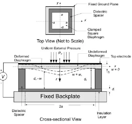
A CMUT is simply a device with two plate-like electrodes biased with a DC voltage and driven
with an additional AC signal to harmonically move one of the plates. The main components are
the cavity, the membrane, and the electrode. Using common integrated circuit (IC) fabrication
processes, a capacitor cell appears as a metallized membrane (top electrode) suspended above
a heavily doped silicon substrate (bottom electrode), typical cross section of a square diaphragm
CMUT is shown in Figure 1-2. An insulating layer is included to prevent the two electrodes from
10
Figure 1-2 CMUT Cross Section
A single transducer element uses many small capacitor cells connected in parallel. Each CMUT
cell is a resonator with a moving membrane suspended over a cavity. The cell size and shape,
membrane topography, and configuration of insulation layers [14], can be modified to optimize
performance parameters, such as output pressure, frequency response, and reliability. A typical
CMUT geometry is built with a square, circular, or hexagonal diaphragm separated from a fixed
backplate by a small airgap.
CMUTs are operated with a dc bias voltage (Vdc) that causes the membranes to deflect
downward to a static operating point. This static operating point determines the sensitivity,
frequency response, and total acoustic output pressure. In transmit mode, an additional ac
voltage is applied to the membrane, which causes the membrane to vibrate around the static
operation point and launches pressure waves into the medium [15] [16].
CMUTs are used both as acoustic transmitters and receivers. On transmit mode, electrostatic
attraction forces are used to put the membranes into vibration by applying an AC voltage.
11
the membranes is twice of the applied frequency. Therefore, a dc bias voltage which is larger
than the ac voltage amplitude is required for proper operation of CMUTs.
The vibration of the membranes generates acoustical waves in the surrounding medium. On
receive mode, harmonic vibration of the membranes, caused by an incident acoustic wave, is
detected using a capacitive detection, which also requires a dc voltage. The vibrations of the
membranes cause a modulation on the overall device capacitance. Under the constant bias
voltage supplied, the capacitance variations result in a current flow in the external electric
circuit which is amplified for further processing.
A control signal operates a switch to enable mode switching from transmit to receive and vice
versa as seen in Figure 1-3. Typically, the diaphragm is created using a microfabricated thin film
conductor such as aluminum or polysilicon or a composite of a non-conducting thin film
structural material such as silicon nitride with a thin coating of a conducting material such as
aluminum or gold on the top is used. Additionally, to avoid electrical breakdown after collapse
due to the pull-in phenomenon, a thin insulation layer, either under the diaphragm conducting
material or on the top of the backplate is used. Finally, a passivation layer on the top of the
diaphragm is used to protect the CMUT from environmental elements [15].
12
1.2.2 Benefits of CMUTs
Piezoelectric materials have dominated the ultrasonic transducer technology. Recently,
capacitive micromachined ultrasonic transducers (CMUTs) have emerged as an alternative
technology offering advantages such as wide bandwidth, ease of fabricating large arrays, and
potential for integration with electronics.
Although the idea of capacitive ultrasound transducers is as old as the early piezoelectric
transducers, piezoelectric materials have dominated ultrasonic transducer technology. The
reason why capacitive transducers have not been popular is that electric field strengths on the
order of a million volts per centimeter (106 V/cm) are required, so that electrostatic forces as
large as a kilo- gram per square centimeter (kg/cm2) would be achieved, as the eminent French
physicist Paul Langevin stated in 1915 [17]. However, recent advances in microfabrication
technology have made it possible to build capacitive ultrasound transducers competing with
piezoelectric transducers. Moreover, CMUTs offer advantages of improved bandwidth ease of
fabrication of large arrays with individual electrical connections, and integration with electronics
[18].
CMUT technology is not simply a low-cost replacement of piezoelectric transducer technology.
Many features inherent in CMUT technology enable revolutionary advances in ultrasound
technology
CMUTs provide many benefits over traditional piezoelectric transducers including improvement
in performance through wide bandwidth, and ease of electronics integration, with the potential
to batch fabricate very large 2D arrays with low-cost and high-yield.
The main differences between piezoelectric transducers and CMUTs can be categorized as
13
Fractional Bandwidth Using piezoelectric devices in some applications is problematic due to the
impedance mismatch between the piezoelectric materials and media; for example in medical
applications , the characteristic impedance of piezoelectric ceramic is (≈ 33 MRayl) is
significantly higher than that of various tissues like blood and fat (≈ 1.6 MRayl). For piezoelectric
transducers, it makes the matching layer difficult to identify, and coupling efficiency poor.
CMUTs offer better acoustic matching to the propagation medium, resulting in broader
fractional bandwidth [19].
Transduction Efficiency For transducer design, one of the most important concerns is efficiency.
Therefore, improved transduction efficiency, boosting both output pressure and reception
sensitivity is required. For CMUTs, higher transduction efficiency can be achieved by increasing
the intensity of electrical field in the CMUT vacuum cavities (high bias voltage). The dielectric
layers in a CMUT can trap surface and interface charges. This trapped charges lead to major
reliability issues; creates voltage drifts. Two major sources of the trapped charges are the
fabrication process and the strong electrical field within the transducer cavities. Different design
schemes are developed currently for CMUTs to overcome this problem (generally complicating
the fabrication process) [20].
Manufacturing Conventional PZT arrays are fabricated by using ”dice and fill” approach, a plate
of piezoelectric material is separated by mechanical dicing and a polymer is infiltrated and cured
within the kerfs. The current limit at element width is 100 µm, and 50 µm for kerf; complicated
manufacturing. The fabrication process of CMUTs is based on standard silicon micromachining
tehniques (or semiconductor fabrication processes).CMUTs have the ability to be integrated
with the front-end electronic circuits on the same wafer. Different from piezoelectric
14
application), the CMUTs are made of thin films which are typically of a thickness ranging from
from submicrometer to a few micrometers [15], [21].
The interest in CMUT research primarily arise from a number of important advantages that
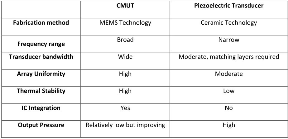
CMUTs enjoy over the piezoelectric counterparts as summarized in Table 1-1
Table 1-1 Comparison of transducers technologies
CMUT Piezoelectric Transducer
Fabrication method MEMS Technology Ceramic Technology
Frequency range Broad Narrow
Transducer bandwidth Wide Moderate, matching layers required
Array Uniformity High Moderate
Thermal Stability High Low
IC Integration Yes No
Output Pressure Relatively low but improving High
1.3
Overview of MEMS fabrication technology.
Most MEMS devices and systems involve some form of lithography-bases microfabrication,
borrowed from the microelectronics industry and enhanced with specialized techniques
generally called ‘’micromachining’’. The major techniques needed to fabricate the non-planar
15
1.3.1 Bulk micromachining
The oldest micromachining technology is bulk micromachining. This technique involves the
selective removal of the substrate material in order to realize miniaturized mechanical
components. Bulk micromachining can be accomplished using chemical or physical means, with
chemical means being far more widely used in the MEMS industry.
A widely used bulk micromachining technique is chemical wet etching, which involves the
immersion of a substrate into a solution of reactive chemical that will etch exposed regions of
the substrate at measurable rates. Chemical wet etching is popular in MEMS because it can
provide a very high etch rate and selectivity. Furthermore, the etch rates and selectivity can be
modified by: altering the chemical composition of the etch solution; adjusting the etch solution
temperature; modifying the dopant concentration of the substrate; and modifying which
crystallographic planes of the substrate are exposed to the etchant solution.
There are two general types of chemical wet etching in bulk micromachining: isotropic wet
etching and anisotropic wet etching. In isotropic wet etching, the etch rate is not dependent on
the crystallographic orientation of the substrate and the etching proceeds in all directions at
equal rates. In theory, lateral etching under the masking layer etches at the same rate as the
etch rate in normal direction. However, in practice lateral etching is usually much slower
without stirring, and consequently isotropic wet etching is almost always performed with
vigorous stirring of the etchant solution, Figure 1-4 shows the isotropic etch process.
Any etching process requires a masking material to be used, with preferably a high selectivity
relative to the substrate material. Common masking materials for isotropic wet silicon etching
include silicon dioxide and silicon nitride. Silicon nitride has a much lower etch rate compared to
16
Figure 1-4 Isotropic etch process
1.3.2 Sputtering
Sputtering is a commercially important technique for thin film deposition. Sputtering is a type of
physical vapor deposition and as such material is transferred directly from a source material
target to the wafer. During sputtering, the source material target is charged to a high negative
potential. It is then bombarded with positively charged ions from argon plasma. The target
material is ejected from the source mainly by momentum transfer from neutral atoms. Ejected
17
maximize the yield of the process, ion energies in the range of 500-3000 volts are used. Due to
the large ion energies present, the deposited material is able to penetrate 1 or 2 atomic layers
into the substrate, producing extremely strong adhesion [22]; Figure 1-5 shows a representation
of this process.
Figure 1-5 Ion Beam Sputtering
1.3.3 Spin coating
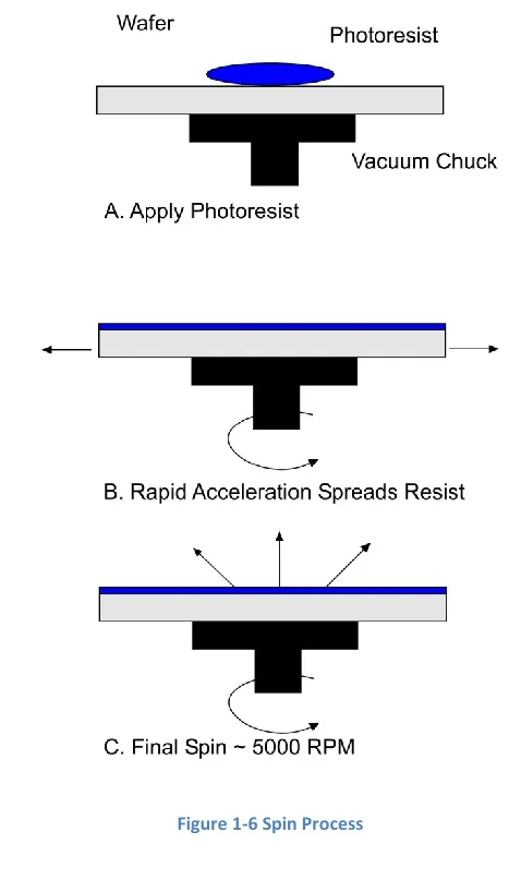
Spin coating is a technique used to apply both temporary materials such as photoresist, and
permanent structural materials. Spinners are found in all microfabrication labs. The spinning
process can be used to deposit viscous materials over wafers without extreme topologies. Due
to poor adhesion between photoresist and metals, phosphosilicate glass (PSG) and polysilicon
and polysilicon, wafers are typically ‘primed’ with Hexamethyl disalazane (HMDS) before the
application of a photoresist. A primed wafer features a hydrophobic surface, which ensures that
surface moisture on the wafer will not interfere with photoresist adhesion.
The priming process begins by baking the wafer. HMDS vapor is applied to create a monolayer
on the wafer surface. An additional benefit of priming the wafers with HMDS prior to the
application of a photoresist is the elimination of the effects of environmental humidity variation,
18
(Figure 1-6 -A) . The spinner then rapidly accelerates to its final spin speed. This evenly spreads
the resist across the wafer surface (Figure 1-6-B). Finally the spinner maintains the final spin
speed for a short interval of time, typically around 1 minute (Figure 1-6-C) to allow the solvent in
the resist to begin evaporating [22].
Figure 1-6 Spin Process
1.3.4 Wafer Bonding
Wafer bonding is a micromachining method that is analogous to welding in the macroscale
world and involves the joining of two (or more) wafers together to create a multi-wafer stack.
19
or anodic bonding; and bonding using an intermediate layer. In general, all bonding methods
require substrates that are very flat, smooth, and clean, in order for the wafer bonding to be
successful and free of voids.
Direct or fusion bonding is typically used to mate two silicon wafers together or alternatively to
mate one silicon wafer to another silicon wafer that has been oxidized. Direct wafer bonding can
be performed on other combinations, such as bare silicon to a silicon wafer with a thin-film of
silicon nitride on the surface as well.
As mentioned, wafer bonding is analogous to welding in the macroscale world. Wafer bonding is
used to attach a thick layer of single crystal silicon onto another wafer. This can be extremely
useful when it is desired to have a thick layer of material for applications requiring appreciable
mass or in applications where the material properties of single crystal silicon are advantageous
over those of thin-film Low Pressure Chemical Vapor Deposition (LPCVD) materials. Direct wafer
bonding is also used to fabricate Silicon-On-Insulator (SOI) wafers having device layers several
microns or more in thickness [22].
Wafer bonding was used in the fabrication of the sensor; an important fact that was considered
is the need of having vacuum in the cavity, since air inside the cavity will cause ionization at a
high electric field that may cause electrical breakdown to cause leakage current [23]; this point
is covered with details in the Chapter 5. Wafer bonded CMUTs have been demonstrated in the
literature, There are a several advantages associated with fabrication of CMUTs by
wafer-bonding technology such as [24]:
- Vacuum cavity formation. Traditionally, the vacuum cavity is formed as follows. First, a
sacrificial layer is deposited and patterned into the membrane shape. Next, the
20
is etched through the membrane to access the sacrificial layer. The sacrificial layer is
removed, and the membrane is released with a wet etch process. The small etch hole is
subsequently sealed under vacuum to create a vacuum sealed gap between the
membrane and the substrate. These steps introduce fabrication limitations to the
traditional process, due to long etch times. With wafer bonding, it is easier and faster to
form a vacuum cavity than it is with the surface micromachining process.
- Cavity Size and Shape. There are three advantages in forming the cavity with the wafer
bonding technique. First, the cavity shape is independent of the membrane shape. The
benefit of this is that one can separately optimize the design parameters (shape, size
and height) of the cavity and membrane without any trade-off between them. Second,
the aspect ratio of the cavity is no longer limited by the height of the sacrificial layer
that can be deposited. Nor is it limited by the slow sacrificial layer etch. Finally, there is
no unwanted material deposition onto the faces of the gap which results in a more
accurate control over the gap height.
- Membrane Size and Shape. Since the CMUT membranes and cavities are fabricated on
different wafers before bonding, the wafer bonding technique provides flexibility to
design CMUTs with membranes of different size, and shape. This is due to the fact that
the membrane is the active layer in the SOI wafer, which can be formed at will,
independent of the cavity size and shape. All this translates into fewer limitations on the
device design when trying to obtain a desired dynamic response.
- Membrane Material. In the wafer-bonding process, the membrane is made from single
crystal silicon, which has desirable mechanical properties, e.g., few internal defects, low
internal mechanical loss, and very low internal stress. This will improve the device
21
as the performance of the device. Lattice defects act as breakage nuclei while lower
internal loss increases the electromechanical coupling efficiency of the device. By using
an SOI wafer to form the membrane, one can achieve a good thickness uniformity
(better than 2.5% of the thickness is commercially available), controllability of the stress
in the membrane, and process repeatability. This is relevant with respect to
commercialization of CMUT fabrication.
Despite the fact that silicon to silicon bonding has been widely used, there are some
disadvantages implied in the process, being one of the most important ones the related to
the high residual stress that will remain in the final product. This residual stress will affect
the final behaviour of the device, modifying its specifications and compromising the
reliability of the system. For that reason a new bonding process has been designed using a
more reliable material, details are presented in Chapter 3 and 5.
1.4
Packaging Techniques
1.4.1 Adhesive Bonding
Adhesive bonding of a die to a package or another die may be accomplished by depositing a film
of epoxy thermoset, acrylic thermoplastic or silicone resins between the layers [25]. Although
the thermal and electrical conductivity of this technique are inferior to other methods of
mounting, by loading the adhesive material with silver particles the electrical and thermal
conductivities of the bond can be controlled over a wide range. Adhesive bonding is a low-cost
technique that lends itself easily to automation. Additional cost savings can be obtained since
metal plating on bonding surfaces is unnecessary. Due to the plastics used, a low curing
22
subject to voids. Due to the elastic properties of the bonding material, the stress in the die is
reduced. The material can also be removed to allow rework of the device if necessary. Due to
the nature of the bonding materials used, these devices are not suitable for use in harsh
environments. Adhesive bonding is used for the non-planar CMUT array design due to the ease
of integrating a large number of dies into a single package.
1.4.2 Wirebonding
Wirebonding uses thin wires to connect bond pads on the die to the packaging interconnects.
The attachment process uses a combination of heat, pressure and ultrasonic energy. The result
of the bonding is a weld consisting of either electron sharing or diffusion of atoms at the bond
site. Pressure during the bonding ensures intimate contact between the wire and the pad, as
well as helping to break up any oxide layer or contamination present at the interface. The
presence of ultrasonic energy during the bond further increases the ability to break up the oxide
or contaminants. The use of heat accelerates the process of atomic diffusion, reducing the
amount of time necessary to form a connection [26]. The wirebonding process was used to
make the connections between CMUTs in the non-planar array.
1.5
Specific Research Objectives
– To design a non-planar CMUT array for automotive collision avoidance using the theory
developed in [13].
– Determine non-planar geometry suitable for fabrication using state of- the-art MEMS
fabrication techniques.
– Determine sensor geometry.
– Detailed sensor design.
23
– Behaviour simulation of the sensor geometry using 3-D finite element analysis method.
– Design verification by comparing analytical results with FEA results.
– To develop a fabrication process to implement the non-planar sensor microarray.
– Fabrication and testing of the microarray.
1.6
Principle Results
The principle results of this research work have been summarized as follows:-
1. The theory developed by [13] has been used to design capacitive micromachined
ultrasonic transducer based non-planar micro array. The non-planar array was designed
to work at 40 kHz targeted to be used for automotive collision avoidance.
2. The design is a 5x5 array having 5 sensing surfaces along each x and y axis, with 7
different elevation levels. The array side length and height is 8.55 mm and 3.36 mm
respectively. The beamwidth is 40° with maximum sidelobe intensity of -10dB.
3. A new analytical model has been developed to accurately obtain the capacitance change
and load deflection profile of a square clamped diaphragm. This model incorporates the
effect of biasing voltage, external pressure, fringing field and large deflections.
4. The mathematical model has been verified by comparing it with 3-D
Theromoelectromechanical IntelliSuite™ based FEA to verify the results with excellent
agreement.
5. A new fabrication process has been developed using for the first time BCB
(Benzocyclobutene) as the isolation layer in the CMUT. A packaging process has been
developed using VeroWhitePlus Fullcure835 (Plastic) to realize the non-planar structure,
24
As a result of this work, the following paper has been published:
Journal Publication:
M. Rahman, J. Hernandez and S. Chowdhury, "An improved analytical method to design CMUTs
with square diaphragms," Ultrasonics, Ferroelectrics and Frequency Control, IEEE Transactions
on, vol. 60, no. 4, pp. 834, 845, April 2013.
Conference Publication:
J. Hernandez Aguirre, T. Zure and S. Chowdhury, "Capacitance Measurements of an SOI Based
CMUT," in LASCAS 2013, 2013 IEEE 4th Latin American Symposium on Circuits and Systems,
Cusco, 2013.
T. Zure, J. Hernandez, S. Chowdhury,” Dynamic Analysis of an SOl based CMUT”, Proc. Of IEEE
International Conference on Industrial Technology (ICIT), 2012, 19-21 March 2012, Athens, pp.
539 - 544.
1.7
Thesis Organization
Chapter 2 deals with introducing the fundamentals of array based beamforming covered in
previous work [13]. The basic theory behind and the mathematical model for designing discrete
hyperbolic paraboloid is presented. The physical parameters of the array have been evaluated
using the existing theory.
Chapter 3 deals with the design and simulation of the CMUT. Since the CMUTs work on the basic
principle of capacitance change due to a diaphragm deflection, a novel and easy to implement
25
diaphragm deflection profile. This model incorporates the effects of biasing voltage, fringing
field capacitance, external pressure, diaphragm geometry, also accounts for the contribution of
the dielectric properties of the diaphragm structural material and also the insulation layer used
on the bottom electrode to prevent electrical break down and material properties. The final
specifications of the sensor are presented.
Chapter 4 present the validation of the parameters of the sensor by comparing them with FEA
simulations performed using IntellisuiteTM showing excellent agreement. A easy to implement
Simulink model is presented to model the dynamic behaviour of the sensor.
Chapter 5 covers the fabrication and packaging process of the sensor, the materials used,
various fabrication steps and the involved recipes are provided. The conceptual, simulation and
actual photographs at various stages have also been provided. A basic set up for testing the
sensor has been designed showing excellent results.
Chapter 6 makes the concluding remarks, discussions and future scope of in this specific
26
2
CHAPTER 2
MODELING OF NON-PLANAR CMUT ARRAY
A non-planar array refers to a one or two dimensional array where the sensor elements are
distributed at different elevations along the vertical axis. By constructing a non-planar array
geometry a better array response over a desired frequency range will be obtained as compared
to planar geometries [27]. In this chapter the theory to determine the specifications of the
non-planar CMUT array for the collision avoidance application has been presented. The
theory needed to design the non-planar array is presented first, and then the desired
specifications for the array are presented to find the final dimensions of the array.
27
2.1.1
Beamforming
Beamforming or spatial filtering is a signal processing technique used in sensor arrays for
directional signal transmission or reception [28]. This is achieved by combining elements in
a phased array in such a way that signals at particular angles experience
constructive interference while others experience destructive interference. Beamforming can be
used at both the transmitting and receiving ends in order to achieve spatial selectivity.
It has it has been established [29] that a macroscale continuous aperture acoustical sensor
having the shape of a hyperbolic paraboloid surface as shown in Figure 2-1Error! Reference
source not found. can provide a constant beamwidth directional response without any
microelectronics based signal processing.
Practically, the beamwidth should remain constant from a value governed by the physical size of
the array up to the Nyquist frequency. Thus, the lateral dimensions of the array in x and y axis
can be determined from the lowest operating frequency whereas the beamwidth is
independently specified in each axis by the amount of out of- plane twist present at the array
extremities [29].
28
A square footprint hyperbolic paraboloid surface can be expressed in cartesian coordinate as:
L x y
z tan 2
(2.1)Equation L x y
z tan 2
(2.1) Equation 2-3Where x , y and z are the Cartesian coordinates, L is the sidelength in x or y direction, and α is
the amount of out of- plane twist in the z direction at the surface extremity ( Error! Reference
ource not found.).
Figure 2-2 Out of plane twist angle α in a Hyperbolic Paraboloid
The far-field directional response, or array factor, of a continuous aperture hyperbolic
paraboloid-shaped acoustical sensor of side length L in a given direction (θ, ɸ) as referenced
from the array normal is expressed as [29]:
29 where:
1 tan tan
1
2
2
n (2.5)
Equation t an t an 1
1
2
2
n
(2.5
)
assumes that out-of-the-plane angle α is small and the sensor sidelength L is expressed inunits of wavelengths of the desired acoustical frequency
.
In [29] it has been shown that the array has a reasonably constant directional response value
for large values of 1/2αL with a small out-of-plane twist angle α. However, the array response
calculated following t an t an 1
1
2
2
n
(2.5
)
is valid only if the out of the plane angle α is less than or equal to 10°.The intrinsic beamforming capability of this geometry is highly desirable for use in a microarray
to minimize system power consumption and cost, while taking advantage of the scaling benefits
offered by microfabrication. Due to that the current microfabrication techniques are basically
planar processes that involve successive deposition, patterning and etching of thin films, a
continuous aperture hyperbolic paraboloid geometry transducer array cannot be fabricate using
the current microfabrication techniques. To overcome this obstacle, a discretized hyperbolic
paraboloid geometry transducer array has been suggested in the literature [13].
This discretized array can provide an intrinsic constant beamwidth beamforming capability that
can match very closely with that from a continuous aperture hyperbolic paraboloid geometry
transducer. To obtain a discretized version, the double integral in t an t an 1 1
2
2
n
(2.5
)
has been expressed as the sum of an infinite number of discrete points separated byinfinitesimal intervals using standard spatial sampling techniques, such as the Riemann
30
to a finite one of an arbitrary number of levels. Out of the various Riemann Summation
techniques available, center based Riemann Summation was used in this case as it is good for
non-monotonic functions and its ability to calculate error bands. Following [13], the
center-based Riemann summation in one dimension can be expressed as:
b a
dx x
f
n in
a
b
n
a
b
i
a
f
12
1
(2.6)Where n represents the number of discretization levels. The maximum error given for this
approximation is:
2
2
312n a b M A dx x f b a mid
(2.7)where,
M
2 is the maximum value of andA
mid is the value of at the midpoint ofthe interval a-b.
Applying b a dx x f
n in
a
b
n
a
b
i
a
f
12
1
(2.6
)
to 2 2 2 2 2 tan tan 2 2 1 , L L L L L xy y x n j dydx e L f (2.4
)
twice, first along x axis and then along y axis, the array factor for the discretized array can be
derived as [13]:
1 0 1 0 2 tan tan 2 ' ' ' '1
,
M m N n L y x y x t je
MN
f
(2.8)31
M
L
m
L
x
2
1
2
' ,
N
L
n
L
y
2
1
2
' (2.9)and M and N are the number of sensing surfaces in the x and y directions respectively.
2.1.2
Array Sidelength Determination
The minimum sidelength S of the square footprint discretized hyperbolic paraboloid geometry
sensor array can be determined from the following relation [13]:
lower
f
Kc
S
min
(2.10)Where
c
is the speed of sound in media and is the lower bound frequency in theoperating range. is the fitting parameter based on the amount of acceptable beam shape
variation.
As the beamwidth decreases with an increase in the frequency, empirical parameter K maintains
the beamwidth within a range of variations for all the frequencies in a frequency range
of . The Table 2-1 list some of the values of K for different acceptable
beamwidth variation:
Table 2-1 Beamwidth Control Parameter K Values
K (Unitless) Beamwidth variation (˚)
3 7
32
8 2
10 1
2.1.3
Number of Sensing Surfaces Determination
Using the following equations we can specify the number of sensing surfaces per axis for a
square footprint array for -10dB and -6 dB respectively [12], [13]:
5
.
69
0
.
8637
,
5695 . 0 uppers
X
N
M
(2.11)
1
.
49
0
.
8484
,
9029 . 0 uppers
X
N
M
(2.12)2.1.4
Array Height
The height of the array is directly related to the out of plane twist present at the array
extremities. The maximum height measured from the center of a continuous aperture
hyperbolic paraboloid geometry array can be determined from the out of plane twist angle α as , where S is the sidelength of the array. The next figure shows the relation in a graphical
form:
33
It is known that the height has a small reduction due to the sampling point is occurring
at the center of the outermost sensing surface as is shown in the
Figure 2-4.
Figure 2-4 Discrete Array Height Sampling
However this sampling error introduces an angular error of less than 4.0% for arrays with more
than 5 sensing surfaces per axis. This affects the beamwidth by less than [13].
The total height for a discretized square footprint array geometry can be determined using the
following equation [12]:
10
3762
.
0
5215
.
0
M
0.792S
H
(2.13)where M represents the number of sensing surfaces in each x and y axis.
Using the theory discussed before the non-planar array was fabricated on a microfabricated
tiered geometry that can approximate a discretized hyperbolic paraboloid surface as shown in
34
Figure 2-5 A graphical representation of the discretization process of a hyperbolic paraboloid geometry
2.2
Model Validation
It has been presented the needed theory to design a non-planar array, in order to validate it and
show its scope different plots are presented. Since the wavelength of the work frequency
dictate the length of the array, different beamwidth can be obtained by changing the length of
the array, the following figures were plotted using a frequency of 40 KHz and changing the
length of the array to show how this idea.
35
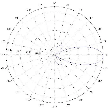
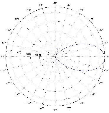
Figure 2-7 Beam shape, array length 1.8 lambda
36
Figure 2-9 Beam shape, array length 2.5 lambda
It can be seen that by changing the length of the array different beamwidth can be obtained,
this point shows the flexibility of the non-planar array. It is clear that the length and height of
the array is dictated by the working frequency. Shows some dimensions for different
frequencies:
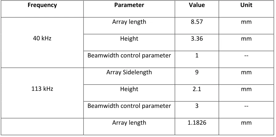
Table 2-2 Non-planar array dimensions for different working parameters
Frequency Parameter Value Unit
40 kHz
Array length 8.57 mm
Height 3.36 mm
Beamwidth control parameter 1 --
113 kHz
Array Sidelength 9 mm
Height 2.1 mm
Beamwidth control parameter 3 --
37
2.3 MHz Height 402.1 µm
Beamwidth control parameter 8 --
2.3
Design Methodology Non-Planar Array
In order to have ultrasound technologies and ultrasonic sensors used in automotive occupancy
sensor (AOS) system such as the collision avoidance system some requirements need to be
meet:
The selected ultrasonic frequency and pressure levels should not affect humans or be
heard by household pets that are likely to ride along in a vehicle equipped with an
ultrasonic system.
Natural and artificial sound sources encountered during vehicle usage should not
interfere with the acoustic echo.
Ultrasound frequencies should be chosen to minimize signal attenuation in the media
and maximize reflection from the target to allow a large signal to noise ratio (SNR)
enabling accurate classification.
Hearing range data for many species was evaluated as well as human exposure limits. Cats and
mice have some of the highest known hearing frequencies at 91 kHz and 100 kHz respectively.
Despite this fact it has been demonstrated that such animals are not disturbed by those
frequencies. Ultrasonic energy guidelines are defined separately for air-coupled and contact