University of South Carolina
Scholar Commons
Theses and Dissertations
2017
Integrating Nano-Patterned Ferromagnetic and
Ferroelectric Materials For Smart Tunable
Microwave Applications
Tengxing Wang
University of South Carolina
Follow this and additional works at:https://scholarcommons.sc.edu/etd
Part of theElectrical and Computer Engineering Commons
This Open Access Dissertation is brought to you by Scholar Commons. It has been accepted for inclusion in Theses and Dissertations by an authorized administrator of Scholar Commons. For more information, please [email protected].
Recommended Citation
Wang, T.(2017).Integrating Nano-Patterned Ferromagnetic and Ferroelectric Materials For Smart Tunable Microwave Applications.
INTEGRATING NANO-PATTERNED FERROMAGNETIC AND FERROELECTRIC MATERIALS FOR SMART TUNABLE
MICROWAVE APPLICATIONS
by
Tengxing Wang
Bachelor of Science
Tianjin University of China 2010 Master of Science
Fudan University of China 2012
Submitted in Partial Fulfillment of the Requirements
for the Degree of Doctor of Philosophy in
Electrical Engineering
College of Engineering and Computing
University of South Carolina
2017
Accepted by:
Guoan Wang, Major Professor
Mohammod Ali, Committee Member
Grigory Simin, Committee Member
Chen Li, Committee Member
c
Dedication
Acknowledgments
The four-year Ph.D. experience in the University of South Carolina is a hard but
valuable journey. It is absolutely a milestone in my life, and an important starting
point for my future career. During my Ph.D., I received all kinds of help from people
around me, and I couldn’t have finished this dissertation without the support from
them. It is my great pleasure to acknowledge them for their guidance, assistance and
company.
Foremost, I would like to express my most sincere gratitude to my adviser Dr.
Guoan Wang. I’m still feeling grateful that four years ago Dr. Wang gave me the
opportunity to participate in his research group and become a member of SMART
Lab. It is really my great fortune to meet Dr. Wang and research under the guidance
of Dr. Wang. His inspiring ideas, broad scientific knowledge, and deep technology
insight impress me all the time, and lead me in all the way of my research work.
Dr. Wang gives me sufficient freedom in my research to work with the topics I’m
interested in, and when I have any issues, he is always there to help, and he is
always able to propose smart and efficient methods to tackle the issues. Absolutely
Dr. Wang is one of the smartest and nicest people I’ve ever met. In my opinion, in
addition to scientific research, what I have learned most from Dr. Wang is the attitude
towards the science and life. Dr. Wang is full of positive and optimistic attitude, and
that power always influences me and encourages me against frustrations and failures.
What I have learned and gained from Dr. Wang is invaluable, and I could not have
imagined having a better adviser.
Chen Li for their valuable time and effort serving in my Ph.D. committee and for
their brilliant, constructive and precious suggestions in the proposal defense and
dissertation. I’m very grateful to the scientists in Center for Nanoscale Materials,
Argonne National Laboratory: Dr. Ralu Divan, Dr. Leonidas Ocola and Mr. Daniel
Rosenmann, for supporting me with the research and fabrication in the clean room.
Without their involvement and efforts, I could not have finished my fabrication and
research.
I am indebted to my colleagues and friends in the SMART Lab: Yujia Peng, Wei
Jiang, B M Farid Rahman and Yong Mao Huang, for stimulating research discussions,
for the great help in simulation, fabrication and measurement, and for all the progress
we have made together under the guidance of Dr. Guoan Wang. I also want to thank
my office mates: Wuzhao Yan, Zhichao Liu, Zheqing Zhou, Lixing Yang, Guangxing
Niu and Shijie Tang, for their friendship and company. Because of them, my Ph.D.
life is rich, colorful, and memorable.
Most importantly, I would like to express my eternal love and appreciation to
my beloved wife, Chunling (Penny) Wang. If there are three things in the world
that I love most, they are sun, moon and you. Sun for days, moon for nights, and
you forever. I always think the most fortunate thing in my life is meeting you and
marrying you. I always appreciate your selfless sacrifice and great efforts for our
family. I always feel happy because of your everlasting love, company, and unlimited
support. It is you and your endless love that grant me the power to go through every
hard period, and make me believe there is always hope, just because I will always
fight for you and will never ever let you down. Thank you and I will always love you.
I would like to express my gratitude and love to my parents: Lijun Wang and
Guanghui Li. Thank you very much for your endless love, unlimited support and
Abstract
The wireless communication market has been ever-growing in the recent decades.
Radios with high performance and capabilities to support wireless connections are
increasingly demanded. Recent developments in wireless communications targeting
ubiquitous connections have resulted in ever more complex system structures for
supporting multiple frequency bands and standards. Reconfigurable and tunable
RF/microwave technologies have the potential to significantly simplify the systems.
The main objective of this dissertation is to develop tunable technologies and
design concepts, and propose a new design methodology to implement dually
electrically tunable microwave components by integrating both selectively patterned
ferromagnetic and ferroelectric materials.
The first part of the dissertation demonstrates the concept and topology of
selectively patterned ferromagnetic (Permalloy) thin film enabled electrical tunability.
The properties of Permalloy are demonstrated in details, and electrically tuning
mechanism and topology are introduced and analyzed with both magnetic simulation
and measurement results. By integrating selectively patterned Permalloy thin film to
the coplanar waveguide transmission line, electrically tunable microwave transmission
line is achieved. The inductance density of tunable transmission line can be
electrically tuned by dc current, and the feasibility of Permalloy enabled electrical
tunability is proved. To further validate the efficacy and utilize the topology to design
tunable microwave components, tunable inductors and a tunable bandpass filter are
designed and fabricated. For the tunable inductors, a planar spiral inductor and a 3-D
to enable the tunability, and more than 10% inductance tunability has been achieved.
Design principle of the tunable bandpass filter is then analyzed and demonstrated,
and by integrating Permalloy thin film, the center frequency can be continuously
tuned by dc current.
Based on the topology of Permalloy enabled electrical tunability, the second part
of the dissertation proposes and demonstrates the methodology of ferromagnetic
(Permalloy) and ferroelectric (PZT) enabled dual tunability for electrically tunable
microwave applications. The tunable microwave components have both inductive and
capacitive tunability by simultaneously integrating Permalloy and PZT thin films.
To validate the efficacy and prove the concept, two dually electrically tunable phase
shifters are implemented, including a slow wave transmission line phase shifter and
a 3-D lumped-element phase shifter, and the performance can be tuned by applying
dc current and/or dc voltage. Compared with planar transmission line phase shifter,
3-D structure has significant higher tuning efficiency and more compact size, and thus
the maximal length normalized phase tunability has reached to 210◦/cm. The dual
tunability enabled by Permalloy and PZT not only improves the design flexibility
and electrical tuning range, but also, more importantly, realizes the capability
of characteristic impedance retaining, by which when microwave components are
tuned, the characteristic impedance can be kept constant. This design concept
and methodology can be further developed and applied to implement other tunable
Table of Contents
Dedication . . . iii
Acknowledgments . . . iv
Abstract . . . vi
List of Tables . . . xi
List of Figures . . . xii
Chapter 1 Introduction . . . 1
1.1 Motivation . . . 1
1.2 Tuning Technologies Overview . . . 4
1.3 Research Objective and Dissertation Overview . . . 14
Chapter 2 Permalloy and Permalloy Enabled Tunable Microwave Transmission Line . . . 19
2.1 Classification of Magnetism . . . 20
2.2 Ferromagnetic Materials . . . 24
2.3 Py Enabled Electrically Tunable Transmission Line . . . 35
2.4 Improvement of Tunability Utilizing Py Lamination Structure . . . . 44
Chapter 3 Permalloy Thin Film Enabled Electrically
Tunable Inductors . . . 47
3.1 Introduction . . . 47
3.2 Tunable Spiral Inductor . . . 48
3.3 Tunable Solenoid Inductor . . . 55
3.4 Couclusoin . . . 63
Chapter 4 Permalloy Thin Film Enabled Electrically Tunable Bandpass Filter . . . 65
4.1 Introduction . . . 65
4.2 EBG-CPW Cell and Resonator . . . 65
4.3 Design of Patterned Py Thin Film Enabled Tunable Bandpass Filter 71 4.4 Measurement Results and Discussion . . . 72
4.5 Conclusion . . . 73
Chapter 5 Electrically Tunable Microwave Components with Dual Tunability. . . 75
5.1 Introduction . . . 75
5.2 Fundamentals of Ferroelectric Materials . . . 76
5.3 Principle of Dual Tunability and Characteristic Impedance Retaining 80 5.4 Electrically Tunable Slow Wave Transmission Line Phase Shifter . . . 81
5.5 3-D Lumped Element Electrically Tunable Phase Shifter . . . 89
5.6 Conclusion . . . 99
Chapter 6 Summary and Future Work . . . 101
6.2 Future Work . . . 103
List of Tables
Table 1.1 Comparison of Typical Tunable Technologies [13, 36, 37] . . . 14
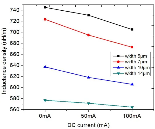
Table 2.1 Inductance density of tunable CPW transmission line at 4 GHz. . 42
Table 2.2 Inductance density of CPW transmission lines at 4 GHz with different line widths under different dc current. . . 43
Table 3.1 Summary of Inductance at 2.2 GHZ. . . 51
Table 3.2 Summary of Q Factor at 2.2 GHz. . . 51
Table 3.3 Summary of Measurement Results at 2 GHz. . . 59
Table 5.1 Summary of Measurement Results of Transmission Lines at 2 GHz. 84 Table 5.2 Summary of Extracted Measured Transmission Line Parameters. . 86
Table 5.3 Comparison of Tunable Phase Shifter with State of Art. . . 88
Table 5.4 Summary of Phase Shift at 2 GHz. . . 95
List of Figures
Figure 1.1 Modern mobile handsets can support multiple frequency bands
and wireless standards [3]. . . 2
Figure 1.2 System architecture of a RF subsystem with multiple frequency
bands diversity [4]. . . 3
Figure 1.3 A concept implementation of tunable RF front-end. . . 4
Figure 1.4 Tunable BPF proposed in [10]: (a) schematic and (b) optical
photo. . . 6
Figure 1.5 Switchable notch UWB tunable BPF in [11]. . . 6
Figure 1.6 Tunable reflection-type phase shifter in [12]: (a) schematic and
(b) optical photo. . . 7
Figure 1.7 MEMS enabled tunable inductor presented in [14]: (a)
schematic and (b) SEM photo. . . 8
Figure 1.8 MEMS enabled tunable capacitor [15]: cross-section view (left)
and top-down SEM photo (right). . . 8
Figure 1.9 MEMS enabled tunable BPF [16]: (a) SEM photo and (b)
optical photo. . . 9
Figure 1.10 SEM image of switchable interdigital filter proposed in [17]. . . . 9
Figure 1.11 Optical image of the Ka-band tunable BPF presented in [22]. . . 10
Figure 1.12 Side view (left) and top view (right) of tunable patch antenna
using BST as substrate [23]. . . 11
Figure 1.13 Layout of proposed tunable meander line phase shifter in [33]
with YIG as substrate. . . 12
Figure 1.15 Solenoid transformer with laminated Permalloy as magnetic core [35]: (a) top view, (b) schematic of cross-section of transformer layout and (c) illustration of transformer with
interleaved coils. . . 13
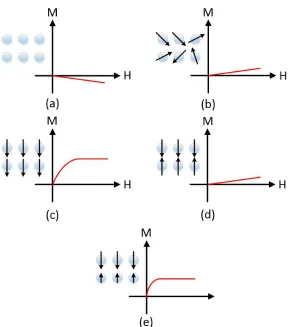
Figure 2.1 Magnetic moments ordering and M−H relation of (a) Diamagnetism, (b) Paramagnetism, (c) Ferromagnetism, (d) Antiferromagnetism and (e) Ferrimagnetism. . . 23
Figure 2.2 Shape anisotropy constant in a prolate spheroid of Co as a function of aspect ratio [47]. . . 26
Figure 2.3 Magnetic field around a prolate spheroid [47]. . . 27
Figure 2.4 Structure of a 180◦ domain wall [39]. . . 28
Figure 2.5 Hysteresis loop for a ferromagnetic [47]. . . 29
Figure 2.6 Hysteretic loops for two idealized magnetization cases: (a) hard−axis and (b) easy−axis magnetization process [48]. . . 30
Figure 2.7 Comparison of different ferromagnetic materials regarding to coercivity and relative permeability [54]. . . 32
Figure 2.8 Simulated hysteresis loop of patterned Py thin film along easy axis and hard axis. . . 33
Figure 2.9 Optical photo of (a) fabricated patterned Py enabled tunable transmission line, (b) Py pattern on transmission line 1 with long edge parallel to the signal line and (c) Py pattern on transmission line 2 with long edge perpendicular to the signal line. 37 Figure 2.10 Measurement results of inductance density of transmission line without Py, with parallel and with perpendicular orientation of Py patterns, respectively. . . 37
Figure 2.11 Simulation results of real part of Py pattern susceptibility versus frequency under different external biasing magnetic field (left) and correlated magnetization orientation of the Py pattern (right). . . 39
Figure 2.13 Schematic of electrically tuning mechanism utilizing dc current. . 40
Figure 2.14 Schematic of measurement setup. . . 41
Figure 2.15 Measurement results regarding to the tunable transmission line
inductance density versus frequency under different dc current. . . 42
Figure 2.16 Measured inductance density of tunable CPW transmission
lines with various widths. . . 43
Figure 2.17 Simulated susceptibility of single layer and lamination structure. . 44
Figure 3.1 Optical photo of tunable octagon spiral inductor (left) and
micro-patterned Py thin film (right). . . 48
Figure 3.2 Measurement setup and the DUT on probe station (DC current and RF signal are provided simultaneously between input and
output ports of tunable inductors). . . 50
Figure 3.3 Measurement result of inductance with 100 nm Py thin film. . . . 52
Figure 3.4 Measurement result of inductance with 200 nm Py thin film. . . . 52
Figure 3.5 Measurement result of Q factor. . . 53
Figure 3.6 (a) Schematic of 3-D tunable solenoid inductor and (b)
magnified partial view. . . 57
Figure 3.7 Surface micro-machining process of 3-D tunable solenoid inductor. 58
Figure 3.8 Measurement results of inductance at different frequency under
different dc current. . . 60
Figure 3.9 Measurement results of Q factor at different frequency under
different dc current. . . 60
Figure 3.10 Measured results regarding to the insertion loss comparison of
solenoid inductor with and without Py thin film. . . 61
Figure 4.1 Schematic of EBG-CPW cell (left) and equivalent circuit model
(right). . . 66
Figure 4.3 Simulation results of EBG-CPW cell and equivalent circuit model. 68
Figure 4.4 Simulation results of EBG-CPW resonator and equivalent
circuit model. . . 68
Figure 4.5 Simulation result of resonant frequency of EBG-CPW resonator
versus signal line inductance. . . 69
Figure 4.6 Simulation result of resonant frequency of EBG-CPW resonator
versus gap capacitance. . . 70
Figure 4.7 Optical photo of tunable BPF composed of two EBG-CPW
resonators, and SEM photo of Py pattern. . . 71
Figure 4.8 Measurement result of tunable BPF under different dc biasing
current. . . 73
Figure 5.1 Permittivity versus temperature and phase transition of
ferroelectrics [101]. . . 77
Figure 5.2 Polarization versus electrical field for (a) normal dielectrics, (b) ferroelectric phase when T<Tc and (c) paraelectric phase when
T>Tc [101]. . . 77
Figure 5.3 Perovskite crystal with (a) symmetrical structure exhibiting no spontaneous polarization and (b) unsymmetrical structure
showing spontaneous polarization [103]. . . 78
Figure 5.4 SEM photo of (a) fabricated slow wave CPW structure, (b) zoom-in view of PZT thin film between signal line and ground,
and (c) patterned Py thin film. . . 82
Figure 5.5 Surface micro-machining process of SI-CPW slow wave
transmission line. . . 83
Figure 5.6 Measurement results of (a) insertion loss and (b) Q factor of
the group of transmission lines with different configurations. . . . 85
Figure 5.7 Measured phase shift of the implemented regular and thin films enabled SI-CPW slow wave transmission lines, respectively,
Figure 5.8 Schematic of Py and PZT enabled tunable phase shifter and magnified view of MIM capacitor. The inset on the upper left
is the optical photo of fabricated phase shifter under the probes. . 90
Figure 5.9 Lumped elements equivalent circuit of tunable phase shifter. . . . 90
Figure 5.10 (a) SEM photo of PZT enabled MIM capacitor and (b)
extracted relative permittivity of PZT thin film. . . 92
Figure 5.11 Phase shift comparison among measurement, simulation and
theoretical calculation without dc bias. . . 94
Figure 5.12 Measurement results of phase shift of the device versus
frequency under different dc biasing conditions. . . 95
Figure 5.13 Measurement results of equivalent characteristic impedance and phase shift of the device versus frequency under different dc
biasing conditions. . . 97
Figure 5.14 Measurement results of insertion loss at different frequency
Chapter 1
Introduction
1.1 Motivation
The fast growing wireless communication market has seen dramatic changes in both
requirements and capabilities of the radios to support wireless connections. Recent
developments in wireless communications have resulted in the radios that have
evolved from a single-mode, triple-band 2G system to a triple-mode, 9-band (4×GSM,
5×UMTS with HSPA+) high-speed data-capable system in year 2010. The trend of
mobile devices targeting ubiquitous connection continues, and a fast growing number
of frequency bands are required to be supported. As the fourth generation (4G)
long-term evolution (LTE) systems are rapidly deployed, the number of frequency
bands listed in the current LTE specifications has reached to 40, with the operation
frequency ranging from 0.7 GHz to 3.8 GHz [1, 2].
Modern wireless communication systems are required to support multiple
frequency bands. Furthermore, integrating multi-functional modules into a single
wireless device to operate over different standards has become a defined trend. Such
demands in the market put critical requirements on the performances of the wireless
systems, including higher functionality, more compact size, longer battery life, and
more importantly, lower cost. Figure 1.1 illustrates such a scenario that a modern
cellphone is compatible with several wireless standards, including 3G, 4G, GPS,
Bluetooth, WiFi, etc.
Figure 1.1: Modern mobile handsets can support multiple frequency bands and wireless standards [3].
increase in cost offers obvious benefits to the end users, while it raises significant
challenges to the system designers and manufactures, especially for today’s even
more complex wireless communication systems. Figure 1.2 depicts the system
architecture of a highly integrated RF transceiver subsystem, which is compatible
with HSDPA/WCDMA/EDGE standards [4]. Parallel integration is utilized and
separate RF front-ends are stacked to support different frequency bands and wireless
standards. Large die area is required for the architecture, and even larger area is
needed for the off-chip passive components, such as filters, duplexers, and switches.
To realize true wireless ubiquity and meet the challenge of high integration,
technological innovations from both system level and device level are highly
demanded. On the system level, concepts such as software defined radio (SDR) and
Figure 1.2: System architecture of a RF subsystem with multiple frequency bands diversity [4].
are exploited to adapt hardware parameters to the requested working frequencies and
wireless standards. Apparently, in Figure 1.2, if the parallel integration of static filters
can be replaced by several tunable filters to support different operation frequency
bands, the RF subsystem can be significantly simplified. A concept implementation
of tunable RF system is illustrated in Figure 1.3. Tunable matching network and
tunable bandpass filters are utilized instead of the parallel integration of static RF
components, and the complexity of the system is significantly reduced.
Figure 1.3: A concept implementation of tunable RF front-end.
importance to achieve miniaturized, frequency-agile and multifunctional systems. In
order to realize tunable microwave devices, special tuning elements and techniques are
required to be used and integrated into the device circuitry. Great efforts have been
made to develop tunable microwave components with traditional technologies. Each
of these tuning techniques has its own advantages and limitations. The main purpose
of this dissertation is to propose a novel methodology for the implementation of
electrically tunable microwave components, utilizing the advantages of conventional
techniques, and overcoming some of the limitations. Before the description of the
proposed design methodology, a general overview and comparison of different tuning
technologies is delivered in the next section.
1.2 Tuning Technologies Overview
Extensive tuning technologies have been developed, such as conventional mechanical
tuning elements (piezoelectric transducers/actuators), semiconductor varactors (PIN
diodes and GaAs Schottky diodes), as well as newer technologies, such as
microelectromechanical systems (MEMS). In addition, special functional materials
implementing tunable microwave components.
1.2.1
Mechanically Tunable Techniques
Mechanically tunable technique utilizing piezoelectric transducers or actuators is a
relatively early technology to realize tunability. The tuning mechanism is generally
shifting a material or tuning screws to affect the resonant frequency or coupling
effect of different structures in microwave devices. As presented in [6–8], piezoelectric
transducers/actuators are used. Dielectric slab can be either moved vertically above
a RF filter, or used to generate deformation on a conductive film to tune the dielectric
resonator filters or evanescent-mode cavity filters. The mechanical tuning techniques
can provide high-Q and high power-handling capabilities. However, the bulky size
of tunable components raises the integration issue, and the low tuning speed (∼ms)
greatly limits the utilization in the microwave range.
1.2.2
Semiconductor Varactors
Semiconductor varactors are popular elecments used for tuning, including PIN diodes
and GaAs Schottky diodes. The capacitance of a varactor varies as a function of
reverse voltage applied across its p-n junction. Basically, the working mechanism
of a varactor is based on altering the effective thickness of the depletion region of
the junction under a reverse DC voltage, which is equivalently similar to changing
the distance of two plates of a capacitor to tune the capacitance. The capacitance
is generally inversely proportional to the thickness of depletion zone, while the
thickness of depletion region is proportional to the square root of applied voltage.
Therefore, the variability of capacitance is inversely proportional to the square root
of applied DC voltage [9]. The advantages enabling the popularity of semiconductor
varactors are their availability, low cost, high tuning range, and low response
(a) (b)
Figure 1.4: Tunable BPF proposed in [10]: (a) schematic and (b) optical photo.
Figure 1.5: Switchable notch UWB tunable BPF in [11].
components to realize tunability. For example, in [10] as shown in Figure 1.4,
semiconductor varactors are placed at various internal nodes of a bandpass filter
to adjust the transmission poles and compensate the coupling strength, so that the
center frequency and bandwidth of the filter can be tunable. In [11] shown in Figure
1.5, semiconductor varactors are embedded to the electromagnetic bandgap (EBG)
of a notch filter, to control the connection and disconnection of main EBG unit
cell and additional capacitive structures. The size of the EBG unit cell is therefore
(a) (b)
Figure 1.6: Tunable reflection-type phase shifter in [12]: (a) schematic and (b) optical photo.
is tunable. Semiconductor varactors are used in [12] and incorporated into the
impedance-transforming quadrature coupler, which can be seen in Figure 1.6, so
that a tunable reflection-type phase shifter is implemented. The major limitations
of semiconductor varactors are low quality factor, low power handling capability and
low linearity, and PIN diodes consumes some DC power. Moreover, the introduction
of semiconductor varactors brings in complicated biasing network and other auxiliary
components as well, such as biasing pads, DC block capacitors, RF choke inductors,
etc. The varactors and biasing network not only require large area, but also increase
the complexity of systems.
1.2.3
RF MEMS Technology
RF MEMS, as an important class of technology, has been successfully applied in
tunable RF device topologies. In general, RF MEMS devices enable the micrometer
level movement of beams or patches to obtain a switching function or a variable
capacitance controlled by applied DC voltage. Low loss is an important merit of
RF MEMS devices (∼0.05-0.2 dB in the frequency range of 1-100 GHz for MEMS
switches [13]), and they also have high linearity, low power consumption, high
capability of power handling, and high isolation (MEMS switches).
(a) (b)
Figure 1.7: MEMS enabled tunable inductor presented in [14]: (a) schematic and (b) SEM photo.
Figure 1.8: MEMS enabled tunable capacitor [15]: cross-section view (left) and top-down SEM photo (right).
in designing tunable microwave components. For example, in [14], RF MEMS
technology is used to achieve a tunable inductor with high tuning range and Q factor.
The tunability of inductance is enabled by switching the mutual inductance between
primary coil and different secondary coils. Figure 1.7 shows the implementation.
Yonghyun Shimet al.[15] reported a high-Q tunable MEMS capacitor, which is shown
in Figure 1.8, with more than 6:1 tunability using multimetal surface micromachining
process. The capacitance can be changed by adjusting the deformation of the hexagon
patch controlled by DC voltage. Based on the proposed tunable RF MEMS capacitor,
(a) (b)
Figure 1.9: MEMS enabled tunable BPF [16]: (a) SEM photo and (b) optical photo.
Figure 1.10: SEM image of switchable interdigital filter proposed in [17].
with continuous electrostatic tunability by using three tunable capacitor bands, each
consisting of one continuously tunable capacitor and three switched capacitors. Figure
1.9 shows the SEM photo and optical photo. Another tunable RF MEMS bandpass
filter is reported in [17], as shown in Figure 1.10, and the pass band can be tuned by
switching on and off different resonators enabled by MEMS cantilevers.
The limitations of MEMS technology include high response time (∼µs),
complicated fabrication and low reliability. Additionally, since MEMS switches can
only be switched between the status of on and off, it can only introduce discontinuous
Figure 1.11: Optical image of the Ka-band tunable BPF presented in [22].
1.2.4
Ferroelectric Materials
In addition to the technologies illustrated above, ferroelectric is another category
of materials which is also attractive and extensively explored. Barium Strontium
Titanate (BST) and Lead Zirconate Titanate (PZT) are among various kinds of
ferroelectric materials and have been widely utilized for many microwave applications
requiring frequency agility, phase shifting, harmonic generation, or pulse shaping,
such as fast tunable delay lines, filters and matching networks, and other electronically
reconfigurable architectures [18]. The utility is enabled by the transverse piezoelectric
effect and the ability to tune the ferroelectric materials’ permittivity with an
applied electric field. Therefore, voltage controlled varactors can be constructed by
sandwiching a ferroelectric thin film between two metallic electrodes.
BST enabled varactors have been commonly used to control the frequency and/or
phase response of various devices [19–23]. For example, in [22], a quasi-elliptic
coplanar waveguide tunable bandpass filter operating at Ka-band enabled by
BST varactors, shown in Figure 1.11, is reported, and utilizing the epitaxial
BST-on-sapphire technology, anU-band filter is for the first time introduced. Yelong
Figure 1.12: Side view (left) and top view (right) of tunable patch antenna using BST as substrate [23].
the schematic of the device. BST layer is used as substrate of the antenna, and the
permittivity of substrate can be tuned by applying DC voltage between metal patch
and ground such that the resonant frequency of the antenna is varied accordingly.
Similar to BST, PZT is another ferroelectric material, and is also widely used for
implementing tunable microwave components [24–26].
The main advantages of ferroelectric enabling the popular applications are high
and tunable permittivity, low response time (∼ns), and continuous variation of
permittivity with the tuning electric field. However, material loss, non-linearity
and temperature sensitivity are particular limitations for ferroelectric materials. For
most designs, the tuning method is generally limited to DC voltage, which is lack of
flexibility.
1.2.5
Ferromagnetic Materials
In recent years, ferromagnetic materials have attracted great attention for their
Figure 1.13: Layout of proposed tunable meander line phase shifter in [33] with YIG as substrate.
Figure 1.14: Sketch of tunable solenoid inductor with FeNi as magnetic core [34].
The tunable nature of ferromagnetic arises from the adjustable permeability subject
to an external biasing magnetic field. Different kinds of ferromagnetic are extensively
explored and various tunable microwave components have been developed and
realized [27–35].
In [33], Yttrium-Iron-Garnet (YIG) crystal is used as substrate and a tunable
phase shifter is reported, which is shown in Figure 1.13. When external biasing
magnetic field is provided, the permeability of YIG substrate can be changed and
the phase shift is accordingly tuned. However, along with the variation of phase
shift, due to the permeability change of substrate, the characteristic impedance of
the device is also changed. Marina Vroubel et al. reported an electrically tunable
Figure 1.15: Solenoid transformer with laminated Permalloy as magnetic core [35]: (a) top view, (b) schematic of cross-section of transformer layout and (c) illustration of transformer with interleaved coils.
sketch of the device and operation principle. A static magnetic field can be generated
when DC current is applied to the solenoid winding. The static magnetic field is
oriented parallel to the hard axis of NiFe and change the permeability of magnetic
core, resulting in the inductance variety of solenoid inductor. However, due to the
bulk utilization of ferromagnetic, the operation frequency of solenoid inductor is
limited by the natural ferromagnetic resonant (FMR) frequency, and the tunable
inductor can work only below 1 GHz. In [35], Permalloy layers are inserted into
coils of transformers. Figure 1.15 illustrates the device. Due to high permeability of
Permalloy, the inductance of primary and secondary coils is greatly increased, and
the coupling factor is significantly improved.
Overall, high permeability is a primary advantage of ferromagnetic materials,
especially the permeability can be continuously tuned by biasing magnetic field.
Table 1.1: Comparison of Typical Tunable Technologies [13, 36, 37]
Tuning
Technology Mech.
1 YIG PIN
diode Varactor diode BST RF MEMS Unloaded
Q >1000 >500 Rs=1-4 Ω 30-50
2 30-1502 50-400
Tuning
Speed >10µs ns ns ns ns µs
Bias >100 V N/A 10-400
mA <30 V <30 V 20-100 V Linearity
(IIP3: dBm)
high <30 >33 10-35 10-35 >60
Power
Handling high 2 W ∼mW ∼mW ∼mW 1-2 W
Power
Consumption high high medium low negligible negligible
Size large large small small small small
Cost high high low low low medium
Integration difficult difficult good good good good
Mechanical1 At 10 GHz2
ferromagnetic materials in designing microwave components. Moreover, for most
tunable implementations enabled by ferromagnetic materials, external magnetic
biasing field is required, which apparently introduces the integration issue.
1.3 Research Objective and Dissertation Overview
Table 1.1 summarizes the performance comparison among different tunable
technologies reviewed in the previous section. Obviously, each of the existing tunable
technologies has different advantages and limitations. The choosing is strongly
depended on the particular system specifications.
Following the motivation and literature review demonstrated in the previous
sections, the primary objective of this research is to use the advantages of conventional
techniques and solve some of the limitations, and develop a new solution for tunable
introduced and a novel methodology is proposed for implementing fully electrically
tunable microwave components by integrating both selectively patterned Permalloy
and PZT thin films. To fully illustrate the design methodology and validate the
efficacy, the research is divided into three primary parts, and accordingly four main
chapters are incorporated in the dissertation to deliver detailed description.
•Part I: Demonstrate the concept and topology of selectively patterned Permalloy
thin film enabled electrical tunability
In Chapter 2, the idea of Permalloy thin film enabled electrical tunability is
presented and tunable microwave transmission line is implemented utilizing this
design topology. First, the ferromagnetic properties of Permalloy is presented
in detail, and the working principle of selectively patterning Permalloy thin film
to increase ferromagnetic resonant (FMR) frequency is theoretically analyzed and
validated with magnetic simulation results. The selectively patterned Permalloy thin
film is deposited on top of the signal line of coplanar waveguide (CPW) transmission
line, and the performance of different orientations of thin film pattern parallel and
perpendicular to the signal line is then compared and discussed respectively with
measurement results. Permalloy thin film is integrated into conventional transmission
line as a part of signal line, and thus no extra area or components is introduced.
Instead of conventional tuning method utilizing external biasing magnetic field, DC
current is applied between the two ports of CPW transmission line to generate
static magnetic field for tuning the permeability of Permalloy thin film pattern [38].
The permeability variation of Permalloy thin film results in the tunability of signal
line inductance density, and the electrically tunable transmission line is achieved.
The detailed electrically tuning mechanism is illustrated. The tunability is strongly
dependent on the tuning static magnetic field, while the magnetic field intensity
is related to both the amount of DC current and signal line width. A group of
analyze and demonstrate this effect. To improve the performance, new configuration
of Permalloy thin film is theoretically explored and lamination structure is proved to
be effective to increase the tunability.
• Part II: Validate the topology efficacy of patterned Permalloy thin film enabled
electrical tunability for tunable microwave devices
Part I introduces the topology of Permalloy enabled electrical tunability. To
prove the feasibility of this design method, in Chapter 3, patterned Permalloy thin
film is successfully utilized in implementing electrically tunable inductors. Exploiting
the high and tunable permeability, Permalloy thin film is at first integrated with
spiral inductors to improve the performance and achieve tunability. The inductance
and quality factor (Q factor) are significantly enhanced compared with regular spiral
inductor without Permalloy, and the inductance can be tuned by DC current. Due
to the selective patterning of Permalloy thin film, the operation frequency of tunable
inductor reaches to several GHz. The performance of tunable spiral inductors with
different thickness of Permalloy thin film is analyzed and discussed to provide clues
for future optimization and improvement. In addition to the tunable spiral inductor,
Permalloy thin film is then used to achieve a tunable 3-D solenoid inductor. Special
configuration is adopted and patterned Permalloy thin film is used as magnetic
core of solenoid inductor. Compared with the distribution of static magnetic field
surrounding a metal wire generated by DC current, the magnetic field inside the
solenoid winding is more uniform to tuned the permeability of Permalloy thin film.
Therefore, compared to tunable spiral inductor, 3-D solenoid inductor more effectively
use the DC current for tuning and larger tunability is achieved.
Chapter 4 proposes a prototype implementation of tunable bandpass filter
(BPF) utilizing the concept of Permalloy enabled tunable transmission line, and
further validates the efficacy of this design topology. The BPF is constructed with
film is nano-patterned with e-beam (electro-beam) lithography to improve the FMR
frequency and support the operation frequency of BPF. The center frequency of the
BPF can be tuned when DC current is applied between input and output ports.
• Part III: Demonstrate the methodology of Permalloy and PZT enabled dual
tunability for fully electrically tunable microwave applications
Part I and Part II of the research comprehensively demonstrate and validate
the topology of Permalloy enabled electrical tunability. In Part III, a new design
methodology integrating both Permalloy and PZT are demonstrated and validated for
designing tunable microwave components. Permalloy introduces inductive tunability
and PZT is capable of realizing capacitive tunability. By combining both inductive
and capacitive tunability, the concept of dual electrical tunability is introduced
and achieved. Chapter 5 demonstrates the dual tunability and dual tunability
enabled characteristic impedance retaining capability, with several tunable microwave
components implemented as validation.
This chapter is divided into two sections. The first section demonstrates a step
impedance coplanar waveguide (SI-CPW) slow wave transmission line. Patterned
Permalloy thin film is deposited on top of the high impedance sections of signal line
to improve the inductance density, while PZT thin film is deposited into the gap
between low impedance sections of signal line and ground to increase the capacitance
density. The integration of Permalloy and PZT thin film not only enhances the
performance, but also enables dual tunability of SI-CPW transmission line. When
DC current and DC voltage are provided, the electrical length of transmission line
can be inductively and capacitively tuned simultaneously, and equivalently the phase
shift can be tuned. The dual tunability enabled characteristic impedance retaining
capability is introduced and proved in this section.
Section two proposes a 3-D lumped elements electrically tunable phase shifter.
shifter, and PZT thin film enabled tunable metal-insulator-metal (MIM) is introduced
in stead of PZT gap capacitance utilized in the SI-CPW slow wave transmission line to
increase the capacitance and reduce the tuning DC voltage. Compared with SI-CPW
phase shifter, due to the utilization of optimized 3-D structure, significantly larger
electrical tunability is achieved with much lower tuning DC current and DC voltage.
The phase shift can be tuned electrically while the equivalent characteristic impedance
is kept constant by selectively applying DC current and DC voltage, and the efficacy
of characteristic impedance retaining is further validated.
As demonstrated above, the main body of research is presented in Chapter 2,
3, 4 and 5. The dissertation is concluded in Chapter 6. The author’s work is
summarized and contributions are itemized in this chapter. Future work of research
Chapter 2
Permalloy and Permalloy Enabled Tunable
Microwave Transmission Line
In Chapter 1, a general overview on microwave tunable techniques has been
introduced. State-of-art tuning technologies including mechanical methods,
semiconductor varactors, RF MEMS, ferroelectric and ferromagnetic materials and
their utilization in the realizations of tunable microwave applications have been
discussed and presented. Advantages and limitations of different tunable technologies
are compared and analyzed. As demonstrated before, the main purpose of this
dissertation is proposing a new design methodology to implement electrically tunable
microwave components by integrating both ferromagnetic and ferroelectric materials,
and achieve smart tunable microwave applications with dual electrical tunability.
In literature review of the previous chapter, for most conventional tunable designs
exploiting ferromagnetic materials, external biasing magnetic field is required for
tuning, which apparently results in the integration issue. Therefore, before realizing
dual electrical tunability, electrically tuning ferromagnetic materials must be achieved
first. This chapter demonstrates the utilization of Permalloy, a kind of ferromagnetic
material with good properties, and the operation mechanism of electrically tuning
of Permalloy. Based on that, Permalloy enabled electrically tunable microwave
transmission line is implemented.
This chapter begins with the introduction of classification of magnetism
discussed and presented. The working principle of Permalloy enabled electrical
tunability is analyzed and demonstrated afterwards and utilizing the results of
theoretical discussion and analysis, electrically tunable microwave transmission line
is implemented.
2.1 Classification of Magnetism
The phenomenon of magnetism can be presented macroscopically and
microscopically [39, 40]. In macroscopical, materials react attractively or repulsively
when they are exposed to other materials. In microscopical, magnetism is mainly
due to the electrons of the atom, which have a magnetic moment originating from
their motion. Even though nucleus also has a small magnetic moment, it is negligible
compared with that of the electrons, and it has insignificant effect to the gross
magnetic properties. For electrons, there are two kinds of motions, spin and orbital,
and correspondingly two magnetic moments are associated with them, which are
spin magnetic moment and orbital magnetic moment, respectively. In materials,
atoms contain many electrons, and each electron spins about its own axis and moves
along its own orbit. Since the magnetic moments associated with the two kinds of
motions are vector quantity, the magnetic moment of the atom is the total vector
sum of all its electronic moments. Accordingly, two possibilities can be raised and
five kinds of magnetism can be classified:
1. The magnetic moments of all the electrons are oriented in a way that they
cancel out each other, and the atom as a whole has no net magnetic moment. This
mechanism results in diamagnetism.
2. The magnetic moments of all the electrons are partially canceled and the atom
is left with a net magnetic moment, which is referred to as magnetic atom. This leads
Diamagnetism
Diamagnetism is a kind of very weak magnetism form. When no external biasing
magnetic field is applied, there is no net magnetic moment in atoms of diamagnetic
substances. However, when magnetic field is provided, the magnetization is produced,
which is oriented in the opposite direction of the external magnetic field, and
is strengthened as the increasing of biasing magnetic field. The susceptibility of
diamagnetic materials, which is defined as the variation in magnetization with
respect to the applied magnetic field, is small and negative, and is independent of
temperature. The typical diamagnetic materials include He, Au and Cu.
Paramagnetism
Compared with diamagnetism, paramagnetic materials are composed of atoms or
ions which have a net magnetic moment due to non-cancellation of the spin and
orbital components. The coupling between magnetic moments are weak, so their
alignment is random as a result of thermal energy. When external magnetic field is
applied, the magnetic moments are aligned toward the same direction as magnetic
field. However, due to the relatively small external magnetic field energy compared
to thermal energy, only a small fraction of magnetic moments can be aligned so as
to strengthen the practical field and magnetization. Therefore, the susceptibility
of paramagnetic materials is positive and small. Moreover, the susceptibility is
temperature dependent. When the temperature is increased, the thermal agitation
enhances the randomization of magnetic moments alignment, resulting the variation
Ferromagnetism
Ferromagnetism is one of the strongest forms of magnetism. The most important
characteristic property of ferromagnetic materials is spontaneous magnetization,
resulting from the alignment of the magnetic moments located on an atomic lattice.
The magnetization tends to lie along easy directions that are decided by crystal
structure, atomic-scale texture or sample shape, even though external magnetic field
is absent. The quantum mechanics can be described by Heisenberg model, which
demonstrates the parallel alignment of magnetic moments introduced by exchange
interaction between adjacent moments. The parallel alignment of the magnetic
moments in ferromagnetic materials results in a strong internal magnetic field, and
the susceptibility of ferromagnetic materials are positive and very large, as high as
106. The common ferromagnetic materials are Fe, Ni and Co.
Antiferromagnetism
Antiferromagnetism is different from ferromagnetism particularly in the manner
of spin alignment. In antiferromagnetic materials, the exchange interaction
between neighboring atoms results in anti-parallel alignment magnetic moments,
and the magnetic moments with opposite direction cancel each other, showing
no net magnetization as paramagnetic materials. Therefore, the susceptibility of
antiferromagnetic materials is positive and very small. Some common materials of
antiferromagnetism are Cr, FeO and MnO.
Ferrimagnetism
Ferrimagnetism is another kind of magnetic ordering. In terms of magnetic
moments alignment resulted from exchange interaction, ferrimagnetism is similar
Figure 2.1: Magnetic moments ordering and M−H relation of (a) Diamagnetism, (b) Paramagnetism, (c) Ferromagnetism, (d) Antiferromagnetism and (e) Ferrimagnetism.
the anti-parallel aligned magnetic moments do not cancel each other so that the net
magnetization is not zero in the materials. Therefore, ferrimagnetic materials behave
similarly to ferromagnetic materials, except that the susceptibility is much lower.
One of the most commonly used ferrimagnetic materials is Fe3O4. Other examples
include MnZn and NiZn.
According to the ordering of magnetic moments, ferromagnetic, antiferromagnetic
and ferrimagnetic materials are called magnetically ordered materials, while
diamagnetic and paramagnetic materials are non-magnetically ordered due to the
fact that no ordering in magnetic moments exists without the presence of applied
orderings and M−H relations of five types of magnetism.
2.2 Ferromagnetic Materials
During the last decades, ferromagnetic materials have been greatly explored and
developed, and become one of the most widely used materials among all kinds of
magnetic materials because of their potential in a wide range of applications [41–44].
2.2.1
Fundamental Concepts
Some of the fundamental concepts and properties of ferromagnetic materials, such as
magnetic energy, domain, hysteresis, and ferromagnetic resonance (FMR) frequency,
are introduced as following.
Magnetic Energies
In magnetic materials, the most important energy is the exchange energy, which can
be denoted asEex. The exchange energy illustrates the exchange interactions between
two neighboring electrons, and as demonstrated before, those interactions contribute
to parallel aligning adjacent atomic magnetic moments in the ferromagnetic materials,
resulting in an internal magnetic field even without external applied magnetic field.
The exchange interaction can be explained by Coulomb repulsion and Pauli exclusion
principle, which sate that two electrons can not occupy the same quantum state
within a quantum system. In a atomic system with many electrons, the total energy
is denoted by Exchange Hamiltonian [45, 46]:
Eex =H=−2
X
i6=j
JijSi·Sj (2.1)
whereSi andSj are the sum of all the atoms pairs on lattice sites i and j, respectively.
Jij is the exchange integral between Si and Sj. When only nearest neighboring
If J < 0, equation 2.1 indicates antiferromagnetic interaction, which antiparallel
aligns the two spins in the antiferromagnetic materials. WhenJ is a positive value, it
describes ferromagnetic materials, in which ferromagnetic interaction tends to parallel
align two spins.
Another important type of magnetic energy is anisotropy energy Ea, which
illustrates the phenomenon that magnetic moments tend to be aligned along
the easy axis of the ferromagnetic materials. There are several kinds of
anisotropy [39], including magnetocrystalline anisotropy, shape anisotropy, stress
anisotropy, exchange anisotropy and anisotropy induced by process such as magnetic
annealing, plastic deformation and irradiation. Among those anisotropy, only
magnetocrystalline anisotropy is the intrinsic property of materials. Then, strictly,
all the others are extrinsic or induced.
The magnetocrystalline anisotropy originates from the crystal−field interaction
and spin−orbit coupling, or other inter-atomic dipole-dipole interaction [40]. When
external magnetic field is applied trying to reorient the spin of an electron, the orbit of
the electron tends to be reoriented as well due to the spin-orbital coupling. However,
the orbit is strongly coupled to the crystal lattice and resists the attempt to rotate
the spin axis. Then the magnetocrystalline anisotropy is defined as energy required
to rotate the spin system of a domain away from the easy axis to the hard axis, which
is also the energy to overcome the spin-orbit coupling. The expression for this energy
is different according to the symmetries of materials. For a ferromagnetic material
with uniaxial anisotropy, the magnetocrystalline anisotropy can be expressed as:
Ea=Ku1sin2θ+Ku2sin4θ+Ku3sin6θ+· · · (2.2)
where Kun are the anisotropy constants, θ is the angle between magnetization
direction and easy axis.
The anisotropy can also be originated due to the shape of ferromagnetic samples,
Figure 2.2: Shape anisotropy constant in a prolate spheroid of Co as a function of aspect ratio [47].
dissertation. If the shape of the ferromagnetic sample is spherical, the same applied
magnetic field can magnetize the sample to the same extent in every direction.
However, when the shape of the sample is non-spherical, magnetizing the sample along
its long axis is easier than along a short axis, which is because the demagnetization
field along the long axis is smaller than that along the short axis. Increasing the
aspect ratio of sample can effectively increase the shape anisotropy energy. Figure
2.2 illustrates the shape anisotropy constant of Co as a function of aspect ratio. In
our research in this dissertation, the ferromagnetic material is selectively patterned
to increase the aspect ratio, so that the shape anisotropy is enhanced and the high
frequency performance of the ferromagnetic materials is improved, which will be
demonstrate in the following sections.
The magnetostatic energy Ems is a type of magnetic energy generated by the
demagnetization field in the sample [39]. Figure 2.3 illustrates the formation
Figure 2.3: Magnetic field around a prolate spheroid [47].
an applied magnetic field, and a north pole and a south pole are generated at the two
ends of the prolate spheroid, respectively. The magnetic field lines radiate from the
north pole to the south pole outside the sample, while the magnetic field inside the
sample is oppositely oriented, which tends to demagnetize the sample, and is called
demagnetization field. The magnetostatic energy thus can be expressed, based on
demagnetization field, as [39]:
Ems=− 1 2
Z
Hd·M dv (2.3)
whereHdis the demagnetization field, andM is the magnetization field of the sample.
Accurately evaluating the distribution of Hd is difficult, and the demagnetization
factor is introduced to calculate Hd:
Hd=−NdM (2.4)
where Nd is the demagnetization factor and it is a tensor strongly dependent on the
shape of the magnetic sample. The detailed calculation methods can be referenced
in [39].
For a magnetic sample, when an external biasing magnetic filed is provided, the
Zeeman energyEz is generated, which can be described as:
Ez =−µ0
Z
Happ·M dv (2.5)
where Happ is the applied magnetic field, and M is the local magnetization. The
Figure 2.4: Structure of a 180◦ domain wall [39].
The final magnetization state and properties of the ferromagnetic sample is
determined by the minimization of the sum of those energies described above.
Domain
Ferromagnetic materials have internal magnetic field due to the spontaneous
alignment and magnetization, even in the absence of an applied magnetic field.
However, the net magnetization of ferromagnetic materials as a whole is zero in the
demagnetized state. The reason is that ferromagnetic material in the demagnetized
state is divided into domains, within each of which all the magnetic moments
are parallel aligned to each other. The boundaries between domains are domain
walls, across which the direction of magnetic moments alignment gradually changes
to a different one. Figure 2.4 illustrates the structure of a domain wall. When
ferromagnetic materials are in the demagnetized state, the orientation of magnetic
moments in domains are with such different directions that they can cancel each other,
and therefore the net magnetization is zero. The direction along which the magnetic
Figure 2.5: Hysteresis loop for a ferromagnetic [47].
the easy axis is hard axis. The easy axis indicates the direction of magnetic moments
alignment which enables the domain in the lowest energy level, and the formation of
domain structures contributes to minimize the total magnetic energy of ferromagnetic
materials.
Hysteresis
Another phenomenon of ferromagnetic materials is the nonlinear magnetization
behavior subject to an external magnetic field, and the magnetization curve is usually
a hysteretic loop, which is demonstrated in Figure 2.5.
In the initial unmagnetized state, domains are oriented randomly so that the
net magnetization is zero. When an external field is applied, the domains, of which
the magnetization direction is similar to the external magnetic field, begin to grow,
causing domain wall movement, while other domains with unfavorable magnetization
orientation are shrunk. As the applied magnetic field is increased in the positive
direction, the magnetic induction follows the curve from 0 to Bs and eventually the
magnetization is saturated and saturation induction Bs is reached, where all the
domain walls in the ferromagnetic materials are eliminated and a single domain is
Figure 2.6: Hysteretic loops for two idealized magnetization cases: (a) hard−axis and (b) easy−axis magnetization process [48].
continues to increase along with H, due to B = H = 4πM. The curve of B from
demagnetized state to saturation induction Bs is called the normal induction curve.
After the saturation, when applied magnetic field H is reduced to zero, the
magnetic induction drops from Bs to Br, which is called residual induction. The
reason of the generation of residual induction is that domain walls are unable to fully
reverse their motions back to the original positions even in the absence of external
magnetic field. When the applied magnetic field is reduced in the negative direction,
the magnetic induction is decreased to zero, where the required magnetic field is called
coercivity (Hc). The coercivity is related to the hysteretic loss. A smaller coercivity
value can introduce lower hysteretic loss.
When the reversed external magnetic field is further increased, the reverse
saturation (−Bs) is achieve. The loop traced out from −Bs to Bs is called the
major hysteresis loop, and the loop is inversely symmetric about the origin.
The smaller loop inside the major hysteresis loop in Figure 2.5 is called minor
hysteresis loop, which illustrates the case when initial magnetization is interrupted
(for example, at point a shown in the figure) and magnetic field H is reversed.
Generally, magnetization processes along easy axis and hard axis are different [48],
which show different appearances of hysterestic loops. For uniaxial ferromagnetic
materials, a purely hard−axis magnetization process involves rotation movement of
in a linear magnetization−magnetic field (M−H) loop. An easy−axis magnetization
is related to domain wall movement in a direction that grows the favorably oriented
domain. Figure 2.6 demonstrates the two idealized magnetization processes along
hard axis and easy axis, respectively.
Ferromagnetic Resonant Frequency
The phenomenon of ferromagnetic resonant (FMR) was firstly observed in 1946 by
Griffiths [49] and the theory was developed by Kittel in 1948 [50]. When a microwave
signal is applied to a ferromagnetic sample and the sample is subject to a static
magnetic filed, the magnetic moments precesses about the direction of the applied
static magnetic field, and the microwave power is strongly absorbed if the frequency of
the microwave transverse field is equal to the precessional frequency of the magnetic
moments. In the absence of damping, the equation of motion can be expressed as [45]:
dM/dt=γ(M ×B0) (2.6)
where M is magnetization of the ferromagnetic sample, γ is the gyromagnetic ratio,
andB0is the applied static magnetic field. The magnetization precesses at the Larmor
frequency fL = ω0/2π, where ω0 =γB0. The magnetization of the ferromagnetic is
mainly due to the spin moments of the electrons, so the gyromagnetic ratio(γ) can be
expressed as γ = −(e/me), where me is the mass of an electron. The applied static
magnetic field is usually replaced by the effective field Hef f, which takes anisotropy
field into consideration, and Equation 2.6 can then be revised as:
dM/dt =γ(M ×Bef f) (2.7)
Based on Equation 2.7, the famous Kittel’s equation can be derived [45, 50] and
used to estimate the FMR frequency:
ω02 = γ
2
Figure 2.7: Comparison of different ferromagnetic materials regarding to coercivity and relative permeability [54].
where H0 is the applied static magnetic field, Hani is the anisotropy field, and Ms is
the saturation magnetization; Nx,Ny and Nz are demagnetization factors along x, y
and z direction, respectively. Some special cases are:
• Sphere: Nx =Ny =Nz = 13, and then ω0 = 2γπH0;
• Thin film with static magnetic field perpendicular to the plane: Nx =Ny = 0,
Nz = 1, and then ω0 = 2γπ(H0−Hani4πMs);
• Thin film with static magnetic field in plane: Ny =Nz = 0, Nx = 1, and then
ω0 = 2γπ[H0+Hani4πMs)](1/2)
2.2.2
Permalloy Thin Film
Among all kinds of ferromagnetic materials, Permalloy (Py) has been extensively
explored and developed. Py is composed of 80% of Nickel (Ni) and 20% of Iron
(Fe), and has good ferromagnetic properties such as large and tunable permeability,
small magnetostriction, low coercivity, and no stress anisotropy [51–53]. Figure 2.7
demonstrates the comparison of Py with other ferromagnetic materials regarding to
Figure 2.8: Simulated hysteresis loop of patterned Py thin film along easy axis and hard axis.
ferromagnetic materials, Py has larger relative permeability and smaller coercivity.
The hysteresis loss of ferromagnetic materials is highly related to coercivity, and
small coercivity can contribute to reduce the magnetic hysteresis loss. According
to previous demonstration and Figure 2.6, magnetization along the hard axis of
ferromagnetic materials has smaller coercivity than easy axis magnetization. To
theoretically show the different hysteresis loop and coercivity of Py along easy and
hard axis, magnetic simulation using Object Oriented Micromagnetic Framework
(OOMMF) [55] is conducted. 50 nm thick Py thin film is patterned as a slim bar with
the length of 2 µm and width of 200 nm. In this dissertation, standard parameters
for Py (gyromagnetic ratio γ=2.8 GHz/kOe, exchange constant A = 13× 10−12
Jm−1, damping constant α=0.015, and anisotropy constant K
U=0) are used in all
the magnetic simulation with OOMMF. Figure 2.8 shows the simulation results. It
is clearly shown that compared with easy axis magnetization, the coercivity of hard
axis magnetization is negligible. In this dissertation, the external biasing magnetic
field is always parallel to the hard axis of the Py pattern to reduce the hysteresis loss.
tuning of permeability of Py thin film, which will be demonstrated in the following
section.
FMR frequency is a key factor of ferromagnetic material and it indicates
the operation frequency limitation of utilizing Py in designing tunable microwave
components. Py shows high and tunable permeability only when the working
frequency is below FMR frequency, and if the working frequency exceeds the FMR
frequency, the permeability becomes very low and even negative. However, the FMR
frequency of un-patterned Py thin film is usually below 1 GHz, which apparently
limits the utilization of Py on the microwave frequency range. The method to
improve FMR frequency is indicated in Equation 2.8 by increasing the anisotropy
fieldHani. According to previous introduction, anisotropy field is composed of several
kinds of anisotropy, among which, magnetocrystalline anisotropy is determined by the
crystalline structure of ferromagnetic materials and is the intrinsic property. Shape
anisotropy is determined by the geometry of ferromagnetic materials and can be easily
introduced. One of the common strategies to improve shape anisotropy is selectively
patterning, which is the main strategy adopted in this dissertation. The Py thin
film is elongated and patterned as slim rectangle bars to increase aspect ratio. As
demonstrated before, demagnetization energy along the long axis is weaker than that
along the short axis. Thus, by properly patterning Py thin film, high built-in shape
anisotropy is introduced, and the total anisotropy field of Py thin film is improved
so that the FMR frequency is increased consequently. According to our preliminary
research [56], e-beam (electron-beam) lithography is employed to selectively pattern
the Py thin film with the dimensions of 440 nm width and 10 µm length, and the
FMR frequency of above 4.5 GHz is achieved. To obtain higher FMR frequency,
larger aspect ratio is required to increase shape anisotropy field. E-beam lithography
technique is optimized and the width of Py pattern is reduced to 150 nm with the
The method utilized to deposit Py thin film is DC magnetron sputtering, which is
performed with Lesker CMS 18 system. Py thin film is deposited at room temperature
in a 2.1 mT Argon (Ar) gas atmosphere. The substrate is rotated at 20 rpm and Py
is sputtered by the accelerated Ar+ ions and the deposition rate is controlled to be
0.023 nm/s. During the deposition, no extra magnetic field is provided. To increase
the adhesion between Py and substrate, Chromium or Titanium of 5−10 nm thick
thin film is deposited first with e-beam evaporation system as adhesion layer.
2.3 Py Enabled Electrically Tunable Transmission Line
As demonstrated before, Py has large relative permeability and the permeability can
be tuned by applying magnetic field. The large and tunable permeability widely
enables Py in tunable microwave applications [34, 35, 58–63]. Among all the tunable
applications, tunable transmission line is the fundamental element to construct other
tunable microwave components. This section introduces the mechanism, properties,
and implementation of Py enabled tunable coplanar waveguide (CPW) transmission
line.
2.3.1
Orientation Analysis of Patterned Py Thin Film
Py thin film has large relative permeability. When Py thin film is integrated with
transmission line, the inductance density (L) of transmission line can be significantly
improved. However, the domain structure of Py thin film must be well-controlled to
introduce good permeability performance. According to [64] and [65], possible domain
patterns of ferromagnetic slim bars are either 180◦domain or multi-domain structures,
depending on the balance of anisotropy energies. The 180◦ domain pattern, with the
magnetization oriented parallel to the direction of the anisotropy axis without an
external magnetic field applied, is suitable for radio frequency application, especially
![Fig ur e1 .1 :Mo de r n mo bileha nds e t sc a n s uppo r tmult iplef r e q ue nc yba ndsa ndw ir e le s s s t a nda r ds [3 ].](https://thumb-us.123doks.com/thumbv2/123dok_us/8393919.1385587/19.612.95.514.109.364/fig-mo-bileha-uppo-tmult-iplef-ndsa-nda.webp)
![Fig ur e1 .2 : Sy s t e m a r c hit e c t ur ediv e r s it yo f aR F s ubs y s t e m w it h mult iplef r e q ue nc yba nds[4 ].](https://thumb-us.123doks.com/thumbv2/123dok_us/8393919.1385587/20.612.91.525.73.458/fig-sy-ediv-ubs-mult-iplef-yba-nds.webp)
![Fig ur e 1 .5 : Sw it c ha ble no t c h UWBt una ble B P F in [1 1 ].](https://thumb-us.123doks.com/thumbv2/123dok_us/8393919.1385587/23.612.100.520.71.282/fig-sw-it-ble-uwbt-una-ble-in.webp)
![Fig ur e1 .1 2 : SideB STv ie w( le f t )a nd t o p v ie w( r ig ht )o f t una blepa t c h a nt e nnaus inga s s ubs t r a t e [2 3 ].](https://thumb-us.123doks.com/thumbv2/123dok_us/8393919.1385587/28.612.113.498.75.284/fig-sideb-stv-una-blepa-nnaus-inga-ubs.webp)
![Fig ur e1 .1 5 : So le no id t r a ns f o r me r w it h la mina t e d P e r ma llo y( a ) t o p v ie w , ( b) s c he ma t ic o f c r o s s - s e c t io n o f t r a ns f o r me r la y o ut a nd ( c ) illus t r a t io na s ma g ne t icc o r e[3 5 ]:o f t r a ns f o r me r w it h int e r le a v e d c o ils .](https://thumb-us.123doks.com/thumbv2/123dok_us/8393919.1385587/30.612.144.479.72.325/fig-mina-llo-ns-illus-icc-int-ils.webp)
![Fig ur e2 .2 : Sha pea s pe c t r a t ioa nis o t r o pyc o ns t a nt in apr o la t es phe r o id o f C oa s af unc t io n o f[4 7 ].](https://thumb-us.123doks.com/thumbv2/123dok_us/8393919.1385587/43.612.182.427.73.324/fig-sha-pea-ioa-nis-pyc-apr-phe.webp)
![Fig ur e 2 .4 : St r uc t ur e o f a1 8 0◦ do ma in w a ll [3 9 ].](https://thumb-us.123doks.com/thumbv2/123dok_us/8393919.1385587/45.612.148.466.69.286/fig-ur-st-uc-ur-do-in-ll.webp)