IJEDR1502018
International Journal of Engineering Development and Research (www.ijedr.org)89
A Wireless Protected Nonstaop Data Transmission
among Authenticated Portable Storage Devices
through GSM Network
1
Dipali Shende , 2Vaishali Baste, 3Shital More 1Assistant Professor, 2Assistant Professor, 3Assistant Professor
1Department of E & TC,
1Sinhgad Institute of Technology, Lonavala , India
________________________________________________________________________________________________________
Abstract - A Protected data transmission has become a great challenge especially in education system. The question paper
transmission during examinations needs a quick, highly protected with proper legal system. In this paper, a secure and fast way of direct end to end data transmission is proposed. This system acquires the data from storage device and transmits the data securely to another storage device through wireless network. The microcontroller based secure data transmission system communicates through GSM/GPRS modem. This system helps for question paper broadcast just before the commencement of examination, where the approved person at Head Office or University can send directly to the educational institution itself.
Keywords- NXP LPC1768, GSM/GPRS module, Data logger, MAX232 IC, AT Commands, H-JTAG/H-FLASHER,
Keil μVision
_______________________________________________________________________________________________________
I. INTRODUCTION
An advanced communication technology has enabled different kinds of data logging system. A data logging system is one which acquires data at one end and transmits the data to the other end. Data loggers or telemetry devices have been widely applied in clinical assessment and secured areas, and on worksites to assess the physical workload of workers performing various industrial tasks. Such devices are generally portable or wearable, lightweight, battery powered, and capable of storing or telemetering data [1]. Conventional data loggers have limited capacity to store large amounts of data and thus, are generally limited by a low sampling rate, short sampling period or an ability to only store processed data periodically.
In this work, an innovative system is proposed as a solution for data acquisition and data transmission worldwide in a secured way. Wireless Technology i.e. GSM (Global System for Mobile Communication) is employed in this system for secured data transmission. This system finds its application in all the fields, especially in Education management. Data to be sent is stored in portable USB (Universal Serial Bus) storage device and is connected to a system. The microcontroller in the system reads the data and sends it to the server through GSM/GPRS (General Packet Radio Services). Now the server sends the data to the receiver end. Here the server stores the data which enhances the security. It directly forwards the data to the receiver through GSM/GPRS. Thus, Question Paper from the Examination board is directly transmitted to the Principal or Head of the educational institution with high security. Additionally, the system is interfaced with the LCD (Liquid Crystal Display), which displays the working condition of the system. Users can send the data worldwide without disclosing the data anywhere. This can be used in extensive application on distributed remote synchronous data transmission fields. The wireless data acquisition system is an innovation technology which has become the trend for most industries and companies around the world to gather information due to its reliability and outstanding outcome. The advantage of this technology over the available wired data logging system is that it did not use any physical components or wires to transfer the data stored in the portable storage devices.
II. OVERVIEW OF THE SYSTEM
The main part of the proposed architecture is ARM based microcontroller. NXP LPC1768 microcontroller is used to control all the functions of the system and USB portable storage device is used as a storage device.
2.1 LPC1768 MICROCONTROLLER
IJEDR1502018
International Journal of Engineering Development and Research (www.ijedr.org)90
2.2. GSM
Global System for Mobile communications is the most popular standard for mobile phones in the world today. The GSM standard was developed as a replacement for first generation (1G) analog cellular networks, and originally described a digital, circuit switched network optimized for full duplex voice telephony. This was expanded over time to include data communications, first by circuit switched transport, then packet data transport via GPRS (General Packet Radio Services) and EDGE (Enhanced Data rates for GSM Evolution or EGPRS). One of the key features of GSM is the Subscriber Identity Module (SIM), commonly known as a SIM card. The SIM is a detachable smart card containing the user‟s subscription information and phonebook. This allows the user to retain his or her information after switching handsets. A GSM modem is a wireless modem that works with GSM wireless networks [4]. A wireless modem is similar to a dial-up modem. The main difference is that a wireless modem transmits data through a wireless network whereas a dial-up modem transmits data through a copper telephone line. Most mobile phones can be used as a wireless modem [4].
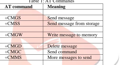
To send SMS messages, a valid SIM card is placed into a GSM modem, which is then connected to the microcontroller by RS232 cable. After connecting a GSM modem to a microcontroller, it can be controlled by sending instructions called AT commands to it. AT commands are used to control MODEMs. AT is the abbreviation for Attention. These commands come from Hayes commands that were used by the Hayes smart modems. The Hayes commands started with AT to indicate the attention from the MODEM. The dial up and wireless MODEMs (devices that involve machine to machine communication) need AT commands to interact with a computer. GSM modems support a common set of standard AT commands. In addition to this common set of standard AT commands, GSM modem supports an extended set of AT commands which is used to control the sending and receiving of SMS messages. The Table1 lists the AT commands that are related to the writing and sending of SMS messages.
w.ijera.com
Table 1: AT Commands
AT command Meaning
+CMGS Send message
+CMSS Send message from storage
+CMGW Write message to memory
+CMGD Delete message
+CMGC Send command
+CMMS More messages to send
One way to send AT commands to a GSM modem is to use a program which sends the characters typed to the GSM modem. It then displays the response which it receives from GSM modem on the screen
2.3. GSM INTERFACING WITH LPC1768
The transmission signal of serial port of microcontroller is connected to T1 IN pin of MAX232 IC. MAX232 IC chips are commonly referred as line drivers, which usually converts RS232 signal (DB9 connector) into TTL voltage levels. T1 OUT pin of MAX232 is connected to RXD pin of GSM modem. Similarly, the TXD pin of GSM modem is connected to RXD (P0.9) pin of LPC1768 through R1 pins of MAX232 IC.
Figure 1: GSM Interfacing with LPC1768
2.4 LCD DISPLAY
The display used here is 16x 2 LCD (Liquid Crystal Display)means 16 characters per line by 2 lines. The standard is referred to as HD44780U, which refers to the controller chip which receives data from an external source (in this case, the LPC1768 microcontroller) and communicates directly with the LCD. The standard LCD requires 3 control lines as well as either 4 or 8 I/O lines for the data bus. Here 4-bit mode of LCD is used with 4-bit data bus.
As shown in Fig. 2,Pin 1 and 2 are the power supply lines, Vss and Vdd. The Vdd pin should be connected to positive supply and Vss to 0V supply or ground. LCD module data sheets specify a 5V DC supply, 6V and 4-5V supplies also work well, and even 3V is sufficient for some modules. Pin 3 is a control pin. Vee, used to alter the contrast of the display. Ideally, this pin should be connected to a variable voltage supply.
Pin 4 is the (RS) register select line. When this line is low, data bytes transferred to the display are treated as commands and data bytes read from the display indicates its status. By setting the RS line high, character data can be transferred to and from the
T1 IN
R1 OUT
MAX 232 T1 OUT R1 IN P0.8 P0.9 LPC 1768
RX TX
IJEDR1502018
International Journal of Engineering Development and Research (www.ijedr.org)91
module. Pin 5 is read/write line. This line is pulled low in order to write commands or character data to the module, or pulled high to read character data or status information from its registers. Pin 6 is the enable line. This input is used to initiate the actual transfer of commands or character data between the module and the data lines. When writing to the display, data is transferred only on high to low transition of this signal. Pin 7 to 14 are data bus lines (D0 to D7).data can be transferred to and from the display either as a single 8 bit byte or two 4 bit nibbles. The other two pins LED+ and LED- is used for back light of the LCD.Figure 2: LCD module Pin Details
2.5 USB HOST CONTROLLER
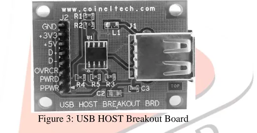
The USB Host Breakout Board is a perfect solution to test USB host feature on USB Host Based Microcontroller Breakout Boards. The USB Host Breakout Board contains all of the digital logic circuitry necessary to implement a full-speed USB host controller. This board can be used to interface and control any USB slave devices like thumb drives, digital cameras, Bluetooth dongles, and much more. The USB Host breakout board has power switch and over-current protection. The board uses circuitry which prevents erroneous over current reporting caused by in-rush currents during hot plug events. This is achieved by the use of LM3526 IC.
Figure 3: USB HOST Breakout Board
The LM3526 provides Universal Serial Bus standard power switch and over current protection for all host port applications. The dual port device is ideal for Notebook and desktop PC's that supply power to more than one port. The dual stage thermal protection circuit in the LM3526 provides individual protection to each switch and the entire device. In a short-circuit/over-current event, the switch dissipating excessive heat is turned, allowing the second switch to continue to function. The LM3526 accepts input voltage between 2.7V and 5.5V.
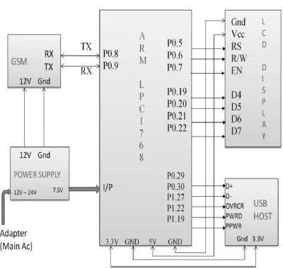
The USB Host Controller Interfacing is as shown in Fig.4. The Port0[29] and Port0[30] pins of LPC1768 are connected to D+ and D- of USB Host Controller. The USB D+ and D- are bidirectional lines. The Port1[27], Port1[22] and Port1[19] of LPC1768 is connected to OVRCR, PWRD and PPWR pins of the USB Host Controller respectively. The OVRCR is an
Over Current Status bit and sets‟1‟ bit when the status of current gets over flow. The PWRD pin indicates the Power Status of the USB Host. The PPWR is a Port Power pin used to indicate the power enable signal of the USB host.
2.6 HARDWARE DESIGN
IJEDR1502018
International Journal of Engineering Development and Research (www.ijedr.org)92
Figure 4: Hardware DesignIII. SOFTWARE DESIGN
3.1 KEIL μVISION
The μVision IDE from Keil, combines project management, make facilities, source code editing, program debugging, and complete simulation in one powerful environment. μVision helps to get programs working faster than ever while providing an easy-to-use development platform. The editor and debugger are integrated into a single application and provide a seamless embedded project development environment.
The μVision 4 IDE is Windows-based softwaredevelopment platforms that combines a robust editor, project manager, and make facility. μVision 4 integrates all tools including the C compiler, macro assembler, linker/locator, and HEX file generator.
The steps followed while using KeilμVision is explained below:
Open Keil IDE installed previously on the personal computer. Creating a New Project, choose the target device “LPC1768”. Add the main source file to the project by Right clicking on Source Group1visible on the left side of the image. Now compile the code using
“Translate” & “Build” icons present on left top of the page. By default Keil compiler do not generate Intel hex file on source compilation. Some need to configure it to produce Hex file as output. By selecting theTarget1 from Project> options for Target „Target1‟ Options for Target ‟Target1‟ window appears. Select “Create Hex File” option in the window. Now Hex File is created and the same is displayed at the bottom of the window. This Hex File can be dumped onto the IC.
3.2 H FLASHER
JTAG/FLASHER is an ARM toolkit designed by the JTAG team. The toolkit includes JTAG Server, Flasher and H-JTAG USB emulator, which support both the debugging and flash programming for different ARM platforms. H-FLASHER has become one of the most popular debugging and programming tools for ARM processors and is widely used in research, development and production. It has been proven by large number of users around the world. H-JTAG is a powerful and reliable toolkit that we can rely on.
H-FlasherFeatures
1. Support on Chip Flash, Nor Flash, SPI Flash and Nand Flash. 2. Support auto flash download during debugging.
3. Support flexible initialization of target.
4. Support automatic verification during programming. 5. Support plain binary format and Intel hex format. 6. Support the save and load of project file.
The steps followed while using H Flasher is explained below.
Double click on H Flasher tool. A Dialogue box appears and then selects „Flash selection‟. Then click on „NXP vendor‟. Click on „Program Selection‟ and select LPC1768 as LPC1768 IC is used here. Now click on “Configuration” and type the appropriate frequency of Microcontroller. Then, select
IJEDR1502018
International Journal of Engineering Development and Research (www.ijedr.org)93
IV. PROPOSED ARCHITECTURE OPERATION
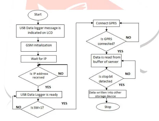
The Microcontroller at the transmitting end reads the data which is stored in the first storage device and sends to the server through GSM/GPRS module. The server starts to communicate with another GSM/GPRS module and sends the data to the second USB storage device at the receiver end. Thus data between two USB storage devices present at different areas is transmitted wirelessly. Display device used here is LCD of 16X2 characters per line for displaying the working conditions of the system [2].
Transmitter Section:
Figure 5: Flowchart of Transmitter Section
Operational frame work of this paper can be divided into two major parts which is shown in Fig. 3 and Fig. 4. Fig .3 shows the flowchart of transmitter section and Fig. 4 shows the flowchart of Receiver section.
Receiver section:
Figure 6: Flowchart of Receiver Section
V. RESULTS AND DISCUSSION
IJEDR1502018
International Journal of Engineering Development and Research (www.ijedr.org)94
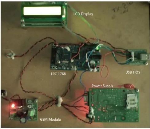
Figure 7: Transmitter kitAt the transmitter end, list of messages are displayed on LCD.
i) LCD displaying the message “USB DATA LOGER" when the device is turned ON.
ii) LCD displaying the message” GSM INT” during initialization of GSM module.
iii) LCD displaying the message “WAITING FOR IP” indicates the device is waiting for the IP address of the server to activate the device.
iv) LCD displaying the IP address and the authorized user phone number as soon as the IP address is received from the user phone.
v) LCD displaying the message “GPRS CONNECTING” as soon as the device receives the IP address from the user cell phone.
vi) LCD displaying the message ”GPRS CONNECTED” as soon as the GPRS activated GSM gains access to the server.
vii) LCD displaying the message ”USB DATA LOGGER READY” indicating that the device is ready to receive the contents and write to the USB storage device connected to it.
IJEDR1502018
International Journal of Engineering Development and Research (www.ijedr.org)95
ix) LCD displaying a message indicating the user that the data has been received by the client/receiver deviceAs soon as the data is received by the server, a dialogue box appears with the following messages as shown below.
At the Receiver end, same procedure is followed frm step i to step ix.LCD displays a message “WRITE COMPLETED” indicates that data is received and written into the second storage device.
When the receiver receives the data from the server, the following messages are displayed in dialogue box at server side.
VI. CONCLUSION
In this paper a prototype for the purpose of remote data acquisition and transmission system using serial communication techniques is discussed. The algorithm for this work is designed for the transmission of Text or doc files only. Necessary changes can be made in the algorithm and can be implemented for transmission and reception of multimedia files. Since here ARM processor is used, the algorithm is simpler. The ARM processor consumes very less power (3.3volts) compared to Microcontroller. Using this prototype, a portable device can be developed which will have the size of a USB storage device and can be carried by the user. Device initialization using IP (internet protocol) address makes it more secure. Using this system, one can transmit data for long distance and simplifying the programmability to make the ARM architecture an option for even complex applications [5].
VII. ACKNOWLEDGMENT
The authors thank the authorities of Sinhgad Institute of Technology for their encouragements.
REFERENCES
[1] Anuj Kumar, I. P. Singh, and S. K. Sud “Design and Development of Multi-Channel Data Logger for Built Environment “, Proceedings of International Multi-Conference of Engineers and Computer scientists 2010 Vol II ,IMECS 2010 ,Hong Kong,PP:993-998
IJEDR1502018
International Journal of Engineering Development and Research (www.ijedr.org)96
[3] O'Brien K, Salyers D.C, Striegel A.D, Poellabauer C ”Power and performance characteristics of USB flashdrives, World of Wireless, Mobile and Multimedia Networks”11th IEEEInternational Symposium.June-2008 and also published in International Journal of Advanced Computer Science and Applications.
[4] Vijay. K. Garg, “Principles and Applications of GSM”, Pearson Education Publisher, First Edition, 1999.
[5] Joseph Yiu, “The Definitive Guide to the ARM CORTEX – M3”, 2nd Edition, Newnes Publisher, 12th January 2010 [6] ShyamSadasivan, “ An Introduction to the ARM CORTEX – M3 Processor”, October 2006
[7] Helms, J., Neale, D.C., Isenhour, P.L. and Carroll, J.M. (2000). Data Logging: Higher-Level Capturing and Multi-Level Abstracting of User Activities. Proceedings of the 40th annual meeting of the Human Factors and Ergonomics Society.PP:303-306
[8] Sifeng Zhang, Keli Zhang, Ping Cao, Yanfang Wang. “Design and Realization of Remote Synchronous Data Transmission System Based on Distributed Architecture of Serial Concurrent Bus”. IEEE proceedings of the 9th International Conference on Electronic Measurement & Instruments. Beijing, China, Aug.2009, Volume 3 PP: 358-362 [9] Good M. The use of logged data in the design of a new text editor. Proceeding of ACM CHI'85 Conference on Human
Factors in Computing Systems1985. New York: Association of Computing Machinery PP: 93-97
[10] Remple, T. B. , Qualcomm, San Diego, CA, USA , June 2003 "USB on-the-go interface for portable devices", Consumer Electronics, IEEE International Conference, ICCE. 2003.