Multi-Input Transformer less Grid-Tied Invertors
with Effective Control Scheme
Narayan Nayak K*
;
Mr. T. Ravichandra**
&
Ranapanga Saidulu***
*M. Tech Student Department of EEE AVN Institute of engg & tech
**Assistant professor Department of EEE AVN Institute of engg & tech
***Associate professorDepartment of EEE AVN Institute of engg & tech
Abstract:
Three-phase transformer less inverter is widely used in low-power photovoltaic (PV) grid-connected systems due to its small size, high efficiency and low cost. When no transformer is used in a grid connected photovoltaic (PV) system, a galvanic connection between the grid and PV array exists. In these conditions, dangerous leakage currents (common-mode currents) can appear through the stray capacitance between the PV array and the ground. The former, in order to create a galvanic isolation between the input and the output include a transformer (mandatory in some countries) that limits the whole system performances in terms of efficiency, weight, size and cost. On the contrary, transformerless inverters do not present any isolation and are characterized by little size, lower cost and higher efficiency (more than 2% higher). Nevertheless, the lack of transformers leads to leakage currents that can be harmful to the human body, as well as for the whole conversion system integrity. In order to minimize the ground leakage current and improve the efficiency of the converter system, transformerless PV inverters utilizing unipolar PWM control. In this project it presents a high-reliability single-phase transformerless grid-connected inverter that operate super junction MOSFETs to accomplish high efficiency for photovoltaic applications. In this paper proposed converter tested for the three phase system and it is analyzed.kept constant at midpoint of dc input voltage, results low leakage current. Finally, to validate the
proposed topology, a 1 kW laboratory prototype is built and tested. The experimental results show that the proposed topology can inject reactive power into the utility grid without any additional current distortion and leakage current. The maximum efficiency and European efficiency of the proposed topology are measured and found to be 98.54% and 98.29%, respectively recently, the photovoltaic power generation system has been focused as one of the most significant energy sources due to the rising concern about global warming, and the increase of electrical power consumption. In addition, the PV module has no moving parts, which have made it very robust, long lifetime and low maintenance device. Though the PV module is still expensive, but due to the large-scale manufacturing it has become increasingly cheaper in the last few years. It has been reported that the milestone of 100GW installed PV power all over the world was achieved at the end of 2012 and increased to 140GW at the end of 2013, and the majority were grid connected. Therefore, a prediction has been made that the future grid tied PV system will play an important role in the regulation of the conventional power system.
from the topology presented to overcome the low reverse-recovery issues of MOSFETs body-diode when injects reactive power into the utility grid. Therefore, the proposed topology can be implemented with MOSFET switches without reliability and efficiency penalty. The proposed topology can also employ unipolar-SPWM with three-level output voltage.
Index Terms—Common mode, converter, high efficiency, leak-age current, reactive power, transformerless.
INTRODUCTION
In recent past years the photovoltaic (PV) systems have been received unprecedented concentration due to the raise of concerns about adverse effects of extensive use of fossil fuels on the environment and energy utilization with security in grid-connected PV systems that are still outnumbered by the power generation schemes which are based on oil or natural gas or coal or nuclear or hydro or wind or any combination of these [1] PV systems capacity is majorly based on the order of tens of megawatts that have been installed and interfaced at the grid level in the primary distribution where the PV system installation at the secondary distribution level are dominated by rooftop units with distinct capacities on the order of a few kilowatts with no significant impact on the existing power systems. An attractive feature of PV systems is that they produce electric power without harming the environment, by directly transforming a free unlimited source of energy, solar radiation, into electricity. This fact along with the continuing decrease in PV arrays cost and the increase in their efficiency has resulted in the use of PV generation systems. In the past, PV sources were commonly used in isolated and stand-alone applications. Nowadays, the trend is to connect the PV systems to the public grid, selling the generated power with advantageous price ratings fixed by governmental policies. High frequency common-mode (CM) voltages
must be avoided for a transformerless PV gridconnected inverter because it will lead to a largecharge/discharge current partially flowing through the inverter to the ground. This CM ground current will cause an increase in the current harmonics, higher losses, safety problems, and electromagnetic interference (EMI) issues For a grid-connected PV system, energy yield and payback time are greatly dependant on the inverter’s reliability and efficiency, which are regarded as two of the most significant characteristics for PV inverters.
inverter are avoided in the H6 inverter topology improving efficiency; however, there are higher conduction losses due to the three series-connected switches in the current path during active phases. The shootthrough issues due to three active switches series connected to the dc-bus still remain in the H6 topology. Another disadvantage to the H6 inverter is that when the inverter output voltage and current has a phase shift the MOSFET body diodes may be activated. This can cause body diode reverse-recovery issues and decrease the reliability of the system.
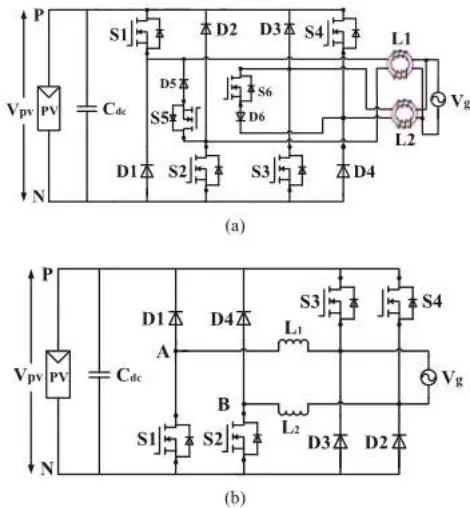
Fig1. Single-phase transformerless PV inverters using super junction MOSFETs: (a) H5, (b) H6, and (c) dualparalleled-buck inverters
requirements at every PWM switching commutation instant as well as at grid zero-crossing instants, 3) minimized CM leakage current because there are two additional ac-side switches that decouple the PV array from the grid during the freewheeling phases, and 4) all the active switches of the proposed converter can reliably employ super junction MOSFETs since it never has the chance to induce MOSFET body diode reverse recovery. As a result of the low conduction and switching losses of the superjunction MOSFETs, the proposed converter can be designed to operate at higher switching frequencies while maintaining high system efficiency. Higher switching frequencies reduce the ac-current ripple and the size of passive components.
Wind Energy and Wind Power
Wind is a form of solar energy. Winds are caused by the uneven heating of the atmosphere by the sun, the irregularities of the earth's surface, and rotation of the earth. Wind flow patterns are modified by the earth's terrain, bodies of water, and vegetative cover. This wind flow, or motion energy, when "harvested" by modern wind turbines, can be used to generate electricity.
How Wind Power Is Generated
The terms "wind energy" or "wind power" describe the process by which the wind is used to generate mechanical power or electricity. Wind turbines convert the kinetic energy in the wind into mechanical power. This mechanical power can be used for specific tasks (such as grinding grain or pumping water) or a generator can convert this mechanical power into electricity to power homes, businesses, schools, and the like.
Fig 2.Wind turbines
II.
PROPOSED TOPOLOGY AND
OPERATING PRINCIPLE
A. Structure of the Proposed Topology
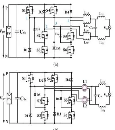
Fig. 4 shows the proposed transformerless inverter topolo-gies consisting of six MOSFET switches (S1-S6) and six diodes (D1-D6). L1A,
L1B, L2A, L2B, L1g, L2g and Co make up the LCL
type filter connected to the grid. VPV and Cdc
B. Operating Principle of the Proposed Topology
The switching pattern of the proposed topology is shown in Fig. 5, where G1, G2, G3, G4, G5, and G6 represent the gate drive signals of the switches S1, S2, S3, S4, S5, and S6, respec-tively. The operation principle of the proposed topology within a grid period is divided into four regions as shown in Fig. 5. Due to the symmetry of the operation of the positive and neg-ative half cycle of grid current, here only positive half cycle explanation is given. However, the circuit diagram for negative half cycle operation is depicted in Fig. 6.
Region I: In this region, both the grid current and voltage are positive. During the period within this region, S2 is always on,
Fig. 2. Some existing transformerless topologies for grid-tied PV system using MOSFETs as main power switches
Fig. 3. High efficiency transformerless topology
while S1 & S3 synchronously and S5 complementary commu-tate with switching frequency. There are always two states that generate the output voltage of +VPV and 0.
State 1(t0:t1): At t = t0, the switches S1 & S3 are turned-on and the inductor current increases through grid as shown in Fig. 6(a). In this state, the voltages V1N and V2N can be defined as: V1N
= +VP V and V2N = 0, thus the inverter output
voltage
V12 = (V1N − V2N ) = +VP V .
State 2(t1:t2): When the switches S1 and S3 are turned-off, the inductor current freewheels through S2 and D5. In this state, V1N falls and
V2N rises until their values are equal. Therefore,
the voltages V1N and V2N becomes: V1N = VP V
/2 and V2N = VP V /2 and the inverter output
voltage V12 = 0.
Fig. 4. (a) Circuit structure of the proposed transformerless topology for grid-tied PV system (b) circuit structure with coupled inductor.
Fig. 5. Switching pattern of the proposed topology with reactive power flow.
complementary commutate with switching frequency. There are also two states that generate the output voltage of −VPV and 0.
State 3(t3:t4): In this state, the switches S4 and S6 are turned-on and the filter inductors are demagnetized. Since the inverter output voltage is negative and the current remains
Fig. 6. The operating principle of the proposed topology: (a) state 1 (b) state 2
(c) state 3 (d) state 4 (e) state 5 (f) state 6.
positive; therefore, the inductor current is forced to freewheel through the diode D1 and D2, and decreases rapidly for enduring the reverse voltage as shown in Fig. 6(c). The voltages V1N and V2N can be defined as: V1N =0and V2N =+VPV, thus the inverter output voltage V12 =(V1N −V2N)=−VPV. State 4(t4:t5): At t = t4, the switches S4 and S6 are turnedoff and S2 is turned-on. Therefore, the inductor current flows through S2 and D5 like as state 2 (Fig. 6(b) can be referred as equivalent circuit). This state is called as energy storage mode. ThevoltagesV1N andV2N couldbe:V1N = VPV/2andV2N = VPV/2, and thus the inverter output voltage, V12 =0
III. HIGH FREQUENCY CM MODEL
OF THE PROPOSED TOPOLOGY FOR
LEAKAGE
CURRENT ANALYSIS
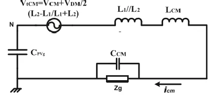
the grid, a CM resonant circuit can be created. An alternating CM voltage that dependsonthetopologystructureandcontrolschem e,canelectrify the resonant circuit and may lead to higher ground leakage current [6], [16], [22]. In order to analyze the CM characteristics, an equivalent circuit of the proposed topology as shown in Fig. 7 can be drawn, where V1N,V2N,V3N and V4N are the controlled voltage source connected to the negative terminal N, LCM and CCM are the CM inductor and capacitor, CPVg is the parasitic capacitance, and Zg is the grid impedance. During the positive half-cycle, the switches S4 and S6 are always off. As a result, the controlled voltage sources V3N and V4N are zero and can be removed. According to the definition of common-mode and differential-mode voltage:
Solving (1) and (2), V1N and V2N can be expressed as follows:
Fig. 9. Simplified single loop CM model
In order to illustrate the CM model at switching frequency, equation (3) and (4) could be replaced for the bridge-leg in Fig. 7. The grid is a low frequency (50–60 Hz) voltage source; thus the impact of grid on the leakage current can be neglected [23]. The DM capacitor Co can also be removed since it has no effect on the leakage current. Consequently, the simplified high frequency CM model of the proposed topology for positive half-cycle could be drawn as Fig. 8. Finally, the simplified single loop CM model of the proposed topology for positive half cycle is derived in Fig. 9. From Fig. 9, the following equation of the total CM voltage can easily be derived as:
where VtCM represent total CM voltage, and L1 = L1A + L1g and L2 = L1B + L2g. In the proposed inverter if L1A = L1B and L1g = L2g for a well-designed circuit with symmetrically structured magnetics [16], equation (5) can be rewritten as
According to the operation principle of the proposed topology presented in section II (B), the total CM voltages can be calculated for each state of positive half cycle operation as follows:
It is clear from equations (7)-(10) that the total CM voltage for the proposed topology during positive half cycle operation is kept constant at VPV/2. Likewise, the total CM voltage for the negative half cycle operation can be calculated and found to be constant at VPV/2 due to the symmetry of operation for the positive and negative half cycle of grid current. The only difference is the activation of different power devices. Therefore, it can be concluded that the total CM voltage during the whole grid cycle is kept constant, reducing ground leakage current.
IV.
PROPOSED
TOPOLOGY
CONTROL
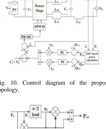
Thecontrolsystemfortheproposedtopologyisillust ratedin Fig. 10, which contains an orthogonal signal generator (OSG) unit to calculate active and reactive power, two proportional integral (PI) controllers, a grid current controller and a SPWM generation block. Based on the OSG system, the active power P and reactive power Q for the proposed topology can be calculated by using the following equation which is shown in Fig. 11 [4], [24]:
Pcal =1 /2[vgαigα + vgβigβ] (11) Qcal =1
/2[vgβigα −vgαigβ] (12)
wherevgα,vgβ,igα,andigβ representstheαandβ
components of grid voltage and current. Based on equation(11)and(12),the current in αβ-reference frame can be derived as follows: igα =2(Pcal ∗vgα + Qcal ∗vgβ)/_v2gα + v2gβ_ (13) igβ =2(Pcal ∗vgβ + Qcal ∗vgα)/_v2gα + v2gβ_ (14) According to the single phase P-Q theory, the grid-in current reference can be generated by regulating the averaged active and reactive power [25], [26]. Since the active and reactive power are constant in steady state, so to control them two PI
Fig. 10. Control diagram of the proposed topology.
Fig. 11. OSG based power calculation.
where Pref and Qref are the power references, Gp(s) and Gq(s) are the transfer function of PI based controller that can be defined as follows:
where Kpp,Kpi,Kqp,and Kqi
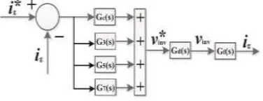
aretheproportionalandintegral gain for the active and reactive power. In order to control the grid current, several existing control methodssuchasconventionalPIcontroller,repetiti vecontroller (RC), proportional resonant (PR) controller, and deadbeat (DB) controller can be adopted due to the capability of tracking reference signal without steady state error [27], [28]. Since the PR controller has better performance of tracking the reference signal if compared to the normal PI and RC controller, it is selected to control the output current of the proposed topology. The block diagram of the PR controller with harmonic current compensator is shown in Fig. 12, where Gc(s), Gh(s), and Gd(s) are the transfer function of fundamental current controller, harmonic compensator, and inverter respectively. The transfer functions are given below [27], [29]:
Fig. 12. Block diagram of PR controller with harmonic compensator.
TABLE I SPECIFICATION OF THE
PROTOTYPE
whereKpi andKii
aretheproportionalandresonantgain,ωf is the fundamental frequency, Kih is the resonant gain at the nthorder harmonic, h is the harmonic order, and Ts is the sampling period.
V. SIMULATION RESULTS
is only 10 mA which is far lower than the limitation requirement of the German standard [30]. Figs. 15 and 16 show the dynamic results under the changes of only Pref, and both Pref and Qref. It is clear that the grid current is changed according to the step load changes, and
Fig.13 Circuit diagram
Fig.14 Inverter 3-level output voltage
Fig.14 Load and grid voltage
the active and reactive power controller track the reference power within four cycle of operation. As seen, the grid current and voltage has very low distortion and the leakage flows through the whole system is very less. Therefore, it can be concluded that the fast and effective response of the load changes are achieved which validate the robustness of the proposed topology with the presented control scheme.
VII. CONCLUSION
This paper explains a new high efficiency transformerless topology for grid-tied PV system is presented. The main advantages of the proposed topology can be summarized as:
o The inherent circuit configuration of the proposed topology does not lead itself to the reverse recovery issues which allow utilizing MOSFET switches even though when inject reactive power. Therefore, without compromising the overall efficiency, proposed topology can inject reactive power into the utility grid.
TheCMvoltageiskeptconstantatthemid-pointofdcbus voltage; as a result, low leakage current flows through the system which is lower than the H6-type topology.
PWMdeadtimeisnotrequiredfortheproposedt opology that reduces the THD at the output. Finally, to demonstrate the feasibility and effectiveness of the proposed topology, a 1 kW laboratory prototype is built and tested with both real and reactive power injection. The experimental results verified the above mentioned advantages. It has shown that the proposed topology presents almost the same characteristics for both real and reactive power injection, which are very suitable for grid-tied PV system. Therefore, it can be concludedthattheproposedinverterisanattract ivesolutionfor grid-tied PV system.
REFERENCES
[1]I. Patrao, E. Figueres, F. González-Espín, and G. Garcerá, ―Transformerless topologies for grid-connected single-phase photo-voltaic inverters,‖ Renew. Sustain. Energy Rev., vol. 15, pp. 3423–3431, 2011.
[2]M. Islam, S. Mekhilef, and M. Hasan, ―Single phase transformerless inverter topologies for grid-tied photovoltaic system: A review,‖ Renew. Sustain. Energy Rev., vol. 45, pp. 69–86, 2015.
[3]I. PVPS, ―Trends in photovoltaic applications. Survey report of selected IEA countries between 1992 and 2013,‖ International Energy Agency, St. Ursen, Switzerland, Report IEA-PVPS T1–25, 2014.
[4]Y. Yang and F. Blaabjerg, ―Low-voltage ride-through capability of a single-stage single-phase photovoltaic system connected to the low-voltage grid,‖ Int. J. Photoenergy, vol. 2013, pp. 1–9, 2013.
[5]S. B. Kjaer, J. K. Pedersen, and F. Blaabjerg, ―A review of single-phase grid-connected inverters for photovoltaic modules,‖ IEEE Trans. Ind. Appl., vol. 41, no. 5, pp. 1292–1306, Sep./Oct. 2005.
[6]X. Huafeng and X. Shaojun, ―Leakage current analytical model and application in single-phase transformerless photovoltaic grid-connected inverter,‖ IEEE Trans. Electromagn. Compat., vol. 52, no. 4, pp. 902–913, Nov. 2010.
[7]T. Kerekes, R. Teodorescu, P. Rodriguez, G. Vazquez, and E. Aldabas, ―A new high-efficiency single-phase transformerless PV inverter topol-ogy,‖ IEEE Trans. Ind. Electron., vol. 58, no. 1, pp. 184–191, Jan. 2011.
[8]Y. Bo, L. Wuhua, G. Yunjie, C. Wenfeng,
and H. Xiangning, ―Improved
transformerless inverter with common-mode leakage current elimination for a photovoltaic grid-connected power system,‖ IEEE Trans. Power Electron., vol. 27, no. 2, pp. 752–762, Feb. 2012.
[9]M. Islam and S. Mekhilef, ―H6-type transformerless single-phase inverter for grid-tied photovoltaic system,‖ IET Power Electron., vol. 8, pp. 636– 644, 2015. [10] O. Lopez et al., ―Eliminating ground
current in a transformerless pho-tovoltaic application,‖ IEEE Trans. Energy Convers., vol. 25, no. 1,
pp.140–147, Mar. 2010.
[11] Z. Li, S. Kai, F. Lanlan, W. Hongfei, and X. Yan, ―A family of neutral point clamped full-bridge topologies for transformerless photo-voltaic grid-tied inverters,‖ IEEE Trans. Power Electron., vol. 28, no. 2,
pp.730–739, Feb. 2013.
[12] T. F. Wu, C. L. Kuo, K. H. Sun, and H. C. Hsieh, ―Combined unipolar and bipolar PWM for current distortion improvement during power com-pensation,‖ IEEE Trans. Power Electron., vol. 29, no. 4, pp. 1702– 1709, Apr. 2014.
[13] W. Yu, J.-S. Lai, H. Qian, and C. Hutchens, ―High-efficiency MOSFET inverter with H6-type configuration for photovoltaic nonisolated AC-module applications,‖ IEEE Trans. Power Electron., vol. 26, no. 4,
[14] X. Huafeng, X. Shaojun, C. Yang, and H. Ruhai, ―An optimized transformerless photovoltaic grid-connected inverter,‖ IEEE Trans. Ind. Electron., vol. 58, no. 5, pp. 1887–1895, May 2011.
[15] R. Gonzalez, J. Lopez, P. Sanchis, and L. Marroyo, ―Transformerless inverter for single-phase photovoltaic systems,‖ IEEE Trans. Power Electron., vol. 22, no. 2, pp. 693–697, Mar. 2007.
[16] G. Bin, J. Dominic, L. Jih-Sheng, C. Chien-Liang, T. LaBella, and C. Baifeng, ―High reliability and efficiency single-phase transformerless inverter for grid-connected photovoltaic systems,‖ IEEE Trans. Power Electron., vol. 28, no. 5, pp. 2235–2245, May 2013.
[17] S. V. Araujo, P. Zacharias, and R. Mallwitz, ―Highly efficient single-phase transformerless inverters for grid-connected photovoltaic systems,‖ IEEE Trans. Ind. Electron., vol. 57, no. 9, pp. 3118–3128, Sep. 2010.
[18] D. Schmidt, D. Siedle, and J. Ketterer, ―Inverter for transforming a DC voltage into an AC current or an AC voltage,‖ EP Patent 1, 369, 985, 2009.
[19] J. Baojian, W. Jianhua, and Z. Jianfeng,
―High-efficiency single-phase
transformerless PV H6 inverter with hybrid modulation method,‖ IEEE Trans. Ind. Electron., vol. 60, no. 5, pp. 2104–2115, May 2013.
[20] M. Islam and S. Mekhilef, ―High efficiency transformerless MOSFET inverter for grid-tied photovoltaic system,‖ in Proc. 29th Annu. IEEE Appl. Power Electron. Conf. Expo. (APEC), 2014, pp. 3356–3361. [21] M. Victor, F. Greizer, S. Bremicker, and
U. Hübler, ―Method of convert-ing a direct current voltage from a source of direct current voltage, more specifically from a photovoltaic source of direct current voltage, into a alternating current voltage,‖ U.S. Patents 7 411 802 B2, 2008.
[22] M. Islam and S. Mekhilef, ―An improved transformerless grid connected photovoltaic inverter with reduced leakage
current,‖ Energy Convers. Manage., vol. 88, pp. 854–862, 2014.
[23] E. Gubía, P. Sanchis, A. Ursúa, J. López, and L. Marroyo, ―Ground currents in single-phase transformerless photovoltaic systems,‖ Progr. Photovoltaics Res. Appl., vol. 15, pp. 629–650, 2007.
[24] S. Dasgupta, S. K. Sahoo, and S. K. Panda, ―Single-phase inverter control techniques for interfacing renewable energy sources with microgrid-part I: Parallel-connected inverter topology with active and reactive power flow control along with grid current shaping,‖ IEEE Trans. Power Electron., vol. 26, no. 3, pp. 717–731, Mar. 2011.
[25] Y. Yongheng, F. Blaabjerg, and W. Huai, ―Low-voltage ride-through of single-phase transformerless photovoltaic inverters,‖ IEEE Trans. Ind. Appl., vol. 50, no. 3, pp. 1942–1952, May/Jun. 2014.
Authors Details:
NARAYAN NAYAK K
RANAPANGA SAIDULU
He received B.Tech. degree in Electrical Engineering from JNT University Hyderabad, India. And M.Tech from JNTU Hyderabad, India. He is currently an Assistant Professor in Electrical and Electronics Engineering department, AVN Institute of Engineering and Technology, JNTU Hyderabad, India. His area of interests include power electronics converters for Renewable Energy Systems, Grid connected power converters and Power Quality Issues.
Mr. T.Ravichandra