LT3470
1
3470fdTypical applicaTion
FeaTures
applicaTions
DescripTion
Micropower Buck Regulator
with Integrated Boost and
Catch Diodes
The LT®3470 is a micropower step-down DC/DC con-verter that integrates a 300mA power switch, catch diode and boost diode into low profile 3mm × 2mm DD and ThinSOT™ packages. The LT3470 combines Burst Mode and continuous operation to allow the use of tiny induc-tor and capaciinduc-tors while providing a low ripple output to loads of up to 200mA.
With its wide input range of 4V to 40V, the LT3470 can regulate a wide variety of power sources, from 2-cell Li-Ion batteries to unregulated wall transformers and lead-acid batteries. Quiescent current in regulation is just 26µA in a typical application while a zero current shutdown mode disconnects the load from the input source, simplifying power management in battery-powered systems. Fast current limiting and hysteretic control protects the LT3470 and external components against shorted outputs, even at 40V input.
L, LT, LTC, LTM, Linear Technology, the Linear logo and Burst Mode are registered trademarks
and ThinSOT is a trademark of Linear Technology Corporation. All other trademarks are the property of their respective owners.
Efficiency and Power Loss vs Load Current
n Low Quiescent Current: 26µA at 12V
IN to 3.3VOUT
n Integrated Boost and Catch Diodes
n Input Range: 4V to 40V n Low Output Ripple: <10mV n <1µA in Shutdown Mode n Output Voltage: 1.25V to 16V n 200mA Output Current n Hysteretic Mode Control
– Low Ripple Burst Mode® Operation at Light Loads – Continuous Operation at Higher Loads
n Solution Size as Small as 50mm2
n Low Profile (0.75mm) 3mm × 2mm Thermally Enhanced 8-Lead DD and 1mm ThinSOT Packages
n Automotive Battery Regulation n Power for Portable Products n Distributed Supply Regulation n Industrial Supplies
n Wall Transformer Regulation
LOAD CURRENT (mA) 30 EFFICIENCY (%) POWER LOSS (mW) 40 60 80 90 0.1 10 100 3470 TA02 20 1 70 50 10 1 1000 100 10 0.1 VIN = 12V VIN BOOST LT3470 SW SHDN 0.22µF 22pF 22µF 2.2µF 3470 TA01a VIN 7V TO 40V VOUT 5V 200mA 604k 1% 200k 1% 33µH BIAS FB GND OFF ON
LT3470
2
3470fdabsoluTe MaxiMuM raTings
VIN, SHDN Voltage ... 40V BOOST Pin Voltage ... 47V BOOST Pin Above SW Pin ... 25V FB Voltage ... 5V BIAS Voltage ...25V SW Voltage ...VIN Maximum Junction TemperatureLT3470E, LT3470I ... 125°C LT3470H ... 150°C
(Note 1)
orDer inForMaTion
Operating Temperature Range (Note 2)
LT3470E ...–40°C to 85°C LT3470I ... –40°C to 125°C LT3470H ... –40°C to 150°C Storage Temperature Range ... –65°C to 150°C Lead Temperature (Soldering, 10 sec) ...300°C
TOP VIEW 9 DDB8 PACKAGE 8-LEAD (3mm × 2mm) PLASTIC DFN 5 6 7 8 4 3 2 1 FB BIAS BOOST SW SHDN NC VIN GND θJA = 180°C/W
EXPOSED PAD (PIN 9) IS GROUND (MUST BE SOLDERED TO PCB)
SHDN 1 NC 2 VIN 3 GND 4 8 FB 7 BIAS 6 BOOST 5 SW TOP VIEW TS8 PACKAGE 8-LEAD PLASTIC TSOT-23
θJA = 140°C/W
pin conFiguraTion
LEAD FREE FINISH TAPE AND REEL PART MARKING PACKAGE DESCRIPTION TEMPERATURE RANGE
LT3470EDDB#PBF LT3470EDDB#TRPBF LBPN 8-Lead (3mm × 2mm) Plastic DFN –40°C to 85°C LT3470IDDB#PBF LT3470IDDB#TRPBF LBPP 8-Lead (3mm × 2mm) Plastic DFN –40°C to 125°C LT3470HDDB#PBF LT3470HDDB#TRPBF LCNR 8-Lead (3mm × 2mm) Plastic DFN –40°C to 150°C LT3470ETS8#PBF LT3470ETS8#TRPBF LTBDM 8-Lead Plastic TSOT-23 –40°C to 85°C LT3470ITS8#PBF LT3470ITS8#TRPBF LTBPW 8-Lead Plastic TSOT-23 –40°C to 125°C LT3470HTS8#PBF LT3470HTS8#TRPBF LTCNQ 8-Lead Plastic TSOT-23 –40°C to 150°C
LEAD BASED FINISH TAPE AND REEL PART MARKING PACKAGE DESCRIPTION TEMPERATURE RANGE
LT3470EDDB LT3470EDDB#TR LBPN 8-Lead (3mm × 2mm) Plastic DFN –40°C to 85°C LT3470IDDB LT3470IDDB#TR LBPP 8-Lead (3mm × 2mm) Plastic DFN –40°C to 125°C LT3470HDDB LT3470HDDB#TR LCNR 8-Lead (3mm × 2mm) Plastic DFN –40°C to 150°C LT3470ETS8 LT3470ETS8#TR LTBDM 8-Lead Plastic TSOT-23 –40°C to 85°C LT3470ITS8 LT3470ITS8#TR LTBPW 8-Lead Plastic TSOT-23 –40°C to 125°C LT3470HTS8 LT3470HTS8#TR LTCNQ 8-Lead Plastic TSOT-23 –40°C to 150°C Consult LTC Marketing for parts specified with wider operating temperature ranges.
For more information on lead free part marking, go to: http://www.linear.com/leadfree/
LT3470
3
3470fd
The l denotes the specifications which apply over the full operating
temperature range, otherwise specifications are at TA = 25°C. VIN = 10V, VSHDN = 10V, VBOOST = 15V, VBIAS = 3V unless otherwise specified.
Note 1: Stresses beyond those listed under Absolute Maximum Ratings
may cause permanent damage to the device. Exposure to any Absolute Maximum Rating condition for extended periods may affect device reliability and lifetime.
Note 2: The LT3470E is guaranteed to meet performance specifications
from 0°C to 85°C. Specifications over the –40°C to 85°C operating temperature range are assured by design, characterization and correlation with statistical process controls. The LT3470I specifications
are guaranteed over the –40°C to 125°C temperature range. LT3470H specifications are guaranteed over –40°C to 150°C temperature range.
Note 3: Bias current flows out of the FB pin.
Note 4: This is the minimum voltage across the boost capacitor needed to
guarantee full saturation of the switch.
Note 5: This parameter is assured by design and correlation with statistical
process controls.
elecTrical characTerisTics
PARAMETER CONDITIONS MIN TYP MAX UNITS
Minimum Input Voltage ● 4 V
Quiescent Current from VIN VSHDN = 0.2V
VBIAS = 3V, Not Switching
VBIAS = 0V, Not Switching
● 0.1 10 35 0.5 18 50 µA µA µA Quiescent Current from Bias VSHDN = 0.2V
VBIAS = 3V, Not Switching
VBIAS = 0V, Not Switching
● 0.1 25 0.1 0.5 60 1.5 µA µA µA FB Comparator Trip Voltage VFB Falling ● 1.228 1.250 1.265 V
FB Pin Bias Current (Note 3) VFB = 1V, E- and I-Grade
●
35
35 15080 nA nA
H-Grade ● 35 225 nA
FB Voltage Line Regulation 4V < VIN < 40V 0.0006 0.01 %/V
Minimum Switch Off-Time (Note 5) 500 ns
Switch Leakage Current 0.7 1.5 µA
Switch VCESAT ISW = 100mA (TS8 Package)
ISW = 100mA (DD8 Package)
215
215 300 mV mV
Switch Top Current Limit VFB = 0V 250 325 435 mA
Switch Bottom Current Limit VFB = 0V 225 mA
Catch Schottky Drop ISH = 100mA (TS8 Package)
ISH = 100mA (DD8 Package)
630
630 775 mV mV
Catch Schottky Reverse Leakage VSW = 10V 0.2 2 µA
Boost Schottky Drop ISH = 30mA 650 775 mV
Boost Schottky Reverse Leakage VSW = 10V, VBIAS = 0V 0.2 2 µA
Minimum Boost Voltage (Note 4) ● 1.7 2.2 V
BOOST Pin Current ISW = 100mA 7 12 mA
SHDN Pin Current VSHDN = 2.5V 1 5 µA
SHDN Input Voltage High 2.5 V
LT3470
4
3470fdTypical perForMance characTerisTics
Efficiency, VOUT = 3.3V Efficiency, VOUT = 5V VFB vs Temperature
Top and Bottom Switch Current Limits (VFB = 0V) vs Temperature
VIN Quiescent Current
vs Temperature BIAS Quiescent Current (Bias > 3V) vs Temperature
SHDN Bias Current
vs Temperature FB Bias Current (Vvs Temperature FB = 1V) LOAD CURRENT (mA)
50 EFFICIENCY (%) 70 90 40 60 80 0.1 10 100 3470 G01 30 1 L = TOKO D52LC 47µH TA = 25°C V VIN = 7V IN = 12V VIN = 36V VIN = 24V
LOAD CURRENT (mA) 50 EFFICIENCY (%) 70 90 40 60 80 0.1 10 100 3470 G02 30 1 L = TOKO D52LC 47µH TA = 25°C VIN = 12V VIN = 36V VIN = 24V TEMPERATURE (°C) –50 1.240 VFB (V) 1.245 1.250 1.255 1.260 –25 0 25 50 3470 G03 75 100 125 TEMPERATURE (°C) –50
CURRENT LIMIT (mA)
350 25 3470 G04 200 100 –25 0 50 50 0 400 300 250 150 75 100 125 150 TEMPERATURE (°C) –50 –25 0 VIN CURRENT (µA) 20 50 0 50 75 3470 G05 10 40 30 25 100 125 150 BIAS < 3V BIAS > 3V TEMPERATURE (°C) –50
BIAS CURRENT (µA)
20 25 30 25 75 3470 G06 15 10 –25 0 50 100 125 150 5 0 TEMPERATURE (°C) –50 0 SHDN CURRENT (µA) 1 3 4 5 50 9 3470 G07 2 0 –25 25 75 100 125 150 6 7 8 VSHDN = 36V VSHDN = 2.5V TEMPERATURE (°C) –50 –25 0 FB CURRENT (nA) 20 60 50 0 50 75 3470 G08 10 40 30 25 100 125 150
LT3470
5
3470fd
Typical perForMance characTerisTics
FB Bias Current (VFB = 0V)
vs Temperature vs TemperatureSwitch VCESAT (ISW = 100mA) Boost Diode Vvs TemperatureF (IF = 50mA)
Catch Diode VF (IF = 100mA)
vs Temperature vs TemperatureDiode Leakage (VR = 36V) Switch VCESAT
BOOST Pin Current Catch Diode Forward Voltage TEMPERATURE (°C) –50 FB CURRENT (µA) 80 100 120 25 75 3470 G09 60 40 –25 0 50 100 125 150 20 0 TEMPERATURE (°C) –50 SWITCH V CESAT (mV) 200 250 300 25 75 3470 G10 150 100 –25 0 50 100 125 150 50 0 TEMPERATURE (°C) –50 SCHOTTKY V F (V) 0.7 25 3470 G11 0.4 0.2 –25 0 50 0.1 0 0.8 0.6 0.5 0.3 75 100 125 150 TEMPERATURE (°C) –50 0.4 0.5 0.7 25 75 3470 G12 0.3 0.2 –25 0 50 100 125 150 0.1 0 0.6 SCHOTTKY V F (V) TEMPERATURE (°C) –50 –25 0
SCHOTTKY DIODE LEAKAGE (µA)
30 60 0 50 75 3470 G13 20 15 10 50 40 25 55 5 45 35 25 100 125 150 CATCH BOOST
SWITCH CURRENT (mA) 0 400 500 700 300 3470 G14 300 200 100 200 400 100 0 600 SWITCH V CESAT (mV)
SWITCH CURRENT (mA) 0 8 10 14 300 3470 G15 6 4 100 200 400 2 0 12
BOOST PIN CURRENT (mA)
CATCH DIODE CURRENT (mA) 0 SCHOTTKY V F (V) 0.4 0.6 400 3470 G16 0.2 0 100 200 300 1.0 0.8
LT3470
6
3470fdSHDN (Pin 1/Pin 8): The SHDN pin is used to put the LT3470 in shutdown mode. Tie to ground to shut down the LT3470. Apply 2V or more for normal operation. If the shutdown feature is not used, tie this pin to the VIN pin. NC (Pin 2/Pin 7): This pin can be left floating or connected to VIN.
VIN (Pin 3/Pin 6): The VIN pin supplies current to the LT3470’s internal regulator and to the internal power switch. This pin must be locally bypassed.
GND (Pin 4/Pin 5): Tie the GND pin to a local ground plane below the LT3470 and the circuit components. Return the feedback divider to this pin.
SW (Pin 5/Pin 4): The SW pin is the output of the internal power switch. Connect this pin to the inductor, catch diode and boost capacitor.
BOOST (Pin 6/Pin 3): The BOOST pin is used to provide a drive voltage, which is higher than the input voltage, to the internal bipolar NPN power switch.
BIAS (Pin 7/Pin 2): The BIAS pin connects to the internal boost Schottky diode and to the internal regulator. Tie to VOUT when VOUT > 2V or to VIN otherwise. When VBIAS > 3V the BIAS pin will supply current to the internal regulator. FB (Pin 8/Pin 1): The LT3470 regulates its feedback pin to 1.25V. Connect the feedback resistor divider tap to this pin. Set the output voltage according to VOUT = 1.25V (1 + R1/R2) or R1 = R2 (VOUT/1.25 – 1).
Exposed Pad (DD, Pin 9): Ground. Must be soldered to PCB.
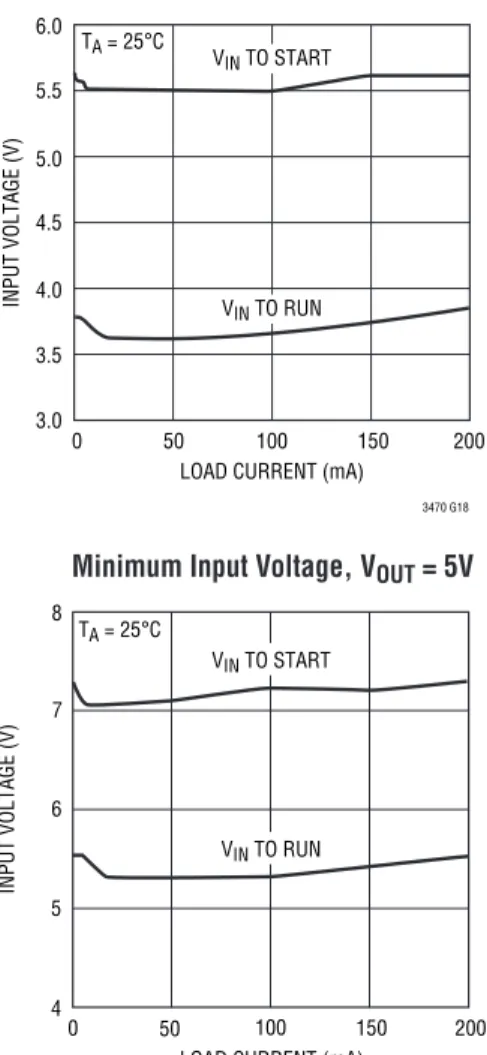
Boost Diode Forward Voltage Minimum Input Voltage, VOUT = 3.3V Minimum Input Voltage, VOUT = 5V
Typical perForMance characTerisTics
BOOST DIODE CURRENT (mA) 0 SCHOTTKY V F (V) 500 600 700 200 3470 G17 400 300 0 50 100 150 100 200 900 800
LOAD CURRENT (mA) 0 3.0 INPUT VOLTAGE (V) 3.5 4.0 4.5 5.0 5.5 6.0 50 100 150 200 3470 G18 TA = 25°C V IN TO START VIN TO RUN
LOAD CURRENT (mA) 0 INPUT VOLTAGE (V) 6 7 200 3470 G19 5 4 50 100 150 8 TA = 25°C VIN TO START VIN TO RUN
LT3470
7
3470fdblock DiagraM
– + – + R Q′ S Q 500ns ONE SHOT VREF 1.25V Burst Mode DETECT SW GND 3470 BD FB R2 R1 SHDN ENABLE VIN VIN NC BIAS BOOST L1 C2 C3 VOUT gm C1LT3470
8
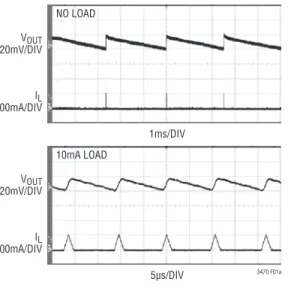
3470fdFigure 1. Operating Waveforms of the LT3470 Converting 12V to 5V Using a 33µH Inductor and 10µF Output Capacitor
The LT3470 uses a hysteretic control scheme in conjunction with Burst Mode operation to provide low output ripple and low quiescent current while using a tiny inductor and capacitors.
Operation can best be understood by studying the Block Diagram. An error amplifier measures the output voltage through an external resistor divider tied to the FB pin. If the FB voltage is higher than VREF, the error amplifier will shut off all the high power circuitry, leaving the LT3470 in its micropower state. As the FB voltage falls, the error amplifier will enable the power section, causing the chip to begin switching, thus delivering charge to the output capacitor. If the load is light the part will alternate between micropower and switching states to keep the output in regulation (See Figure 1a). At higher loads the part will switch continuously while the error amp servos the top and bottom current limits to regulate the FB pin voltage to 1.25V (See Figure 1b).
The switching action is controlled by an RS latch and two current comparators as follows: The switch turns on, and the current through it ramps up until the top current
comparator trips and resets the latch causing the switch to turn off. While the switch is off, the inductor current ramps down through the catch diode. When both the bot-tom current comparator trips and the minimum off-time one-shot expires, the latch turns the switch back on thus completing a full cycle. The hysteretic action of this control scheme results in a switching frequency that depends on inductor value, input and output voltage. Since the switch only turns on when the catch diode current falls below threshold, the part will automatically switch slower to keep inductor current under control during start-up or short-circuit conditions.
The switch driver operates from either the input or from the BOOST pin. An external capacitor and internal diode is used to generate a voltage at the BOOST pin that is higher than the input supply. This allows the driver to fully saturate the internal bipolar NPN power switch for efficient operation.
If the SHDN pin is grounded, all internal circuits are turned off and VIN current reduces to the device leakage current, typically a few nA.
(1a) Burst Mode Operation (1b) Continuous Operation
VOUT 20mV/DIV IL 100mA/DIV 1ms/DIV VOUT 20mV/DIV IL 100mA/DIV 5µs/DIV 3470 F01a NO LOAD 10mA LOAD VOUT 20mV/DIV IL 100mA/DIV 1µs/DIV VOUT 20mV/DIV IL 100mA/DIV 1µs/DIV 3470 F1b 200mA LOAD 150mA LOAD
operaTion
LT3470
9
3470fd
applicaTions inForMaTion
Input Voltage Range
The minimum input voltage required to generate a par-ticular output voltage in an LT3470 application is limited by either its 4V undervoltage lockout or by its maximum duty cycle. The duty cycle is the fraction of time that the internal switch is on and is determined by the input and output voltages:
DC= VOUT+VD VIN– VSW+VD
where VD is the forward voltage drop of the catch diode (~0.6V) and VSW is the voltage drop of the internal switch at maximum load (~0.4V). Given DCMAX = 0.90, this leads to a minimum input voltage of:
VIN(MIN)= VOUT+VD DCMAX +VSW – VD
This analysis assumes the part has started up such that the capacitor tied between the BOOST and SW pins is charged to more than 2V. For proper start-up, the minimum input voltage is limited by the boost circuit as detailed in the section BOOST Pin Considerations.
The maximum input voltage is limited by the absolute maximum VIN rating of 40V, provided an inductor of suf-ficient value is used.
Inductor Selection
The switching action of the LT3470 during continuous operation produces a square wave at the SW pin that results in a triangle wave of current in the inductor. The hysteretic mode control regulates the top and bottom current limits (see Electrical Characteristics) such that the average inductor current equals the load current. For safe operation, it must be noted that the LT3470 cannot turn the switch on for less than ~150ns. If the inductor is small and the input voltage is high, the current through the switch may exceed safe operating limit before the LT3470 is able to turn off. To prevent this from happening, the following equation provides a minimum inductor value:
LMIN=VIN(MAX)• tON-TIME(MIN) IMAX
where VIN(MAX) is the maximum input voltage for the ap-plication, tON-TIME(MIN) is ~150ns and IMAX is the maximum allowable increase in switch current during a minimum switch on-time (150mA). While this equation provides a safe inductor value, the resulting application circuit may switch at too high a frequency to yield good efficiency. It is advised that switching frequency be below 1.2MHz during normal operation:
f=
(
1– DC)
(
VD+VOUT)
L •∆ILwhere f is the switching frequency, ∆IL is the ripple current
in the inductor (~150mA), VD is the forward voltage drop of the catch diode, and VOUT is the desired output voltage. If the application circuit is intended to operate at high duty cycles (VIN close to VOUT), it is important to look at the calculated value of the switch off-time:
tOFF-TIME=1– DC f
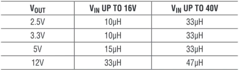
The calculated tOFF-TIME should be more than LT3470’s minimum tOFF-TIME (See Electrical Characteristics), so the application circuit is capable of delivering full rated output current. If the full output current of 200mA is not required, the calculated tOFF-TIME can be made less than minimum tOFF-TIME possibly allowing the use of a smaller inductor. See Table 1 for an inductor value selection guide.
Table 1. Recommended Inductors for Loads up to 200mA
VOUT VIN UP TO 16V VIN UP TO 40V
2.5V 10µH 33µH
3.3V 10µH 33µH
5V 15µH 33µH
12V 33µH 47µH
Choose an inductor that is intended for power applications. Table 2 lists several manufacturers and inductor series. For robust output short-circuit protection at high VIN (up to 40V) use at least a 33µH inductor with a minimum 450mA saturation current. If short-circuit performance is not required, inductors with ISAT of 300mA or more may
LT3470
10
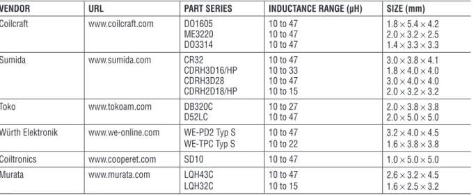
3470fdTable 2. Inductor Vendors
VENDOR URL PART SERIES INDUCTANCE RANGE (µH) SIZE (mm)
Coilcraft www.coilcraft.com DO1605 ME3220 DO3314 10 to 47 10 to 47 10 to 47 1.8 × 5.4 × 4.2 2.0 × 3.2 × 2.5 1.4 × 3.3 × 3.3 Sumida www.sumida.com CR32 CDRH3D16/HP CDRH3D28 CDRH2D18/HP 10 to 47 10 to 33 10 to 47 10 to 15 3.0 × 3.8 × 4.1 1.8 × 4.0 × 4.0 3.0 × 4.0 × 4.0 2.0 × 3.2 × 3.2 Toko www.tokoam.com DB320C D52LC 10 to 27 10 to 47 2.0 2.0 ×× 3.8 5.0 ×× 3.8 5.0 Würth Elektronik www.we-online.com WE-PD2 Typ S
WE-TPC Typ S 10 to 47 10 to 22 3.2 1.6 ×× 4.0 3.8 ×× 4.5 3.8 Coiltronics www.cooperet.com SD10 10 to 47 1.0 × 5.0 × 5.0 Murata www.murata.com LQH43C
LQH32C 10 to 47 10 to 15 2.6 1.6 ×× 3.2 2.5 ×× 4.5 3.2
applicaTions inForMaTion
be used. It is important to note that inductor saturation current is reduced at high temperatures—see inductor vendors for more information.
Input Capacitor
Step-down regulators draw current from the input sup-ply in pulses with very fast rise and fall times. The input capacitor is required to reduce the resulting voltage ripple at the VIN pin of the LT3470 and to force this switching current into a tight local loop, minimizing EMI. The input capacitor must have low impedance at the switching frequency to do this effectively. A 1µF to 2.2µF ceramic capacitor satisfies these requirements.
If the input source impedance is high, a larger value ca-pacitor may be required to keep input ripple low. In this case, an electrolytic of 10µF or more in parallel with a 1µF ceramic is a good combination. Be aware that the input capacitor is subject to large surge currents if the LT3470 circuit is connected to a low impedance supply, and that some electrolytic capacitors (in particular tantalum) must be specified for such use.
Output Capacitor and Output Ripple
The output capacitor filters the inductor’s ripple current and stores energy to satisfy the load current when the LT3470 is quiescent. In order to keep output voltage ripple low, the impedance of the capacitor must be low at the
LT3470’s switching frequency. The capacitor’s equivalent series resistance (ESR) determines this impedance. Choose one with low ESR intended for use in switching regulators. The contribution to ripple voltage due to the ESR is ap-proximately ILIM • ESR. ESR should be less than ~150mΩ. The value of the output capacitor must be large enough to accept the energy stored in the inductor without a large change in output voltage. Setting this voltage step equal to 1% of the output voltage, the output capacitor must be:
COUT>50 •L • ILIM VOUT 2
where ILIM is the top current limit with VFB = 0V (see Elec-trical Characteristics). For example, an LT3470 producing 3.3V with L = 33µH requires 22µF. The calculated value can be relaxed if small circuit size is more important than low output ripple.
Sanyo’s POSCAP series in B-case and provides very good performance in a small package for the LT3470. Similar performance in traditional tantalum capacitors requires a larger package (C-case). With a high quality capacitor filtering the ripple current from the inductor, the output voltage ripple is determined by the delay in the LT3470’s feedback comparator. This ripple can be reduced further by adding a small (typically 22pF) phase lead capacitor between the output and the feedback pin.
LT3470
11
3470fdapplicaTions inForMaTion
Ceramic Capacitors
Ceramic capacitors are small, robust and have very low ESR. However, ceramic capacitors can cause problems when used with the LT3470. Not all ceramic capacitors are suitable. X5R and X7R types are stable over temperature and applied voltage and give dependable service. Other types, including Y5V and Z5U have very large temperature and voltage coefficients of capacitance. In an application circuit they may have only a small fraction of their nominal capacitance resulting in much higher output voltage ripple than expected.
Ceramic capacitors are piezoelectric. The LT3470’s switch-ing frequency depends on the load current, and at light loads the LT3470 can excite the ceramic capacitor at audio frequencies, generating audible noise. Since the LT3470 operates at a lower current limit during Burst Mode opera-tion, the noise is typically very quiet to a casual ear. If this audible noise is unacceptable, use a high performance electrolytic capacitor at the output. The input capacitor can be a parallel combination of a 2.2µF ceramic capacitor and a low cost electrolytic capacitor.
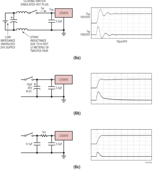
A final precaution regarding ceramic capacitors concerns the maximum input voltage rating of the LT3470. A ceramic input capacitor combined with trace or cable inductance forms a high quality (under damped) tank circuit. If the LT3470 circuit is plugged into a live supply, the input volt-age can ring to twice its nominal value, possibly exceeding the LT3470’s rating. This situation is easily avoided; see the Hot-Plugging Safely section.
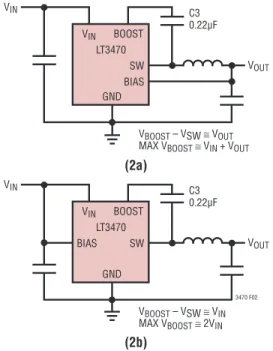
BOOST and BIAS Pin Considerations
Capacitor C3 and the internal boost Schottky diode (see Block Diagram) are used to generate a boost voltage that is higher than the input voltage. In most cases a 0.22µF capacitor will work well. Figure 2 shows two ways to ar-range the boost circuit. The BOOST pin must be more than 2.5V above the SW pin for best efficiency. For outputs of 3.3V and above, the standard circuit (Figure 2a) is best. For outputs between 2.5V and 3V, use a 0.47µF. For lower output voltages the boost diode can be tied to the input
Figure 2. Two Circuits for Generating the Boost Voltage
Table 3. Capacitor Vendors
VENDOR PHONE URL PART SERIES COMMENTS
Panasonic (714) 373-7366 www.panasonic.com Ceramic, Polymer, Tantalum
EEF Series Kemet (864) 963-6300 www.kemet.com Ceramic,
Tantalum T494, T495 Sanyo (408) 749-9714 www.sanyovideo.com Ceramic,
Polymer, Tantalum
POSCAP Murata (404) 436-1300 www.murata.com Ceramic
AVX www.avxcorp.com Ceramic,
Tantalum TPS Series Taiyo Yuden (864) 963-6300 www.taiyo-yuden.com Ceramic
VIN BOOST LT3470 (2a) (2b) SW C3 0.22µF VIN VOUT VBOOST – VSW ≅ VOUT
MAX VBOOST≅ VIN + VOUT
BIAS GND VIN BOOST LT3470 SW BIAS C3 0.22µF VIN VOUT 3470 F02 VBOOST – VSW ≅ VIN MAX VBOOST≅ 2VIN GND
LT3470
12
3470fdFigure 3. The Minimum Input Voltage Depends on Output Voltage, Load Current and Boost Circuit
Minimum Input Voltage, VOUT = 3.3V
Minimum Input Voltage, VOUT = 5V
Figure 4. Diode D1 Prevents a Shorted Input from Discharging a Backup Battery Tied to the Output; It Also Protects the Circuit from a Reversed Input. The LT3470 Runs Only When the Input Is Present Hot-Plugging Safely
applicaTions inForMaTion
(Figure 2b). The circuit in Figure 2a is more efficient because the BOOST pin current and BIAS pin quiescent current comes from a lower voltage source. You must also be sure that the maximum voltage ratings of the BOOST and BIAS pins are not exceeded.
The minimum operating voltage of an LT3470 application is limited by the undervoltage lockout (4V) and by the maximum duty cycle as outlined in a previous section. For proper start-up, the minimum input voltage is also limited by the boost circuit. If the input voltage is ramped slowly, or the LT3470 is turned on with its SHDN pin when the output is already in regulation, then the boost capacitor may not be fully charged. The plots in Figure 3 show minimum
VIN to start and to run. At light loads, the inductor current becomes discontinuous and the effective duty cycle can be very high. This reduces the minimum input voltage to approximately 300mV above VOUT. At higher load currents, the inductor current is continuous and the duty cycle is limited by the maximum duty cycle of the LT3470, requiring a higher input voltage to maintain regulation.
Shorted Input Protection
If the inductor is chosen so that it won’t saturate exces-sively at the top switch current limit maximum of 450mA, an LT3470 buck regulator will tolerate a shorted output even if VIN = 40V. There is another situation to consider in systems where the output will be held high when the input to the LT3470 is absent. This may occur in battery charging applications or in battery backup systems where a battery or some other supply is diode OR-ed with the LT3470’s output. If the VIN pin is allowed to float and the SHDN pin is held high (either by a logic signal or because it is tied to VIN), then the LT3470’s internal circuitry will pull its quiescent current through its SW pin. This is fine if your system can tolerate a few mA in this state. If you ground the SHDN pin, the SW pin current will drop to es-sentially zero. However, if the VIN pin is grounded while the output is held high, then parasitic diodes inside the LT3470 can pull large currents from the output through the SW pin and the VIN pin. Figure 4 shows a circuit that will run only when the input voltage is present and that protects against a shorted or reversed input.
LOAD CURRENT (mA) 0 3.0 INPUT VOLTAGE (V) 3.5 4.0 4.5 5.0 5.5 6.0 50 100 150 200 3470 G18 TA = 25°C V IN TO START VIN TO RUN
LOAD CURRENT (mA) 0 INPUT VOLTAGE (V) 6 7 200 3470 G19 5 4 50 100 150 8 TA = 25°C VIN TO START VIN TO RUN VIN BOOST LT3470 SOT-23 SW SHDN 3470 F04 VIN 100k D1 1M VOUT BACKUP BIAS FB GND
LT3470
13
3470fdapplicaTions inForMaTion
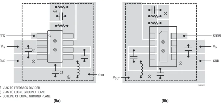
PCB Layout
For proper operation and minimum EMI, care must be taken during printed circuit board layout. Note that large, switched currents flow in the power switch, the internal catch diode and the input capacitor. The loop formed by these components should be as small as possible. Further-more, the system ground should be tied to the regulator ground in only one place; this prevents the switched cur-rent from injecting noise into the system ground. These components, along with the inductor and output capacitor, should be placed on the same side of the circuit board, and their connections should be made on that layer. Place a local, unbroken ground plane below these components, and tie this ground plane to system ground at one location,
ideally at the ground terminal of the output capacitor C2. Additionally, the SW and BOOST nodes should be kept as small as possible. Unshielded inductors can induce noise in the feedback path resulting in instability and increased output ripple. To avoid this problem, use vias to route the VOUT trace under the ground plane to the feedback divider (as shown in Figure 5). Finally, keep the FB node as small as possible so that the ground pin and ground traces will shield it from the SW and BOOST nodes. Figure 5 shows component placement with trace, ground plane and via locations. Include vias near the GND pin, or pad, of the LT3470 to help remove heat from the LT3470 to the ground plane.
Figure 5. A Good PCB Layout Ensures Proper, Low EMI Operation
SHDN VIN VOUT (5a) (5b) VOUT 3470 F05 GND SHDN VIN GND C1 C2
VIAS TO FEEDBACK DIVIDER VIAS TO LOCAL GROUND PLANE OUTLINE OF LOCAL GROUND PLANE
LT3470
14
3470fdapplicaTions inForMaTion
Hot-Plugging Safely
The small size, robustness and low impedance of ceramic capacitors make them an attractive option for the input bypass capacitor of LT3470. However, these capacitors can cause problems if the LT3470 is plugged into a live supply (see Linear Technology Application Note 88 for a complete discussion). The low loss ceramic capacitor combined with stray inductance in series with the power source forms an under damped tank circuit, and the voltage at the VIN pin of the LT3470 can ring to twice the nominal input voltage, possibly exceeding the LT3470’s rating and damaging the part. If the input supply is poorly controlled or the user will be plugging the LT3470 into an energized supply, the input network should be designed to prevent this overshoot. Figure 6 shows the waveforms that result when an LT3470 circuit is connected to a 24V supply through six feet of 24-gauge twisted pair. The first plot is the response with a 2.2µF ceramic capacitor at the input. The input voltage rings as high as 35V and the input current peaks at 20A. One method of damping the tank circuit is to add another capacitor with a series resistor to the circuit. In Figure 6b an aluminum electrolytic capacitor has been added. This capacitor’s high equivalent series resistance damps the circuit and eliminates the voltage overshoot. The extra capacitor improves low frequency ripple filtering and can slightly improve the efficiency of the circuit, though it is likely to be the largest component in the circuit. An alterna-tive solution is shown in Figure 6c. A 1Ω resistor is added in series with the input to eliminate the voltage overshoot
(it also reduces the peak input current). A 0.1µF capacitor improves high frequency filtering. This solution is smaller and less expensive than the electrolytic capacitor. For high input voltages its impact on efficiency is minor, reducing efficiency less than one half percent for a 5V output at full load operating from 24V.
High Temperature Considerations
The die junction temperature of the LT3470 must be lower than the maximum rating of 125°C (150°C for the H-grade). This is generally not a concern unless the ambi-ent temperature is above 85°C. For higher temperatures, care should be taken in the layout of the circuit to ensure good heat sinking of the LT3470. The maximum load current should be derated as the ambient temperature approaches the maximum junction rating. The die tem-perature is calculated by multiplying the LT3470 power dissipation by the thermal resistance from junction to ambient. Power dissipation within the LT3470 can be estimated by calculating the total power loss from an efficiency measurement. Thermal resistance depends on the layout of the circuit board and choice of package. The DD package with the exposed pad has a thermal resistance of approximately 80°C/W while the ThinSOT is approximately 150°C/W. Finally, be aware that at high ambient temperatures the internal Schottky diode will have significant leakage current (see Typical Performance Characteristics) increasing the quiescent current of the LT3470 converter.
LT3470
15
3470fdapplicaTions inForMaTion
Figure 6. A Well Chosen Input Network Prevents Input Voltage Overshoot and Ensures Reliable Operation When the LT3470 Is Connected to a Live Supply
+ LT3470 2.2µF VIN 10V/DIV IIN 10A/DIV 10µs/DIV VIN CLOSING SWITCH SIMULATES HOT PLUG
IIN (6a) (6b) (6c) LOW IMPEDANCE ENERGIZED 24V SUPPLY STRAY INDUCTANCE DUE TO 6 FEET (2 METERS) OF TWISTED PAIR + LT3470 2.2µF 10µF 35V AI.EI. LT3470 2.2µF 0.1µF 1Ω 3470 F06
LT3470
16
3470fd3.3V Step-Down Converter 5V Step-Down Converter
2.5V Step-Down Converter VIN BOOST LT3470 SW SHDN C3 0.22µF, 6.3V 22pF C2 22µF 3470 TA03 C1 1µF VIN 5.5V TO 40V VOUT 3.3V 200mA R1 324k R2 200k C1: TDK C3216JB1H105M C2: CE JMK316 BJ226ML-T L1: TOKO A993AS-270M=P3 L1 33µH BIAS FB GND OFF ON VIN BOOST LT3470 SW SHDN C3 0.22µF, 6.3V 22pF C2 22µF 3470 TA04 C1 1µF VIN 7V TO 40V VOUT 5V 200mA R1 604k R2 200k L1 33µH BIAS FB GND OFF ON C1: TDK C3216JB1H105M C2: CE JMK316 BJ226ML-T L1: TOKO A914BYW-330M=P3
Typical applicaTions
1.8V Step-Down Converter 12V Step-Down Converter VIN BOOST LT3470 SW SHDN C3 0.47µF, 6.3V 22pF C2 22µF 3470 TA07 C1 1µF VIN 4.7V TO 40V VOUT 2.5V 200mA R1 200k R2 200k C1: TDK C3216JB1H105M C2: TDK C2012JB0J226M L1: SUMIDA CDRH3D28 L1 33µH BIAS FB GND OFF ON VIN BOOST LT3470 SW SHDN BIAS C3 0.22µF, 25V 22pF C2 22µF 3470 TA05 C1 1µF VIN 4V TO 23V VOUT 1.8V 200mA R1 147k R2 332k L1 22µH FB GND OFF ON C1: TDK C3216JB1H105M C2: TDK C2012JB0J226M L1: MURATA LQH32CN150K53 VIN BOOST LT3470 SW SHDN C3 0.22µF, 16V 22pF C2 10µF 3470 TA06 C1 1µF VIN 15V TO 34V VOUT 12V 200mA R1 866k R2 100k C1: TDK C3216JB1H105M C2: TDK C3216JB1C106M L1: MURATA LQH32CN150K53 L1 33µH BIAS FB GND OFF ONLT3470
17
3470fdpackage DescripTion
TS8 Package 8-Lead Plastic TSOT-23
(Reference LTC DWG # 05-08-1637 Rev A) 1.50 – 1.75 (NOTE 4) 2.80 BSC 0.22 – 0.36 8 PLCS (NOTE 3) DATUM ‘A’ 0.09 – 0.20 (NOTE 3) TS8 TSOT-23 0710 REV A 2.90 BSC (NOTE 4) 0.65 BSC 1.95 BSC 0.80 – 0.90 1.00 MAX 0.01 – 0.10 0.20 BSC 0.30 – 0.50 REF PIN ONE ID NOTE:
1. DIMENSIONS ARE IN MILLIMETERS 2. DRAWING NOT TO SCALE
3. DIMENSIONS ARE INCLUSIVE OF PLATING
4. DIMENSIONS ARE EXCLUSIVE OF MOLD FLASH AND METAL BURR 5. MOLD FLASH SHALL NOT EXCEED 0.254mm
6. JEDEC PACKAGE REFERENCE IS MO-193 3.85 MAX
0.40
MAX 0.65REF
RECOMMENDED SOLDER PAD LAYOUT PER IPC CALCULATOR
1.4 MIN 2.62 REF
1.22 REF
LT3470
18
3470fdpackage DescripTion
DDB Package 8-Lead Plastic DFN (3mm × 2mm) (Reference LTC DWG # 05-08-1702 Rev B) 2.00 ±0.10 (2 SIDES) NOTE:1. DRAWING CONFORMS TO VERSION (WECD-1) IN JEDEC PACKAGE OUTLINE M0-229 2. DRAWING NOT TO SCALE
3. ALL DIMENSIONS ARE IN MILLIMETERS
4. DIMENSIONS OF EXPOSED PAD ON BOTTOM OF PACKAGE DO NOT INCLUDE MOLD FLASH. MOLD FLASH, IF PRESENT, SHALL NOT EXCEED 0.15mm ON ANY SIDE 5. EXPOSED PAD SHALL BE SOLDER PLATED
6. SHADED AREA IS ONLY A REFERENCE FOR PIN 1 LOCATION ON THE TOP AND BOTTOM OF PACKAGE
0.40 ± 0.10
BOTTOM VIEW—EXPOSED PAD 0.56 ± 0.05 (2 SIDES) 0.75 ±0.05 R = 0.115 TYP R = 0.05 TYP 2.15 ±0.05 (2 SIDES) 3.00 ±0.10 (2 SIDES) 1 4 8 5 PIN 1 BAR TOP MARK (SEE NOTE 6) 0.200 REF 0 – 0.05 (DDB8) DFN 0905 REV B 0.25 ± 0.05 2.20 ±0.05 (2 SIDES)
RECOMMENDED SOLDER PAD PITCH AND DIMENSIONS 0.61 ±0.05 (2 SIDES) 1.15 ±0.05 0.70 ±0.05 2.55 ±0.05 PACKAGE OUTLINE 0.25 ± 0.05 0.50 BSC PIN 1 R = 0.20 OR 0.25 × 45° CHAMFER 0.50 BSC
LT3470
19
3470fd Information furnished by Linear Technology Corporation is believed to be accurate and reliable.However, no responsibility is assumed for its use. Linear Technology Corporation makes no representa-tion that the interconnecrepresenta-tion of its circuits as described herein will not infringe on existing patent rights.
revision hisTory
REV DATE DESCRIPTION PAGE NUMBER
D 09/11 Corrected lead-based tape and reel part numbers in the Order Information section. 2
LT3470
20
Linear Technology Corporation
3470fd1630 McCarthy Blvd., Milpitas, CA 95035-7417
(408) 432-1900 ●FAX: (408) 434-0507 ● www.linear.com LINEAR TECHNOLOGY CORPORATION 2004
LT 0911 REV D • PRINTED IN USA
relaTeD parTs
PART NUMBER DESCRIPTION COMMENTS
LT1616 25V, 500mA (IOUT), 1.4MHz, High Efficiency
Step-Down DC/DC Converter VThinSOT PackageIN = 3.6V to 25V, VOUT = 1.25V, IQ = 1.9mA, ISD < 1µA, LT1676 60V, 440mA (IOUT), 100kHz, High Efficiency
Step-Down DC/DC Converter VS8 PackageIN = 7.4V to 60V, VOUT = 1.24V, IQ = 3.2mA, ISD = 2.5µA, LT1765 25V, 2.75A (IOUT), 1.25MHz, High Efficiency
Step-Down DC/DC Converter VS8, TSSOP16E PackagesIN = 3V to 25V, VOUT = 1.2V, IQ = 1mA, ISD = 15µA, LT1766 60V, 1.2A (IOUT), 200kHz, High Efficiency
Step-Down DC/DC Converter VTSSOP16/E PackageIN = 5.5V to 60V, VOUT = 1.2V, IQ = 2.5mA, ISD = 25µA, LT1767 25V, 1.2A (IOUT), 1.25MHz, High Efficiency
Step-Down DC/DC Converter VMS8/E PackagesIN = 3V to 25V; VOUT = 1.2V, IQ = 1mA, ISD = 6µA, LT1776 40V, 550mA (IOUT), 200kHz, High Efficiency
Step-Down DC/DC Converter VN8, S8 PackagesIN = 7.4V to 40V; VOUT = 1.24V, IQ = 3.2mA, ISD = 30µA, LTC®1877 600mA (I
OUT), 550kHz, Synchronous
Step-Down DC/DC Converter VMS8 PackageIN = 2.7V to 10V; VOUT = 0.8V, IQ = 10µA, ISD ≤ 1µA, LTC1879 1.2A (IOUT), 550kHz, Synchronous
Step-Down DC/DC Converter VTSSOP16 PackageIN = 2.7V to 10V; VOUT = 0.8V, IQ = 15µA, ISD ≤ 1µA, LT1933 36V, 600mA, 500kHz, High Efficiency
Step-Down DC/DC Converter V??? PackageIN = 3.6V to 36V; VOUT = 1.25V, IQ = 2.5µA, ISD ≤ 1µA, LT1934 34V, 250mA (IOUT), Micropower, Step-Down
DC/DC Converter V??? PackageIN = 3.2V to 34V; VOUT = 1.25V, IQ = 12µA, ISD ≤ 1µA, LT1956 60V, 1.2A (IOUT), 500kHz, High Efficiency
Step-Down DC/DC Converter VTSSOP16/E PackageIN = 5.5V to 60V, VOUT = 1.2V, IQ = 2.5mA, ISD = 25µA, LTC3405/LTC3405A 300mA (IOUT), 1.5MHz, Synchronous
Step-Down DC/DC Converter VThinSOT PackageIN = 2.7V to 6V, VOUT = 0.8V, IQ = 20µA, ISD ≤ 1µA, LTC3406/LTC3406B 600mA (IOUT), 1.5MHz, Synchronous
Step-Down DC/DC Converter VThinSOT PackageIN = 2.5V to 5.5V, VOUT = 0.6V, IQ = 20µA, ISD ≤ 1µA, LTC3411 1.25A (IOUT), 4MHz, Synchronous
Step-Down DC/DC Converter VMS PackageIN = 2.5V to 5.5V, VOUT = 0.8V, IQ = 60µA, ISD ≤ 1µA, LTC3412 2.5A (IOUT), 4MHz, Synchronous
Step-Down DC/DC Converter VTSSOP16E PackageIN = 2.5V to 5.5V, VOUT = 0.8V, IQ = 60µA, ISD ≤ 1µA, LTC3430 60V, 2.75A (IOUT), 200kHz, High Efficiency