VCNL4020X01
www.vishay.com
Vishay Semiconductors
Fully Integrated Proximity and Ambient Light Sensor with
Infrared Emitter, I
2
C Interface, and Interrupt Function
DESCRIPTION
The VCNL4020X01 is a fully integrated proximity and
ambient light sensor. Fully integrated means that the
infrared emitter is included in the package. It has 16 bit
resolution. It includes a signal processing IC and features
standard I
2C communication interface. It features an
interrupt function.
APPLICATIONS
• Proximity sensor for:
-
Mobile devices
(e.g. smart phones, touch phones,
PDAs, GPS) for touch screen locking, power saving etc.
-
Automotive
for presence detection
• Integrated ambient light function for display / keypad
contrast control and dimming of mobile devices
• Rear view mirror dimming in automotive
• Proximity
/
optical switch for consumer, computing,
automotive and industrial devices, and displays (like
notebooks, tablet PCs, and automotive touch panels)
• Dimming control for consumer, computing, industrial, and
automotive displays
FEATURES
• Package type: surface mount
• Dimensions (L x W x H in mm):
4.90 x 2.40 x 0.83
• AEC-Q101 qualified
• Integrated modules: infrared emitter (IRED),
ambient light sensor (ALS-PD), proximity
sensor (PD), and signal conditioning IC
• Interrupt function
• Supply voltage range V
DD: 2.5 V to 3.6 V
• Supply voltage range IR anode: 2.5 V to 5 V
• Communication via I
2C interface
• I
2C bus H-level range: 1.7 V to 5 V
• Floor life: 168 h, MSL 3, according to J-STD-020
• Low stand by current consumption: 1.5 μA
• Material categorization: for definitions of compliance
please see
www.vishay.com/doc?99912
PROXIMITY FUNCTION
• Built-in infrared emitter and photo-pin-diode for proximity
function
• 16 bit effective resolution for proximity detection range
ensures excellent cross talk immunity
• Programmable LED drive current from 10 mA to 200 mA in
10 mA steps
• Excellent ambient light suppression by signal modulation
• Proximity distance up to 200 mm
AMBIENT LIGHT FUNCTION
• Built-in ambient light photo-pin-diode with close-to-
human-eye sensitivity
• 16 bit dynamic range from 0.25 lx to 16 klx
• 100 Hz and 120 Hz flicker noise rejection
7 nc 6 nc 9 GND 8 GND 10 IR cathode IR anode 1 SDA 2 INT 3 SCL 4 VDD 5 22620
PRODUCT SUMMARY
VCNL4020X01
www.vishay.com
Vishay Semiconductors
Rev. 1.2, 13-Aug-14 Document Number: 84177
Notes
(1) MOQ: minimum order quantity
(2) A sensor starter kit is available, along with an add-on demo board for each of the sensors.
Please visit www.vishay.com/moreinfo/vcnldemokit/ for more information.
Contact any catalog distributor or a local Vishay sales representative to purchase the sensor starter kit and contact [email protected] to receive an add-on sensor board.
ORDERING INFORMATION
ORDERING CODE PACKAGING VOLUME (1) REMARKS
VCNL4020X01-GS08
Tape and reel MOQ: 3300 pcs 4.90 mm x 2.40 mm x 0.83 mm
VCNL4020X01-GS18 MOQ: 13 000 pcs
Sensor starter kit (2) - MOQ: 1 pc
-ABSOLUTE MAXIMUM RATINGS
(T
amb= 25 °C, unless otherwise specified)
PARAMETER TEST CONDITION SYMBOL MIN. MAX. UNIT
Supply voltage VDD -0.3 5.5 V
Operation temperature range Tamb -40 +105 °C
Storage temperature range Tstg -40 +105 °C
Total power dissipation Tamb≤ 25 °C Ptot 50 mW
Junction temperature Tj 105 °C
BASIC CHARACTERISTICS
(T
amb= 25 °C, unless otherwise specified)
PARAMETER TEST CONDITION SYMBOL MIN. TYP. MAX. UNIT
Supply voltage VDD 2.5 3.6 V
Supply voltage IR anode 2.5 5 V
I2C Bus H-level range 1.7 5 V
INT H-level range 1.7 5 V
INT low voltage 3 mA sink current 0.4 V
Current consumption Standby current,
no IRED-operation 1.5 2 μA
Current consumption proximity mode incl. IRED (averaged)
2 measurements per second,
IRED current 20 mA 5 μA
250 measurements per second,
IRED current 20 mA 520 μA
2 measurements per second,
IRED current 200 mA 35 μA
250 measurements per second,
IRED current 200 mA 4 mA
Current consumption ambient light mode
2 measurements per second
averaging = 1 2.5 μA
8 measurements per second
averaging = 1 10 μA
2 measurements per second
averaging = 64 160 μA
8 measurements per second
averaging = 64 640 μA
Ambient light resolution Digital resolution (LSB count) 0.25 lx
Ambient light output EV = 100 lx
averaging = 64 400 counts
I2C clock rate range f
VCNL4020X01
www.vishay.com
Vishay Semiconductors
CIRCUIT BLOCK DIAGRAM
Note
• nc must not be electrically connected
Pads 6 and 7 are only considered as solder pads
TEST CIRCUIT
BASIC CHARACTERISTICS
(T
amb= 25 °C, unless otherwise specified)
Fig. 1 - Idle Current vs. Ambient Temperature Fig. 3 - Proximity Value vs. Distance
22621 10 IR cathode 9 GND 8 GND 6 nc 7 nc IR anode 1 SDA 2 INT 3 SCL 4 VDD 5 IRED VCNL 4020 ASIC Ambi PD Proxi PD d = 20 mm
Kodak gray card (18 % reflectivity) VCNL4020X01 IRED 30 mm x 30 mm Proxi-PD 2.8 1.0 1.2 1.4 1.8 1.6 2.0 2.2 100 -75 -50 -25 0 25 50 75 IDD - S
upply Current Idle Mode (μA)
Tamb - Ambient Temperature (°C)
2.6 2.4 VDD = 3.6 V VDD = 3.5 V VDD = 3.3 V VDD = 3.1 V VDD = 2.9 V VDD = 2.7 V VDD = 2.5 V 2.8 1.2 1.4 1.6 1.8 2.0 2.2 - S
upply Current Idle Mode (μA)
100 °C 80 °C 55 °C 25 °C -10 °C -40 °C 2.6 2.4 100 000 1 100 1000 10 000 10 0.1 1 10 100 Proximity Value (ct s )
Distance to Reflecting Card (mm)
200 mA
Media: Kodak gray card
20 mA 100 mA 260 20 40 60 200 IIRED
- Forward Current IRED (mA)
20 mA 40 mA 60 mA 80 mA 100 mA 120 mA 140 mA 160 mA 180 mA 200 mA VIRED = 2.5 V 240 220 180 160 140 120 100 80
VCNL4020X01
www.vishay.com
Vishay Semiconductors
Rev. 1.2, 13-Aug-14 Document Number: 84177
Fig. 5 - Relative Radiant Intensity vs. Wavelength
Fig. 6 - Relative Radiant Intensity vs. Angular Displacement
Fig. 7 - Relative Spectral Sensitivity vs. Wavelength (Proximity Sensor)
Fig. 8 - Relative Radiant Sensitivity vs. Angular Displacement (Proximity Sensor)
Fig. 9 - Ambient Light Value vs. Illuminance
Fig. 10 - Relative Spectral Sensitivity vs. Wavelength (Ambient Light Sensor)
1.1 0 0.2 0.4 0.6 0.8 0.9 1.0 0.1 0.3 0.5 0.7 1050 750 800 850 900 950 1000 Ie, rel
- Relative Radiant Inten
s ity λ - Wavelength (nm) 22305 IF = 100 mA 0° 20° 40° 60° 80° 0.6 0.7 0.8 0.9 1.0 0 0.1 0.2 0.3 0.4 0.5 Irel
- Relative Radiant Inten
s ity 22306 ϕ - Angular Displacement 1.1 0 0.2 0.4 0.6 0.8 0.9 1.0 0.1 0.3 0.5 0.7 1100 400 500 600 700 800 900 1000 S ( λ )rel - Relative S pectral S en s itivity λ - Wavelength (nm) 22307 0° 20° 40° 60° 80° 0.6 0.7 0.8 0.9 1.0 0 0.1 0.2 0.3 0.4 0.5 Srel - Relative S en s itivity 22308 ϕ - Angular Displacement 100 000 1 100 1000 10 000 10 Ambient Light S ignal (ct s ) EV - Illuminance (lx) 0.1 1 10 100 1000 10 000 0 0.2 0.4 0.6 0.8 1.0 1100 400 500 600 700 800 900 1000 S ( λ )rel - Relative S pectral S en s itivity λ - Wavelength (nm) VCNL4020X01 Human eye
VCNL4020X01
www.vishay.com
Vishay Semiconductors
Fig. 11 - Relative Radiant Sensitivity vs. Angular Displacement (Ambient Light Sensor)
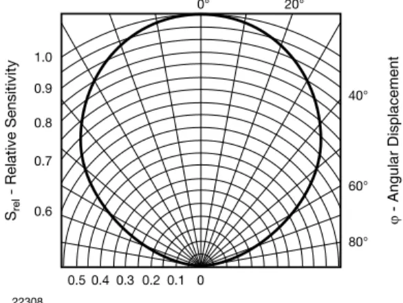
APPLICATION INFORMATION
VCNL4020X01 is a cost effective solution of proximity and ambient light sensor with I
2C bus interface. The standard serial digital
interface is easy to access “Proximity Signal” and “Light Intensity” without complex calculation and programming by external
controller. Beside the digital output also a flexible programmable interrupt pin is available.
1. Application Circuit
Fig. 12 - Application Circuit (x) = Pin Number
Notes
• The interrupt pin is an open drain output. The needed pull-up resistor may be connected to the same supply voltage as the application controller and the pull-up resistors at SDA/SCL. Proposed value R2 should be >1 kΩ , e.g. 10 kΩ to 100 kΩ.
Proposed value for R3 and R4, e.g. 2.2 kΩ to 4.7 kΩ, depend also on the I2C bus speed.
For detailed description about set-up and use of the interrupt as well as more application related information see AN: “Designing VCNL3020 into an Application”.
• IR_Cathode needs no external connection. The needed connection to the driver is done internally.
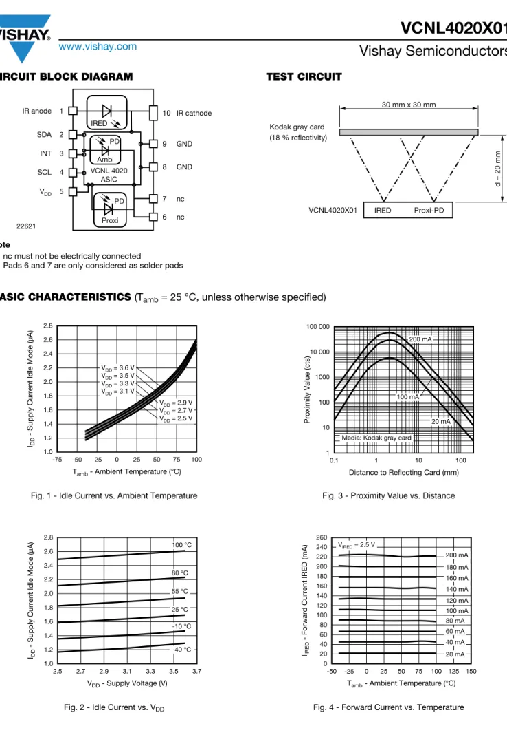
0° 20° 40° 60° 80° 0.6 0.7 0.8 0.9 1.0 0 0.1 0.2 0.3 0.4 0.5 Srel - Relative S en s itivity 22311 Vertical Horizontal ϕ - Angular Displacement
Ho
s
t
Micro Controller
I2C Bus Clock SCLI2C Bus Data SDA
INT (3) SCL (4) SDA (2) GND (8, 9) VDD (5) IR_Anode (1) C1 C2 C3 C4 R1 100 nF 100 nF 10 μF 22 μF 10R GPIO 2.5 V to 3.6 V 2.5 V to 5.0 V 1.7 V to 5.0 V R2 R3 R4
VCNL4020X01
VCNL4020X01
www.vishay.com
Vishay Semiconductors
Rev. 1.2, 13-Aug-14 Document Number: 84177
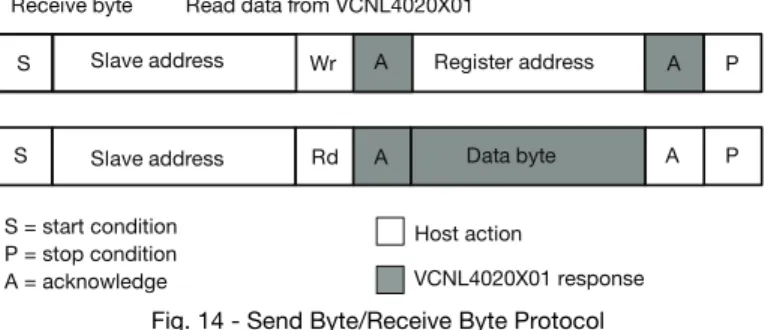
2. I
2C Interface
The VCNL4020X01 contains seventeen 8 bit registers for operation control, parameter setup and result buffering. All registers
are accessible via I
2C communication. Figure 13 shows the basic I
2C communication with VCNL4020X01.
The built in I
2C interface is compatible with all I
2C modes (standard, fast and high speed).
I
2C H-level range = 1.7 V to 5 V.
Please refer to the I
2C specification from NXP for details.
Fig. 13 - Send Byte/Receive Byte Protocol
Device Address
The VCNL4020X01 has a fix slave address for the host
programming and accessing selection. The predefined
7 bit I
2C bus address is set to 0010 011 = 13h. The least
significant bit (LSB) defines read or write mode. Accordingly
the bus address is set to 0010 011x = 26h for write, 27h for
read.
Register Addresses
VCNL4020X01 has seventeen user accessible 8 bit
registers. The register addresses are 80h (register #0) to 90h
(register #16).
REGISTER FUNCTIONS
Register #0 Command Register
Register address = 80h
The register #0 is for starting ambient light or proximity measurements. This register contains 2 flag bits for data ready indication.
Note
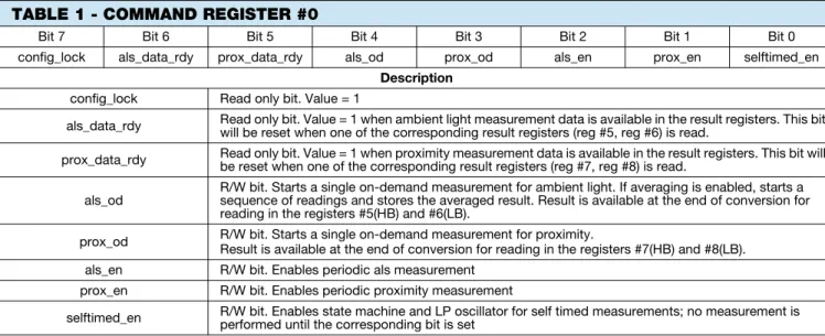
• With setting bit 3 and bit 4 at the same write command, a simultaneously measurement of ambient light and proximity is done. Beside als_en and/or prox_en first selftimed_en needs to be set. On-demand measurement modes are disabled if selftimed_en bit is set. For the selftimed_en mode changes in reading rates (reg #4 and reg #2) can be made only when b0 (selftimed_en bit) = 0. For the als_od mode changes to the reg #4 can be made only when b4 (als_od bit) = 0; this is to avoid synchronization problems and undefined states between the clock domains. In effect this means that it is only reasonable to change rates while no selftimed conversion is ongoing.
S Slave address
Rd
Receive byte Read data from VCNL4020X01
A Register address A
Wr P
S Slave address A Data byte A P Send byte Write command to VCNL4020X01
S = start condition P = stop condition A = acknowledge
Host action
VCNL4020X01 response
S Slave address Wr A Register address A Data byte A P
TABLE 1 - COMMAND REGISTER #0
Bit 7 Bit 6 Bit 5 Bit 4 Bit 3 Bit 2 Bit 1 Bit 0
config_lock als_data_rdy prox_data_rdy als_od prox_od als_en prox_en selftimed_en
Description
config_lock Read only bit. Value = 1
als_data_rdy Read only bit. Value = 1 when ambient light measurement data is available in the result registers. This bit will be reset when one of the corresponding result registers (reg #5, reg #6) is read. prox_data_rdy Read only bit. Value = 1 when proximity measurement data is available in the result registers. This bit will be reset when one of the corresponding result registers (reg #7, reg #8) is read.
als_od
R/W bit. Starts a single on-demand measurement for ambient light. If averaging is enabled, starts a sequence of readings and stores the averaged result. Result is available at the end of conversion for reading in the registers #5(HB) and #6(LB).
prox_od R/W bit. Starts a single on-demand measurement for proximity.
Result is available at the end of conversion for reading in the registers #7(HB) and #8(LB). als_en R/W bit. Enables periodic als measurement
prox_en R/W bit. Enables periodic proximity measurement
VCNL4020X01
www.vishay.com
Vishay Semiconductors
Register #1 Product ID Revision Register
Register address = 81h. This register contains information about product ID and product revision.
Register data value of current revision = 21h.
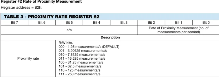
Register #2 Rate of Proximity Measurement
Register address = 82h.
Note
• If self_timed measurement is running, any new value written in this register will not be taken over until the mode is actualy cycled.
Register #3 LED Current Setting for Proximity Mode
Register address = 83h. This register is to set the LED current value for proximity measurement.
The value is adjustable in steps of 10 mA from 0 mA to 200 mA.
This register also contains information about the used device fuse program ID.
TABLE 2 - PRODUCT ID REVISION REGISTER #1
Bit 7 Bit 6 Bit 5 Bit 4 Bit 3 Bit 2 Bit 1 Bit 0
Product ID Revision ID
Description
Product ID Read only bits. Value = 2 Revision ID Read only bits. Value = 1
TABLE 3 - PROXIMITY RATE REGISTER #2
Bit 7 Bit 6 Bit 5 Bit 4 Bit 3 Bit 2 Bit 1 Bit 0
n/a Rate of Proximity Measurement (no. of measurements per second)
Description Proximity rate R/W bits. 000 - 1.95 measurements/s (DEFAULT) 001 - 3.90625 measurements/s 010 - 7.8125 measurements/s 011 - 16.625 measurements/s 100 - 31.25 measurements/s 101 - 62.5 measurements/s 110 - 125 measurements/s 111 - 250 measurements/s
TABLE 4 - IR LED CURRENT REGISTER #3
Bit 7 Bit 6 Bit 5 Bit 4 Bit 3 Bit 2 Bit 1 Bit 0
Fuse prog ID IR LED current value
Description
Fuse prog ID Read only bits.
Information about fuse program revision used for initial setup/calibration of the device. IR LED current value
R/W bits. IR LED current = Value (dec.) x 10 mA.
Valid Range = 0 to 20d. e.g. 0 = 0 mA , 1 = 10 mA, …., 20 = 200 mA (2 = 20 mA = DEFAULT) LED Current is limited to 200 mA for values higher as 20d.
VCNL4020X01
www.vishay.com
Vishay Semiconductors
Rev. 1.2, 13-Aug-14 Document Number: 84177
Register #4 Ambient Light Parameter Register
Register address = 84h.
Note
• If self_timed measurement is running, any new value written in this register will not be taken over until the mode is actualy cycled.
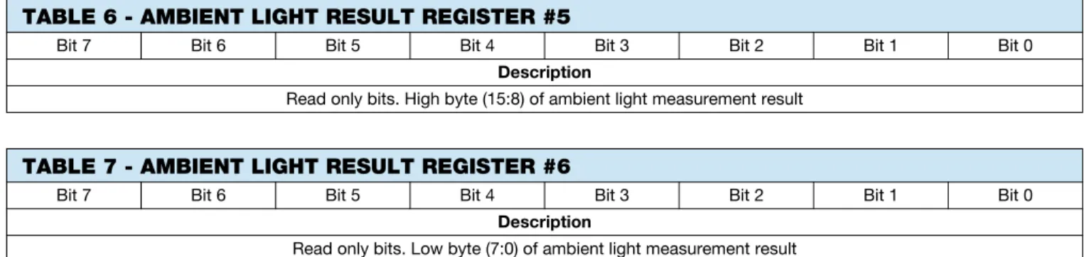
Register #5 and #6 Ambient Light Result Register
Register address = 85h and 86h. These registers are the result registers for ambient light measurement readings.
The result is a 16 bit value. The high byte is stored in register #5 and the low byte in register #6.
TABLE 5 - AMBIENT LIGHT PARAMETER REGISTER #4
Bit 7 Bit 6 Bit 5 Bit 4 Bit 3 Bit 2 Bit 1 Bit 0
Cont. conv.
mode als_rate
Auto offset compensation
Averaging function (number of measurements per run)
Description
Cont. conversion mode
R/W bit. Continuous conversion mode. Enable = 1; Disable = 0 = DEFAULT
This function can be used for performing faster ambient light measurements. This mode should only be used with ambient light on-demand measurements. Do not use with self-timed mode. Please refer to the application information chapter 3.3 for details about this function.
Ambient light measurement rate
R/W bits. Ambient light measurement rate 000 - 1 samples/s 001 - 2 samples/s = DEFAULT 010 - 3 samples/s 011 - 4 samples/s 100 - 5 samples/s 101 - 6 samples/s 110 - 8 samples/s 111 - 10 samples/s
Auto offset compensation
R/W bit. Automatic offset compensation. Enable = 1 = DEFAULT; Disable = 0
In order to compensate a technology, package or temperature related drift of the ambient light values there is a built in automatic offset compensation function.
With active auto offset compensation the offset value is measured before each ambient light measurement and subtracted automatically from actual reading.
Averaging function
R/W bits. Averaging function.
Bit values sets the number of single conversions done during one measurement cycle. Result is the average value of all conversions.
Number of conversions = 2decimal_value e.g. 0 = 1 conv., 1 = 2 conv, 2 = 4 conv., ….7 = 128 conv.
DEFAULT = 32 conv. (bit 2 to bit 0: 101)
TABLE 6 - AMBIENT LIGHT RESULT REGISTER #5
Bit 7 Bit 6 Bit 5 Bit 4 Bit 3 Bit 2 Bit 1 Bit 0
Description
Read only bits. High byte (15:8) of ambient light measurement result
TABLE 7 - AMBIENT LIGHT RESULT REGISTER #6
Bit 7 Bit 6 Bit 5 Bit 4 Bit 3 Bit 2 Bit 1 Bit 0
Description
VCNL4020X01
www.vishay.com
Vishay Semiconductors
Register #7 and #8 Proximity Measurement Result Register
Register address = 87h and 88h. These registers are the result registers for proximity measurement readings.
The result is a 16 bit value. The high byte is stored in register #7 and the low byte in register #8.
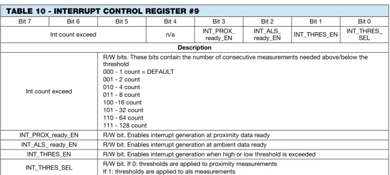
Register #9 Interrupt Control Register
Register address = 89h.
TABLE 8 - PROXIMITY RESULT REGISTER #7
Bit 7 Bit 6 Bit 5 Bit 4 Bit 3 Bit 2 Bit 1 Bit 0
Description
Read only bits. High byte (15:8) of proximity measurement result
TABLE 9 - PROXIMITY RESULT REGISTER #8
Bit 7 Bit 6 Bit 5 Bit 4 Bit 3 Bit 2 Bit 1 Bit 0
Description
Read only bits. Low byte (7:0) of proximity measurement result
TABLE 10 - INTERRUPT CONTROL REGISTER #9
Bit 7 Bit 6 Bit 5 Bit 4 Bit 3 Bit 2 Bit 1 Bit 0
Int count exceed n/a INT_PROX_
ready_EN INT_ALS_ ready_EN INT_THRES_EN INT_THRES_ SEL Description
Int count exceed
R/W bits. These bits contain the number of consecutive measurements needed above/below the threshold 000 - 1 count = DEFAULT 001 - 2 count 010 - 4 count 011 - 8 count 100 -16 count 101 - 32 count 110 - 64 count 111 - 128 count
INT_PROX_ready_EN R/W bit. Enables interrupt generation at proximity data ready INT_ALS_ ready_EN R/W bit. Enables interrupt generation at ambient data ready
INT_THRES_EN R/W bit. Enables interrupt generation when high or low threshold is exceeded INT_THRES_SEL R/W bit. If 0: thresholds are applied to proximity measurements
VCNL4020X01
www.vishay.com
Vishay Semiconductors
Rev. 1.2, 13-Aug-14 Document Number: 84177
Register #10 and #11 Low Threshold
Register address = 8Ah and 8Bh. These registers contain the low threshold value. The value is a 16 bit word. The high byte is
stored in register #10 and the low byte in register #11.
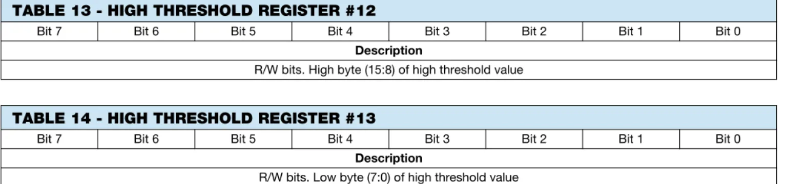
Register #12 and #13 High Threshold
Register address = 8Ch and 8Dh. These registers contain the high threshold value. The value is a 16 bit word. The high byte is
stored in register #12 and the low byte in register #13.
Register #14 Interrupt Status Register
Register address = 8Eh. This register contains information about the interrupt status for either proximity or ALS function and
indicates if high or low going threshold exceeded.
Note
• Once an interrupt is generated the corresponding status bit goes to 1 and stays there unless it is cleared by writing a 1 in the corresponding bit. The int pad will be pulled down while at least one of the status bit is 1.
TABLE 11 - LOW THRESHOLD REGISTER #10
Bit 7 Bit 6 Bit 5 Bit 4 Bit 3 Bit 2 Bit 1 Bit 0
Description
R/W bits. High byte (15:8) of low threshold value
TABLE 12 - LOW THRESHOLD REGISTER #11
Bit 7 Bit 6 Bit 5 Bit 4 Bit 3 Bit 2 Bit 1 Bit 0
Description
R/W bits. Low byte (7:0) of low threshold value
TABLE 13 - HIGH THRESHOLD REGISTER #12
Bit 7 Bit 6 Bit 5 Bit 4 Bit 3 Bit 2 Bit 1 Bit 0
Description
R/W bits. High byte (15:8) of high threshold value
TABLE 14 - HIGH THRESHOLD REGISTER #13
Bit 7 Bit 6 Bit 5 Bit 4 Bit 3 Bit 2 Bit 1 Bit 0
Description
R/W bits. Low byte (7:0) of high threshold value
TABLE 15 - INTERRUPT STATUS REGISTER #14
Bit 7 Bit 6 Bit 5 Bit 4 Bit 3 Bit 2 Bit 1 Bit 0
n/a int_prox_ready int_als_ready int_th_low int_th_hi
Description
int_prox_ready R/W bit. Indicates a generated interrupt for proximity int_als_ready R/W bit. Indicates a generated interrupt for als
int_th_low R/W bit. Indicates a low threshold exceed int_th_hi R/W bit. Indicates a high threshold exceed
VCNL4020X01
www.vishay.com
Vishay Semiconductors
Register #15 Proximity Modulator Timing Adjustment
Register address = 8Fh.
Note
• The settings for best performance will be provided by Vishay. With first samples this is evaluated to:
Delay Time = 0 ; Dead Time = 1 and Prox Frequency = 0 . With that register#15 should be programmed with 1 (= default value).
Register #16 Ambient IR Light Level Register
Register address = 90h.
This register is not intended to be used by customer.
3. IMPORTANT APPLICATION HINTS AND EXAMPLES
3.1 Receiver standby mode
In standby mode the receiver has the lowest current consumption of about 1.5 μA. In this mode only the I
2C interface is active.
This is always valid, when there are no measurement demands for proximity and ambient light executed. Also the current sink
for the IR-LED is inactive, so there is no need for changing register #3 (IR LED current).
3.2 Data Read
In order to get a certain register value, the register has to be addressed without data like shown in the following scheme. After
this register addressing, the data from the addressed register is written after a subsequent read command.
Fig. 14 - Send Byte/Receive Byte Protocol
TABLE 16 - PROXIMITY MODULATOR TIMING ADJUSTMENT #15
Bit 7 Bit 6 Bit 5 Bit 4 Bit 3 Bit 2 Bit 1 Bit 0
Modulation delay time Proximity frequency Modulation dead time
Description
Modulation delay time
R/W bits. Setting a delay time between IR LED signal and IR input signal evaluation.
This function is for compensation of delays from IR LED and IR photo diode. Also in respect to the possibility for setting different proximity signal frequency. Correct adjustment is optimizing measurement signal level. ( DEFAULT = 0)
Proximity frequency
R/W bits. Setting the proximity IR test signal frequency
The proximity measurement is using a square IR signal as measurement signal. Four different values are possible:
00 = 390.625 kHz (DEFAULT) 01 = 781.25 kHz
10 = 1.5625 MHz 11 = 3.125 MHz Modulation dead time
R/W bits. Setting a dead time in evaluation of IR signal at the slopes of the IR signal. ( DEFAULT = 1) This function is for reducing of possible disturbance effects.
This function is reducing signal level and should be used carefully.
S Slave address
Rd
Receive byte Read data from VCNL4020X01
A Register address A
Wr P
S Slave address A Data byte A P
S = start condition
P = stop condition
A = acknowledge
Host action
VCNL4020X01
www.vishay.com
Vishay Semiconductors
Rev. 1.2, 13-Aug-14 Document Number: 84177
Example: read register “Ambient Light Result Register” #5 and #6:
Addressing:
command: 26h, 85h (VCNL4020X01_I
2C_Bus_Write_Adr., Ambient Light Result Register #5 [85])
Read register #5: command: 27h, data (VCNL4020X01_I
2C_Bus_Read_Adr., {High Byte Data of Ambient Light Result register
#5 [85])}
Read register #6: command: 27h, data (VCNL4020X01_I
2C_Bus_Read_Adr., {Low Byte Data of Ambient Light Result register
#6 [86])}
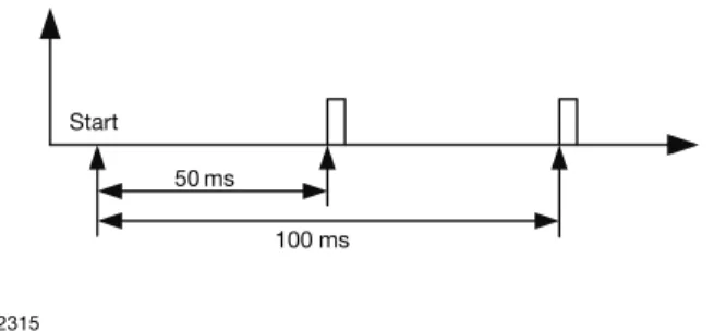
3.3 Continuous Conversion Mode in Ambient Light Measurement
In the following is a detail description of the function “continuous conversion” (bit 7 of register #4)
Standard mode (bit 7 of reg #4 = 0):
In standard mode the ambient light measurement is done during a fixed time frame of 100 ms. The single measurement itself
takes actually only appr. 300 μs.
The following figures show examples of this measurement timing in standard mode using averaging function 2 and 8 as
examples for illustration (possible values up to 128).
Fig. 15 - Ambient Light Measurement with Averaging = 2; Final Measurement Result = Average of these 2 Measurements
Fig. 16 - Ambient Light Measurement with Averaging = 8; Final Measurement Result = Average of these 8 Measurements
Note
• ≥ Independent of setting of averaging the result is available only after 100 ms.
Continuous conversion mode (bit 7 of register #4 = 1):
In continuous conversion mode the single measurements are done directly subsequent after each other.
See following examples in figure 17 and 18
Fig. 17 - Ambient Light Measurement with Averaging = 2; using Continuous Conversion Mode
Fig. 18 - Ambient Light Measurement with Averaging = 8; using Continuous Conversion Mode
50 ms 100 ms Start 22315 12.5 ms Start 100 ms 22316 460 μs Start 1.5 ms 22317 460 μs Start 4.2 ms 22318
VCNL4020X01
www.vishay.com
Vishay Semiconductors
PACKAGE DIMENSIONS
in millimeters
Not indicated tolerances ± 0.1
1
.2
7
1
.5
0.69
2.03
4.15
4.9
2
.4
0
.1
5
0
.8
3
0.65
0.685
2.74
4x0.685=
0.78
1.49
1.62
Drawing-No.: 6.550-5319Proposed PCB Footprint
Pinning Bottom view
Pinning Top view
0.3
0
.5
5
Ano d e E m it te r S D A IN T S C L V D D C a th o d e E m it te r V S S C a th o d e P D S D A IN T S C L V D D C a th o d e E m it te r V S S C a th o d e P D A n o d e E m it te r technical drawings according to DIN specifications0
.2
0
.8
2.74
4x 0.685=
2
.4
(
)
4.9
(
)
0.45
0
.2
0
.8
0.4
0.37
0.83
1.75
0.4
1.1
0.25
0.28
0.4
0.73
0.95
0.98
0
.2
4
VCNL4020X01
www.vishay.com
Vishay Semiconductors
Rev. 1.2, 13-Aug-14 Document Number: 84177
VCNL4020X01
www.vishay.com
Vishay Semiconductors
SOLDER PROFILE
Fig. 19 - Lead (Pb)-free Reflow Solder Profile according to J-STD-020
DRYPACK
Devices are packed in moisture barrier bags (MBB) to
prevent the products from moisture absorption during
transportation and storage. Each bag contains a desiccant.
FLOOR LIFE
Floor life (time between soldering and removing from MBB)
must not exceed the time indicated on MBB label:
Floor life: 168 h
Conditions: T
amb< 30 °C, RH < 60 %
Moisture sensitivity level 3, according to J-STD-020.
DRYING
In case of moisture absorption devices should be baked
before soldering. Conditions see J-STD-020 or label.
Devices taped on reel dry using recommended conditions
192 h at 40 °C (+ 5 °C), RH < 5 %.
0 50 100 150 200 250 300 0 50 100 150 200 250 300 Time (s) Temperature (°C) 240 °C 245 °C max. 260 °C max. 120 s max. 100 s 217 °C max. 30 smax. ramp up 3 °C/s max. ramp down 6 °C/s
19841
Legal Disclaimer Notice
www.vishay.com
Vishay
Revision: 13-Jun-16 Document Number: 91000