N e v e r s t o p t h i n k i n g .
Au t o m o t i v e P o w e r
MOSFET Power Losses
Calculation Using the
Data-Sheet Parameters
b y D r . D u š a n G r a o v a c , M a r c o P ü r s c h e l ,
A n d r e a s K i e p
MOSFET Converter Losses
Table of Content
1 Abstract...3
2 MOSFET and Diode Losses ...3
2.1 Conduction Losses...3
2.1.1 RDSon - Taking the Temperature and Production Variations into Account...5
2.2 Switching Losses ...6
2.2.1 Switch-on transient...6
2.2.2 Switch-off transient...9
2.2.3 Switching Energies and Losses ...10
2.3 Loss Balance...10
3 Application Specific Parameters ...11
3.1 Step-down (Buck) Converter...11
3.2 Step-up (Boost) Converter ...12
3.3 DC Motor Drive...13
3.4 Three-Phase AC Motor Drive...16
3.5 Switched Reluctance Motor Drive ...18
3.6 Piezo-Electric Actuator...19
4 Conclusion...20
MOSFET Converter Losses
1 Abstract
The aim of this Application Note is to provide a mathematical tool for the calculation of power losses in MOSFET-based power electronics converters used in automotive applications. After a general discussion on power losses calculation using the data-sheet parameters, the typical applications will be reviewed in order to extract the application specific parameters important for the loss balance.
2
MOSFET and Diode Losses
Power losses (Pl) in any component operating in the switch-mode can be divided in three groups:
a) Conduction losses (Pc)
b) Switching losses (Psw)
c) Blocking (leakage) losses (Pb), normally being neglected
Therefore: sw c b sw c l
P
P
P
P
P
P
=
+
+
≈
+
2.1 Conduction
Losses
Conduction losses in power MOSFET can be calculated using an MOSFET-approximation with the drain-source on-state resistance (RDSon):
D D DSon D DS
i
R
i
i
u
(
)
=
(
)
⋅
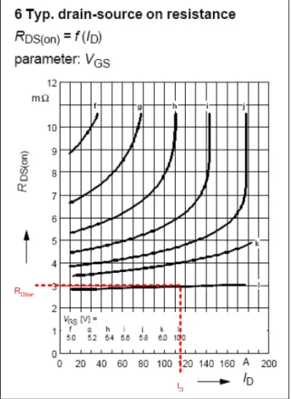
uDS and iD are drain-source voltage and the drain current, respectively. The typical RDSon can be read from
the data-sheet diagram, as shown in Fig. 1, where ID is the MOSFET on-state current as defined by the
application.
MOSFET Converter Losses
Therefore, the instantaneous value of the MOSFET conduction losses is:
)
(
)
(
)
(
)
(
t
u
t
i
t
R
i
2t
p
CM=
DS⋅
D=
DSon⋅
DIntegration of the instantaneous power losses over the switching cycle gives an average value of the MOSFET conduction losses:
2 0 2 0
))
(
(
1
)
(
1
Drms DSon Tsw D DSon sw Tsw CM sw CMR
i
t
dt
R
I
T
dt
t
p
T
P
=
∫
=
∫
⋅
=
⋅
where IDrms is the rms value of the MOSFET on-state current.
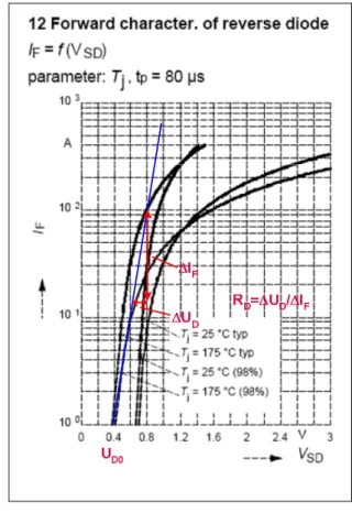
The conduction losses of the anti-parallel diode can be estimated using a diode approximation with a series connection of DC voltage source (uD0) representing diode on-state zero-current voltage and a diode on-state
resistance (RD), uD being the voltage across the diode and iF the current through the diode:
F D D D D
i
u
R
i
u
(
)
=
0+
⋅
These parameters can be read from the diagrams in the MOSFET datasheet as shown in fig. 2. In order to take the parameter variation into account, and thus to have a conservative calculation, the uD0 value read
from the diagram have to be scaled with (uDmax/uDtyp). Those exact values can be read from the datasheet
tables, but for an engineering calculation a typical safety margin value of (10%-20%) can also be used.
Figure 2 Diode resistance as a function of the diode current
The instantaneous value of the diode conduction losses is:
)
(
)
(
)
(
)
(
)
(
2 0i
t
R
i
t
u
t
i
t
u
t
p
CD=
D⋅
F=
D⋅
F+
D⋅
FIf the average diode current is IFav, and the rms diode current is IFrms, the average diode conduction losses
across the switching period (Tsw=1/fsw) are:
2 0 0 2 0 0
))
(
)
(
(
1
)
(
1
Frms D Fav D Tsw F D F D sw Tsw CD sw CDu
i
t
R
i
t
dt
u
I
R
I
T
dt
t
p
T
P
=
∫
=
∫
⋅
+
⋅
=
⋅
+
⋅
MOSFET Converter Losses
2.1.1
R
DSon- Taking the Temperature and Production Variations into Account
The procedure for RDSon determination, shown in figure 1, refers to the RDSon typical values. While this
procedure should be satisfying for the majority of applications, the RDSon value can be calculated by taking
into account the temperature and production variations. It can be done using following equation:
C T DSonMAX J DSon J
C
R
T
R
° −
+
⋅
=
25100
1
)
25
(
)
(
oα
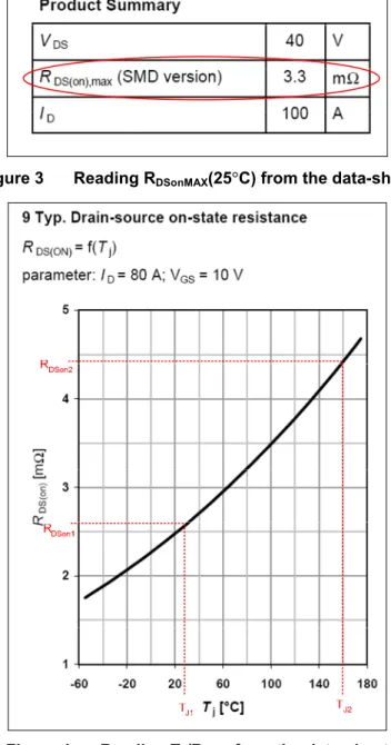
where TJ is the junction temperature and RDSonMAX(25°C) is the maximum value of RDSon at 25°C, which can
be read from the product summary table in the data-sheet as shown in the fig. 3. The temperature coefficient α can be calculated in the following manner: Two sets of values (TJ1, RDSon1) and (TJ2, RDSon2) can be read
from the data sheet as shown in fig. 4. These values can be used with the last equation to determine α.
Figure 3 Reading RDSonMAX(25°C) from the data-sheet
MOSFET Converter Losses
2.2 Switching
Losses
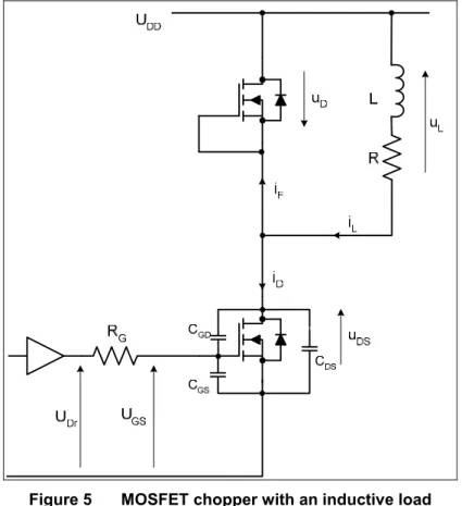
The circuit for the examination of the MOSFET switching losses is presented in fig. 5. It is a single-quadrant chopper supplying an inductive type load. The MOSFET is driven from the driver circuit, providing a voltage UDr at its output. The MOSFET internal diode is used as a free-wheeling diode, because in the majority of
applications, such as 3-phase AC motor drives, DC-motor drives, synchronous DC/DC converters, etc., the power electronics converter consists of one or more MOSFET-based half-bridges. If an external free-wheeling diode is used, the calculations are still valid, provided the diode parameters are taken from the diode data-sheet.
Figure 5 MOSFET chopper with an inductive load
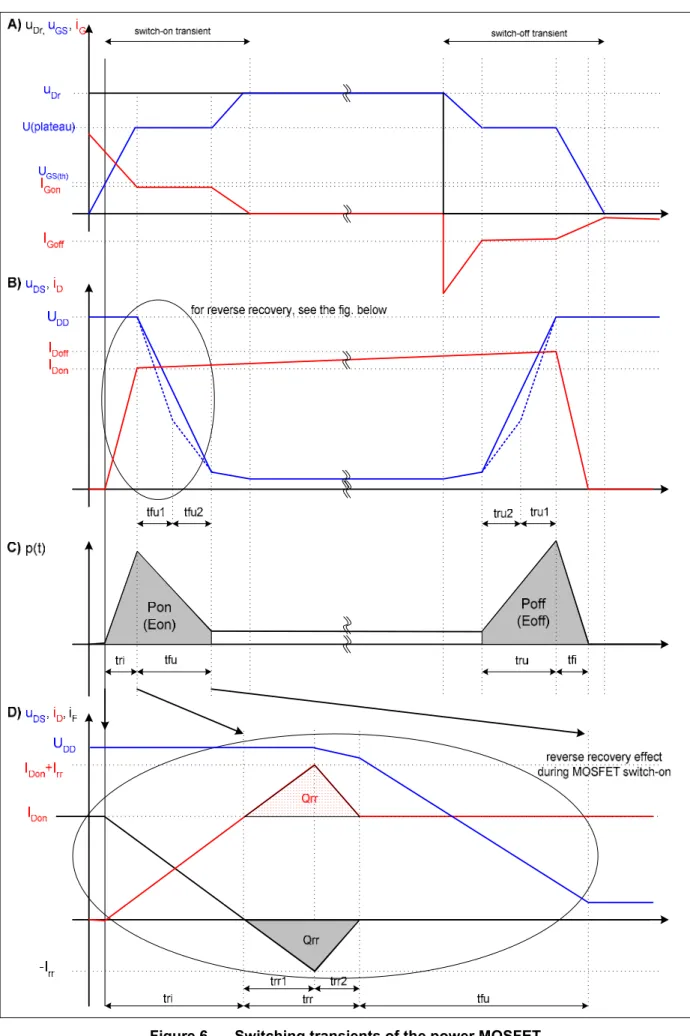
For the engineering calculations of the power loss balance, a linear approximation of the MOSFET switching process is sufficient and, as will be shown later, presents the worst case calculation. The idealised switching process of the power MOSFET is presented in Fig. 6. The uppermost part (A) presents the gate voltage (uGS)
and current (iG); the next one (B) shows the drain-source voltage (uDS) and the drain current (iD) without
taking the reverse recovery of the free-wheeling diode into account. The part C gives a qualitative overview of the power losses, while the part D shows the reverse-recovery effects on the switching losses.
2.2.1
Switch-on transient
• Driver circuit changes its state from 0V to UDr, the gate voltage rises to the threshold voltage (UGS(th)),
with the time-constant defined by the gate resistor and the equivalent MOSFET input capacitance (Ciss=CGD+CGS). Until the gate voltage reaches the UGS(th), the output does not change.
• After the UGS(th) has been reached, the drain current rises and takes over the load current. The worst
case value of the current rise-time (tri) between zero and IDon (defined by the application) can be
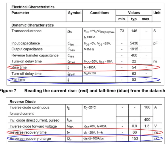
read from the MOSFET data-sheet, as shown in fig. 7. During the current rise-time, the free-wheeling diode is still conducting and the drain-source voltage is UDD.
• In order for the diode to switch off, all the minority carriers stored in it have to be removed (see fig. 6D). This reverse-recovery current has to be absorbed by the MOSFET, causing additional power losses. The worst-case values of the reverse-recovery charge (Qrr) and duration (trr), which will be used in the power loss calculation, can again be read from the MOSFET data-sheet (see fig. 8)
MOSFET Converter Losses
MOSFET Converter Losses
Figure 7 Reading the current rise- (red) and fall-time (blue) from the data-sheet
Figure 8 Reading the reverse recovery time (red) and charge (blue) from the data-sheet
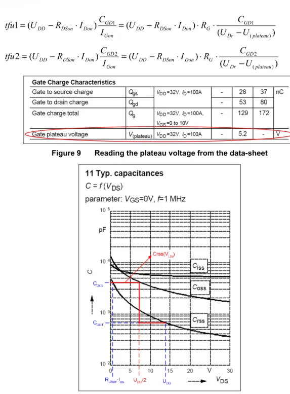
• After the diode has been switched off, the drain-source voltage is falling from uDS=UDD to its on-state
value uDS=RDSon·Ion. The Miller effect takes place and the gate-source voltage is clamped at the
uGS=U(plateau) (see fig. 9). The slope of the drain-source voltage is dictated through the gate current
flowing through the gate-drain capacitance (CGD=Crss). In order to calculate the voltage fall-time (tfu)
with a reasonable accuracy, the non-linearity of the gate-drain capacitance has to be taken into account. The typical dependence of the gate-drain capacitance on the drain-source voltage is shown in the fig. 10. Such non-linearity can not be easily incorporated into the engineering calculations. That is why a two-point approximation is used. It is supposed that if the drain-source voltage is in the range uDS∈[UDD/2,UDD], then the gate-drain capacitance takes value of CGD1= CGD(UDD). On the other
hand, if the drain-source voltage is in the range uDS∈[0V,UDD/2], then the gate-drain capacitance
takes value of CGD2= CGD(RDSon·Ion). The way to determine those capacitances is shown in fig. 10.
The drain-source voltage during the fall time, the two-point approximation being taken into account, is shown in fig. 6B with the dotted line. Since this approximation is used only to determine the voltage fall time (as well as the rise time during switch off) and the drain-source voltage is assumed to have the linear form (solid line in fig. 6B), it becomes clear that this analysis presents the worst-case for the switching losses calculation.
The gate current during tfu can be calculated as:
G plateau Dr Gon
R
U
U
I
=
−
( )The voltage fall time can now be calculated as a median of the fall times defined through the gate current and the capacitances CGD1 and CGD2.
2
2
1
tfu
tfu
tfu
=
+
where:MOSFET Converter Losses
)
(
)
(
)
(
1
) ( 1 1 plateau Dr GD G Don DSon DD Gon GD Don DSon DDU
U
C
R
I
R
U
I
C
I
R
U
tfu
−
⋅
⋅
⋅
−
=
⋅
−
=
)
(
)
(
)
(
2
) ( 2 2 plateau Dr GD G Don DSon DD Gon GD Don DSon DDU
U
C
R
I
R
U
I
C
I
R
U
tfu
−
⋅
⋅
⋅
−
=
⋅
−
=
Figure 9 Reading the plateau voltage from the data-sheet
Figure 10 Two-point representation of the gate-drain capacitance
2.2.2
Switch-off transient
Switch-off process corresponds to the switching-on process of the MOSFET in the reverse order and will thus not be discussed in detail. Two important differences are:
• No reverse recovery takes place
• The gate current and the voltage rise time can be expressed as:
G plateau Goff
R
U
I
=
−
( )MOSFET Converter Losses
2
2
1
tru
tru
tru
=
+
) ( 1 1(
)
)
(
1
plateau GD G Don DSon DD Goff GD Don DSon DDU
C
R
I
R
U
I
C
I
R
U
tru
=
−
⋅
=
−
⋅
⋅
⋅
) ( 2 2(
)
)
(
2
plateau GD G Don DSon DD Goff GD Don DSon DDU
C
R
I
R
U
I
C
I
R
U
tru
=
−
⋅
=
−
⋅
⋅
⋅
2.2.3
Switching Energies and Losses
According to previous considerations, the worst case turn-on energy losses in power MOSFET (EonM) can be
calculated as the sum of the switch-on energy without taking the reverse recovery process into account (EonMi) and the switch-on energy caused by the reverse-recovery of the free-wheeling diode (EonMrr):
DD rr Don DD onMrr onMi tfu tri D DS onM
Q
U
tfu
tri
I
U
E
E
dt
t
i
t
u
E
=
∫
⋅
=
+
=
⋅
⋅
+
+
⋅
+2
)
(
)
(
0The peak of the reverse-recovery current can be calculated as:
trr
Q
I
rr Frrpeak⋅
=
2
Turn-on energy in the diode consists mostly of the reverse-recovery energy (EonD):
Drr rr onDrr tfu tri F D onD
u
t
i
t
dt
E
Q
U
E
=
∫
⋅
≈
=
⋅
⋅
+4
1
)
(
)
(
0where UDrr is the voltage across the diode during reverse recovery. For the worst case calculation this
voltage can be approximated with a supply voltage (UDrr= UDD).
The switch-off energy losses in the MOSFET can be calculated in the similar manner. The switch-off losses in the diode are normally neglected (EoffD≈0). Therefore:
2
)
(
)
(
0tfi
tru
I
U
dt
t
i
t
u
E
DD Doff tfi tru D DS offM+
⋅
⋅
=
⋅
=
∫
+The switching losses in the MOSFET and the diode are the product of switching energies and the switching frequency (fsw): sw offM onM swM
E
E
f
P
=
(
+
)
⋅
sw onD sw offD onD swDE
E
f
E
f
P
=
(
+
)
⋅
≈
⋅
2.3 Loss
Balance
Power losses in the MOSFET and the free-wheeling diode can be expressed as the sum of the conduction and switching losses giving:
sw offM onM Drms DSon swM CM M
P
P
R
I
E
E
f
P
=
+
=
⋅
2+
(
+
)
⋅
sw onD Frms D Fav D swD CD DP
P
u
I
R
I
E
f
P
=
+
=
⋅
+
⋅
2+
⋅
0MOSFET Converter Losses
3 Application
Specific
Parameters
In the following text the typical applications will be revisited together with the typical signal waveforms necessary for the power loss balance calculation.
3.1
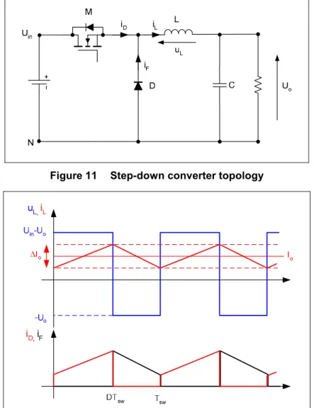
Step-down (Buck) Converter
Figures 11 and 12 present the topology and the typical signals in the step-down (buck) converter.
Figure 11 Step-down converter topology
Figure 12 Step-down converter – typical signals
Input parameters for the calculation: Input voltage (Uin), output voltage (Uo), output power (Po), inductor value
(L), switching frequency (fsw). Output current: o o o
U
P
I
=
Duty cycle in continuous conduction mode:
in o
U
U
D
=
MOSFET Converter Losses
sw o of
L
U
D
I
⋅
−
=
∆
(
1
)
The parameters needed for the loss calculation can be determined according to previously calculated values as:
2
o o DonI
I
I
=
−
∆
2
o o DoffI
I
I
=
+
∆
2 2 2(
)
o o DrmsD
I
D
I
I
=
⋅
=
⋅
o FavD
I
I
=
(
1
−
)
⋅
2 2 2(
1
)
(
1
)
o o FrmsD
I
D
I
I
=
−
⋅
=
−
⋅
3.2
Step-up (Boost) Converter
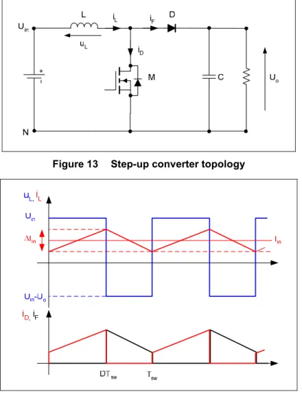
Figures 13 and 14 present the topology and the typical signals in the step-up (boost) converter.
Figure 13 Step-up converter topology
MOSFET Converter Losses
Input parameters for the calculation: Input voltage (Uin), output voltage (Uo), output power (Po), input power
(Pin), inductor value (L), switching frequency (fsw).
Input current: in in in
U
P
I
=
Duty cycle in continuous conduction mode:
o in
U
U
D
=
1
−
Input current ripple:
sw in in
f
L
U
D
I
⋅
⋅
=
∆
The parameters needed for the loss calculation can be determined according to previously calculated values as:
2
in in DonI
I
I
=
−
∆
2
in in DoffI
I
I
=
+
∆
2 2 2(
)
in in DrmsD
I
D
I
I
=
⋅
=
⋅
in FavD
I
I
=
(
1
−
)
⋅
2 2 2(
1
)
(
1
)
in in FrmsD
I
D
I
I
=
−
⋅
=
−
⋅
3.3
DC Motor Drive
Figures 15 and 16 present the topology and the typical signals in the single-quadrant chopper for the DC motor drive.
MOSFET Converter Losses
Figure 16 Single-quadrant DC motor drive – typical signals
Input parameters for the calculation: Input voltage (UDD), output voltage (Uo), output power (Po), armature
inductor value (L), armature resistance value (R), motor back-emf value (E), switching frequency (fsw).
Average value of the output current:
o o o
U
P
I
=
Duty cycle in continuous conduction mode:
DD o
U
U
D
=
Minimum output current:
R
E
e
e
R
U
I
R L fsw R L fsw D DD o−
−
−
=
⋅ 1 min1
1
Maximum output current:
R
E
e
e
R
U
I
R L fsw R L fsw D DD o−
−
−
=
− ⋅ − 1 max1
1
Output current ripple:
min max o o o
I
I
I
=
−
∆
The parameters needed for the loss calculation can be determined according to previously calculated values as:
2
o o DonI
I
I
=
−
∆
MOSFET Converter Losses
2
o o DoffI
I
I
=
+
∆
2 2 2(
)
o o DrmsD
I
D
I
I
=
⋅
=
⋅
o FavD
I
I
=
(
1
−
)
⋅
2 2 2(
1
)
(
1
)
o o FrmsD
I
D
I
I
=
−
⋅
=
−
⋅
Figures 17…18 present the topology and the typical signals in the four-quadrant chopper for the DC motor drive. Fig. 18 shows the case of the bipolar PWM, while the fig. 19 shows the case of the unipolar PWM. Appropriate values can be determined following the same procedure as for the single-quadrant chopper, taking into account that for the bipolar PWM the voltage excursion on the load is 2UDD.
Figure 17 Four-quadrant DC motor drive
MOSFET Converter Losses
Figure 19 Four-quadrant DC motor drive – typical signals with unipolar PWM
3.4
Three-Phase AC Motor Drive
Figures 19 and 20 present the topology and the typical signals in the three-phase inverter for the AC motor (permanent magnet synchronous, brushless DC, induction motor) drive. Typical applications are: electric power steering (EPS), Starter-Generator (Alternator), fans, blowers, HVAC etc.
Figure 20 Three-phase AC motor drive
Input parameters for the calculation: Input voltage (UDD), output line-to-line voltage (Uo) or output phase
voltage (Uan1), rms value of the output current (Iorms) or output apparent power (So=3Uan1Iorms), motor
displacement factor (cosφ1), equivalent stator inductance (L), switching frequency (fsw), output (motor
electrical) frequency fo and an inverter amplitude modulation index ma
Output current ripple:
sw DD o o DD a
L
U
f
U
U
U
I
⋅
⋅
⋅
⋅
⋅
−
=
∆
2
)
2
(
Peak value of the output current:
orms o
I
MOSFET Converter Losses
MOSFET conduction losses:
)
3
1
cos
8
1
(
2 2π
φ
⋅
⋅
+
⋅
⋅
=
⋅
=
a o DSon Drms DSon CMm
I
R
I
R
P
Diode Conduction losses:
)
3
1
cos
8
1
(
)
8
1
cos
2
1
(
2 0 2 0π
φ
φ
π
⋅
⋅
−
⋅
⋅
+
⋅
−
⋅
⋅
⋅
=
⋅
+
⋅
=
a o D a o D Frms D Fav D CDm
I
R
m
I
u
I
R
I
u
P
In order to find a simple solution for the switching loss calculation, it is supposed that the losses generated in the inverter in one half-wave of the output frequency (1/(2 fo) ) correspond to the losses generated if instead
of AC output current a DC equivalent output current is applied. The equivalent DC output current value is:
o DC
I
I
=
⋅
π
1
This value can be used for [IDon, IDoff] in the switching loss calculation as described in detail in the chapter 2.3.
MOSFET Converter Losses
3.5
Switched Reluctance Motor Drive
Figures 22, 23 and 24 present the topology and the typical signals in the two-quadrant chopper for one phase of the switched reluctance motor drive. The complete converter consists of more two-quadrant converters, the number of which depends on the number of the motor phases. The procedure for the power loss calculation is practically the same as with the DC motor drive and therefore the same equations can be used.
Figure 22 Two-quadrant converter for one phase winding of the switched reluctance motor drive
MOSFET Converter Losses
Figure 24 Switched reluctance motor drive – typical signals with unipolar PWM
3.6 Piezo-Electric
Actuator
Figures 25 and 26 present the topology and the typical signals in the two-quadrant DC/DC converter for the piezo-electric actuator, used, for example, in direct injection systems. The procedure for the power loss calculation is the same as with the step-down (buck) converter during charging and the same as with the step-up (boost) converter during the discharging. Namely, while the actuator is charging, the system behaves like a step-down converter (MOSFET 1 and Diode 2 are active) and the energy flows from UDD to CA and the
energy flow reverses while the CA is discharging (MOSFET 2 and Diode 1 are active).
MOSFET Converter Losses
Figure 26 Converter for piezo-electric actuator – typical signals
4 Conclusion
This Application Note presented a mathematical tool for the calculation of power losses in MOSFET-based power electronics converters used in automotive applications. Mathematical model for the power loss balance calculation using the data-sheet parameters was presented. The typical automotive applications were reviewed and the application specific parameters important for the loss balance were extracted.
MOSFET Converter Losses
5 Abbreviations
Pl Power losses
Pc Conduction losses
Psw Switching losses
Pb Blocking (leakage) losses
pCM Instantaneous value of the MOSFET conduction losses
PCM Average value of the MOSFET conduction losses
pCD Instantaneous value of the diode conduction losses
PCM Average value of the diode conduction losses
PswM MOSFET switching losses
PswD Diode switching losses
PM MOSFET losses
PD Diode losses
Po Converter output power
EonM MOSFET switch-on energy
EonMi MOSFET switch-on energy without taking the reverse recovery process into account
EonMrr MOSFET switch-on energy caused by the reverse-recovery of the free-wheeling diode
EonD Diode energy during MOSFET switch-on transient
EoffM MOSFET switch-off energy
uDS Drain-source voltage
uD Voltage across the diode
uD0 Diode on-state zero-current voltage
UDr Driver output voltage
UGS Gate-source voltage
UGSth Gate-source threshold voltage
U(plateau) Plateau voltage
UDrr Voltage across the diode during reverse recovery
UDD Converter supply (DC bus) voltage
Uin Converter input voltage
Uo Converter output voltage
uL Voltage across the load
iD Drain current
IDrms RMS value of the drain current
iF Current through the diode
IFav Average diode current
IFrms RMS value of the diode current
Irr Reverse recovery current
MOSFET Converter Losses
IG Gate current
iL Load current
Iin Converter input current
Io Converter output current
RDSon Drain source on-state resistance
RD Diode on-state resistance
RG Gate resistor
CGS Gate-source capacitance
CGD Gate-drain capacitance
CDS Drain-source capacitance
Qrr Reverse recovery charge R Load resistor L Load Inductance Tj Junction temperature α Temperature coefficient Tsw Switching period fsw Switching frequency
tri Current rise time tfi Current fall time tru Voltage rise time tfu Voltage fall time trr Reverse recovery time D Duty cycle
Edition 2006-07-31
Published by Infineon Technologies AG, Am Campeon 1-12,
85579 Neubiberg, Germany
© Infineon Technologies AG 2006. All Rights Reserved.
LEGAL DISCLAIMER
THE INFORMATION GIVEN IN THIS APPLICATION NOTE IS GIVEN AS A HINT FOR THE
IMPLEMENTATION OF THE INFINEON TECHNOLOGIES COMPONENT ONLY AND SHALL NOT BE REGARDED AS ANY DESCRIPTION OR WARRANTY OF A CERTAIN FUNCTIONALITY, CONDITION OR QUALITY OF THE INFINEON TECHNOLOGIES COMPONENT. THE RECIPIENT OF THIS APPLICATION NOTE MUST VERIFY ANY FUNCTION DESCRIBED HEREIN IN THE REAL APPLICATION. INFINEON TECHNOLOGIES HEREBY DISCLAIMS ANY AND ALL WARRANTIES AND LIABILITIES OF ANY KIND (INCLUDING WITHOUT LIMITATION WARRANTIES OF NON-INFRINGEMENT OF INTELLECTUAL PROPERTY RIGHTS OF ANY THIRD PARTY) WITH RESPECT TO ANY AND ALL INFORMATION GIVEN IN THIS APPLICATION NOTE.
Information
For further information on technology, delivery terms and conditions and prices please contact your nearest Infineon Technologies Office (www.infineon.com).
Warnings
Due to technical requirements components may contain dangerous substances. For information on the types in question please contact your nearest Infineon Technologies Office.
Infineon Technologies Components may only be used in life-support devices or systems with the express written approval of Infineon Technologies, if a failure of such components can reasonably be expected to cause the failure of that life-support device or system, or to affect the safety or effectiveness of that device or system. Life support devices or systems are intended to be implanted in the human body, or to support