ISSN:
2231-5381
http://www.ijettjournal.org
Page 97Voltage Balancing in Diode Clamped Multilevel
Inverter Using Sinusoidal PWM
S.Shalini (1)
Assistant Professor, Department of Electrical and electronics engineering Roever Engineering College, Perambalur, Anna university,Tamilnadu,India
Abstract— Multilevel inverters offer several advantages compared to the conventional 3-phase bridge inverter in terms of lower dv/dt stresses, lower electromagnetic compatibility, smaller rating and better output features. This project presents a 9-level diode Clamped inverter using Sinusoidal pulse width Modulation techniques as the control strategies. The algorithm has been developed within the carrier-based PWM framework to facilitate its implementation in diode clamped converters with three or more levels. A simulation model of 9-level DCMI has been designed and developed. The results obtained from the simulation model have been compared with the 3-level and 5-level diode clamped inverter. By increasing the level of inverter, effective balancing in line voltage and reduced THD is obtained.The good performance of the proposed modulation technique is demonstrated from simulation results for a nine-level diode-clamped inverter and the 3-level diode clamped inverter hardware model is designed and exhibited.
Keywords— SPWM, THD, DCMI
I. INTRODUCTION
Multilevel inverter is based on the fact that sine wave can be approximated to a stepped waveform having large number of steps. The steps being supplied from different DC levels supported by series connected batteries or capacitors. The unique structure of multi- level inverter allows them to reach high voltages and therefore lower voltage rating device can be used. As the number of levels increases, the synthesized output waveform has more steps, producing a very fine stair case wave and approaching very closely to the desired sine wave. It can be easily understood that as motor steps are included in the waveform the harmonic distortion of the output wave decrease, approaching zero as the number of levels approaches infinity. Hence Multi-level inverters offer a better choice at the high power end because the high volt- ampere ratings are possible with these inverters without the problems of high dv/dt and the other associated ones.
II. MULTILEVEL INVERTER TOPOLOGIES
The basic three types of multilevel topologies used are
(1) Diode clamped multilevel inverters (2) Flying capacitors multilevel inverter or Capacitor clamped multilevel inverter (3) Cascaded inverter with separate dc source
A. DIODE CLAMPED MULTILEVEL INVERTER
The first invention in multilevel converters was the so-called neutral point clamped inverter. It was initially proposed as a three level inverter. It has been shown that the principle of diode clamping can extended to any level. A diode clamped leg circuit is shown in Figure.
The main advantages and disadvantages of this topology are:
Advantages:
• High efficiency for the fundamental switching frequency.
• The capacitors can be pre-charged together at the desired voltage level.
• The capacitance requirement of the inverter is minimized due to all phases sharing a common DC link.
Disadvantages:
• Packaging for inverters with a high number of levels could be a problem due to the quadratically relation between the number of diodes and the numbers of levels.
• Intermediate DC levels tend to be uneven without the appropriate control making the real power transmission a problem.
ISSN:
2231-5381
http://www.ijettjournal.org
Page 98Fig.1 5-level structure of DCMI
Some of the applications using Multilevel Diode Clamped converters are:
• An interface between High voltage DC transmission line and AC transmission line.
• High power medium voltage variable speed drives. • Static VAR compensation
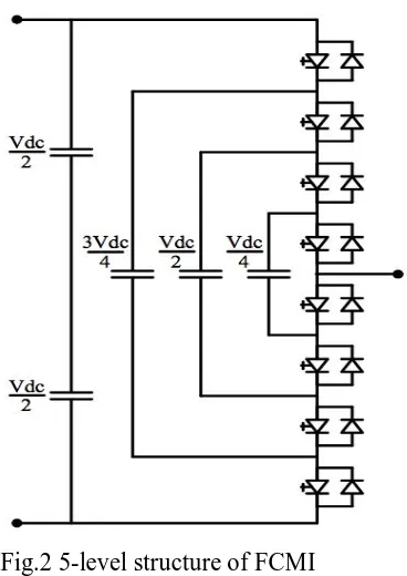
B.FLYING-CAPACITORMULTILEVEL INVERTER
As an alternative for the diode clamped inverter is the capacitor clamped inverter proposed by Meynard and Foch, which shared many of the advantages. The structure of the capacitor clamped inverter is similar to that of the diode clamped converter. The main difference is that the diodes used for the clamping are replaced by capacitors. A Flying capacitor Converter leg circuit is shown in Figure. For this topology the most common application is static VAR generation.
Fig.2 5-level structure of FCMI
C.CASCADED MULTILEVEL INVERTER
The cascaded multilevel inverter is based on the series connection of single leg or double leg (H bridges) inverters with separate DC sources or capacitors. For each of these two types of configurations several states exist regarding to the switches states. Figure , the single leg unit, has 2 states for each of the two possible current(s) directions while the double unit has 4 states.
ISSN:
2231-5381
http://www.ijettjournal.org
Page 99Fig 3.Single leg unit and Double leg unit connection
III PULSE WIDTH MODULATION
Pulse Width Modulation refers to a method of carrying information on a train of pulses, the information being encoded in the width of the pulses. The pulses have constant amplitude but their duration varies in direct proportion to the amplitude of analog signal. PWM is the most popular method for producing a controlled output for inverters. They are quite popular in industrial applications. The modulation techniques used for high switching frequency PWM are
Space vector modulation(SVM)
Sinusoidal PWM
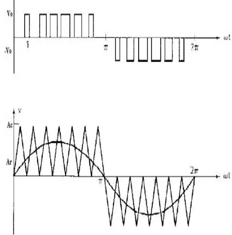
SINUSOIDAL PWM
In this modulation technique there are multiple numbers of output pulses per half cycle and pulses are of different width. The width of each pulse is varying in proportion to the amplitude of a sine wave evaluated at the centre of the same pulse. Carrier Based Pulse width modulation (CBPWM) or SPWM technique has been extensively used, because it improves the harmonic spectrum of the
inverter by moving the voltage harmonic
components to higher frequencies The gating signals are generated by comparing a sinusoidal reference with a high frequency triangular signal.
Fig 4.Sinusoidal pulse width modulation
IV. SIMULATION RESULT
Simulation of various inverters using sinusoidal pulse width modulation was carried out with the help of “MATLAB 7.8”.Simulation was carried out to observe the improvement in the line voltage THD and as the inverter level increases from 3-level to 5-level. Following quantities have been served.
1. Line voltage wave form for 3-level and 5- level is obtained
2. Line to Line voltage wave form is obtained for 3-level and 5- level.
3. Line to Neutral waveform is obtained for 3- level and 5- level.
ISSN:
2231-5381
http://www.ijettjournal.org
Page 100V. 3-LEVEL DCMI
Fig.4 Simulation circuit
Fig.5 Pulse generation
Fig.6 Line to line voltage waveform
Fig.7 Line to neutral voltage waveform
Fig.8 Line voltage waveform
VI . 5-LEVEL DCMI
ISSN:
2231-5381
http://www.ijettjournal.org
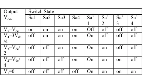
Page 101TABLE-I
5-Level DCMI voltage levels & their switching states
Fig. 9 Simulation circuit (5-level DCMI)
Fig.10 Pulse generation circuit
Fig .11 Pulse distribution circuit
Fig.12 Line to line voltage waveform
Fig.13 Line to neutral voltage waveform
Fig.14 Line voltage waveform Output
VAO
Switch State
Sa1 Sa2 Sa3 Sa4 Sa’ 1
Sa’ 2
Sa’ 3
Sa’ 4 V5=Vdc on on on on Off off off off
V4=3Vdc
/4
off on on on On off off off
V3=Vdc/
2
off off on on On on off off
V2=Vdc/
4
off off off on On on on off
ISSN:
2231-5381
http://www.ijettjournal.org
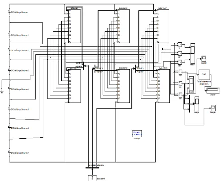
Page 102VII. 9-LEVEL DCMI
A three-phase nine-level diode-clamped inverter is shown in fig.4. Each phase is constituted by 16 switches (eight switches for upper leg and eight switches for lower leg). Switches Sa1 through Sa8 of upper leg form complementary pair with the switches Sa1’ to Sa8’ lower leg of the same phase. The complementary switch pairs for phase ‘A’ are
(Sa1, Sa1’), (Sa2, Sa2’),(Sa3, Sa3’),(Sa4,
Sa4’),(Sa5, Sa5’),(Sa6, Sa6’),(Sa7, Sa7’),(Sa8, Sa8’) and similarly for B and C phases. Clamping diodes are used to carry the full load current
Fig. 15 Circuit Diagram of 3 Phase Nine Level Diode Clamped Inverter
TABLE-II
Pole Voltage and Line Voltage of a Nine Level Inverter
Fig. 16 Simulation circuit
Fig.17 Simulation circuit
Sa1 Sa2 Sa3 Sa4 Sa5 Sa6 Sa7 Sa8 VAB VAO
1 1 1 1 1 1 1 1 Vdc Vdc
0 1 1 1 1 1 1 1 Vdc/8 3Vdc/4
0 0 1 1 1 1 1 1 2Vdc/8 2Vdc/4
0 0 0 1 1 1 1 1 3Vdc/8 Vdc/4
0 0 0 0 1 1 1 1 4Vdc/8 0
0 0 0 0 0 1 1 1 5Vdc/8 -Vdc/4
0 0 0 0 0 0 1 1 6Vdc/8 -2Vdc/4
0 0 0 0 0 0 0 1 7Vdc/8 -3Vdc/4
ISSN:
2231-5381
http://www.ijettjournal.org
Page 103Fig 18 Line to Line voltage waveform
TABLE-III
Comparison of THD Level
Diode Clamped Multilevel
Inverter THD%
3-Level 47.42%
5-Level 31.52%
9-Level 19.51%
REFERENCES
[1] J. S. Lai and F.Z. Peng “Multilevel Converters – A new breed of power converters” IEEE Trans. Ind Applicant , Vol. 32, May/June 1996. [2] Jose Roderiguez, Jih-Sheng Lai and Fang Zheng Reng, “Multilevel
Inverters” A survey of topologies ,control, and applications “,IEEE Trans. On Ind.Electronics, vol No.[4], August 2002.
[3] A. Nabae, I Takashashi, and H. Akagi, “ A new neutral –point clamped PWM inverter,” IEEE Trans. Ind Application Vol. No. IA-17,PP 518-523,Sept/oc 1981.
[4] P.K.Chaturvedi, S. Jain, Pramod Agrawal “ Modeling , Simulation and Analysis of Three level Neutral Point CLAMPED inverter using matlab/Simulink/Power System Blockst”
[5] Bor-Ren Lin & Hsin – Hung Lu “ A Novel Multilevel PWM Control Scheme of the AC/DC/AC converter for AC Drives”IEEE Trans on ISIE, 1999.
[6] B. R. Lin & H- H Lu “ multilevel AC/DC/AC Converter for AC Drives” IEEE Proceding electronics Power application, Vol 146, No. 4, July 1999.
[7] DAI Bin “ A new control scheme for voltage Source Inverter Without DC Link Capacitor Under Abnormal Input Voltage Conditions” IEEE Tran.2009.
[8] K. Arab tehrani, H. Andriasioharana, I. Rasonarivo & F.M. Sargos “ A Multilevel Inverter Model” IEEE Trans. 2008.
[9] Siriroj Sirisukprasert, Jih- Sheng Lai & Tina – Hua Liu “Optimum harmonics Reduction With A wide Range Of Modulation Indexes for Multilevel Converters” IEEE Trans Ind Application Electronics ,Vol 49 , No. 4, August 2002.
[10] G.Bhuvaneshwari and Nagaraju “ Multilevel inverters – a comparative study” vol .51 No.2 march – april 2005. [11] Siriroj Sirisukprasert “ Optimum harmonics reduction”.
[12] A. M. Massoud, S.J. Finney and B.W. Williams “Control Techniques for Multilevel Voltage Source Inverters” IEEE proce. 2003.
[13] B.R. Lin and H.H. Lu “ Multilevel AC/DC/AC converter for AC drives” IEE E Proc.—Electr. Power Application, Vol. 146, No. 4, July 1999. [14] M. A. EL- Barky, S.H. Arafah “ Simulation and Implemetaion of Three
Phase Three Level Inverter” SICE july 25- 27, 2001, Nagoya.