A 16-Bit Fully Functional Single Cycle
Processor
Nidhi Maheshwari (Student)
Electronics & Instrumentation Engg. Department,
Shri G.S.Institute of Technology and Science,
Indore, India
Mobile no.:-+919039969095
Pramod Kumar Jain (Asso. Professor)
Electronics & Instrumentation Engg. Department,
Shri G.S.Institute of Technology and Science,
Indore, India
Mobile no.:-+918878122571
D.S. Ajnar (Asso. Professor)
Electronics & Instrumentation Engg. Department,
Shri G.S.Institute of Technology and Science,
Indore, India
Mobile no.:-+919406681443
Abstract:-The existing commercial microprocessors are provided as black box units, with which users are
unable to monitor internal signals and operation process, neither can they modify the original structure. In
order to solve this problem 16-bit fully functional single cycle processor is designed in terms of its
architecture and its functional capabilities. The procedure of design and verification for a 16-bit processor
is introduced in this paper. The key architecture elements are being described, as well as the hardware
block diagram and internal structure. The summary of instruction set is presented. This processor is
modify as a Very High Speed Integrated Circuit Hardware Description Language (VHDL) and gives
access to every internal signal. In order to consume fewer resources, the design of arithmetic logical unit
(ALU) is optimized. The RTL views and verified simulation results of processor are shown in this paper.
Integrated Circuit Hardware Description Language (VHDL) code using Xilinx ISE 9.2i tool for synthesis
and simulation.
Keywords:-Arithmetic logical unit (ALU), control unit (CU), comparator, shifter, rotations, instruction set,
VHDL, Xilinx.
I. INTRODUCTION
Processors are divided into 3 categories:- 8-bit, 16-bit and 32-bit processor, depending upon the demand of
performance, cost, power and programmability. 8-bit processors have extreme low cost and consume less power
for simple control system. In contrast to 8-bit, 32-bit processors have high programmability, high performance
and are widely used in cellular phone and PDA that need high computation but it has high power consumption.
On the other hand 16-bit processors have high performance and power than 8-bit processor and low power
consumption than 32-bit processor. They are often used in 16-bit applications such as disk driver controller,
cellular communication and airbags.
The 16-bit fully functional single cycle processor is applicable for real tasks and also used for assembly language
programming. We need to participate in the process of processor design and to understand the inner structure of
processor. Therefore its architecture is well structured and simple enough so that it can be built by first grade
students, without any design experience. These all requirements can be obtained by the FPGA based processor
with Hardware Description Language VHDL. Figure 1 shows the basic steps to design the processor.
The remaining paper is organized as follows. The next section of the paper describes the internal architecture of
16-bit fully functional single cycle processor, System operation and interaction between different units, ALU and
Instructions. Section III introduces functional simulation results. Section IV describes logic synthesis.
Figure 1:-Design Flow Steps Methodology
II. GENERAL ARCHITECTURE OF TEACHING PROCESSOR
A processor incorporates most or all of the functions of a computer’s Central Processing Unit (CPU) on a single
IC or microchip. In order to accomplish these several innovative and unconventional design trade offs have been
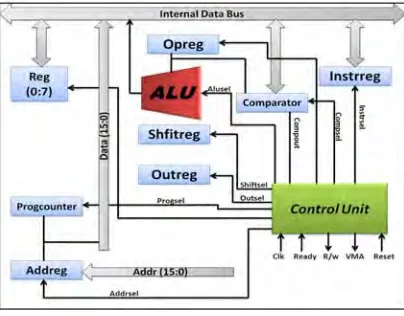
made, without compromising the goals. The general architecture of 16-bit teaching processor is shown in figure
2. It contains number of basic pieces. There is a register array of 8-bit and 16-bit, a 16-bit ALU, a 16-bit shifter,
a program counter, an instruction register, a 16-bit comparator, an address register and control unit. All of these
A. System Operations And Interaction Between Different Units:-
The top level design consists of the processor block and a memory block communicating through a
bi-directional data bus, an address bus, and few control lines. The processor fetches instructions from external
memory and executes these instructions to run a program. These instructions are stored in instruction register
and decoded by control unit. The control unit causes the appropriate signal interaction for processor unit to
execute the instruction.
If the instruction is an add of two registers, the control unit would cause the first register value to be written in
operational register (OpReg) for temporary storage. The second register value would then be placed on data bus.
The ALU is now set at add mode and result will be stored in output register (OutReg). Output register stores the
resulting value until it is copied to the final destination. When executing an instruction, number of steps takes
place. Program counter holds the address in memory of the current instruction. After an instruction has
finished execution, the program counter is advanced to where the next instruction is located. If the
processor is executing a linear stream of instructions, this is the next instruction. If a branch is taken, the
program counter is loaded with next instruction location directly. The processor values the address register,
which gives output as new address on the address bus. At the same time, control unit sets the R/W (read write
signals) to ‘0’ for read operation and sets signal VMA (Valid Memory Address) to ‘1’, signaling the
memory that the address is now valid. Memory decodes the address and places the memory data on data bus.
When data has been placed on data bus, memory set the READY signal to ‘1’ indicating that the memory data is
ready for consumption.
Control unit causes the memory data to be written into the instruction register. The control unit is now access
and decodes the instruction. The decoded instruction executes, and process starts over again.
Figure 2:- Internal architecture of 16-bit processor
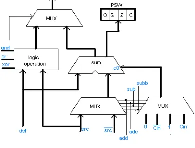
B. Arithmetic Logical Unit (ALU):-
The arithmetic operations are comprised of addition, addition with carry, subtraction, subtraction with borrow.
Most of the time behavioral method of hardware description is employed using the following expressions:
A+B
A+B+C
A-B
The behavioral capabilities of HDL can be more powerful and more convenient for some designs. However, in
this case the behavioral description will likely imply more adder unit usage in order to realize these functions.
The block diagram of the ALU is shown in Figure 3. It consumes only one adder unit and can co-operate with
the multiplexer to realize different calculations. Table 1 shows consumed resources of the two methods.
Figure 3:- ALU Block Diagram
Table 1:- Consumed Resources Report
Behavior
Description
Structural
Description
Number of Slices 54 49
Number of 4 input LUTs 80 77
An alternative way adopted, structural description is to split the ALU into two modules, Logic module and
Arithmetic module. During a component design experiment, to facilitate the manual operation, the parameter is
set as 4 bits; otherwise, for a principal machine design, only the parameter needs to be changed to 16 bits to
become a 16-bit ALU.
The advanced ALU has basic arithmetic and logical operations including addition (+), subtraction (-),
multiplication (*), negation (^), and in addition of some other operations such as bit shifts (<<,>>), bitwise logic
operations (&,/,^,~), and logical operations (&&,! ). ,װ
C. Instructions:-
Instructions can be divided into five major categories:-
CPU Control – instructions like NOP, STOP or SET do not generate numeric result but alter the
processor’s state. The SET and CLR instructions allow setting and clearing of any status or control
flag.
Data Transfer – instructions like MOV, LOAD or PUSH copy the content of an internal register to
another register, a memory location, or load the data from these sources to register file.
Branch and Subroutine -- instructions like JMP, CALL or RET alter the value of program counter
and access the call stack.
Arithmetic and Logic -- instructions like ADD, NEG or XOR generate numeric result as a function of
Multiplication and Division -- these instructions generate two results during execution. The
multiplication will output a 32-bit result and the division will output a quotient and a remainder.
Table 2:- Instruction Table
INSRUCTIONS TYPE NOTE
NOP No operation
SET Set operation
CLR Clear operation
JMP Jump operation
CALL Call operation
LOAD Load register
STORE Store register
MOVE Move value to register
LOADI Load register with immediate
value
BRANCHI Branch to immediate address
INC Increment
DEC Decrement
AND AND two register
OR OR two register
XOR XOR two register
NOT NOT a register
ADD Add two register
SUB Subtract two register
ZERO Zero a register
SHL Shift left
SHR Shift right
ROTR Rotate right
ROTL Rotate left
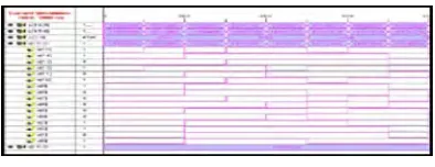
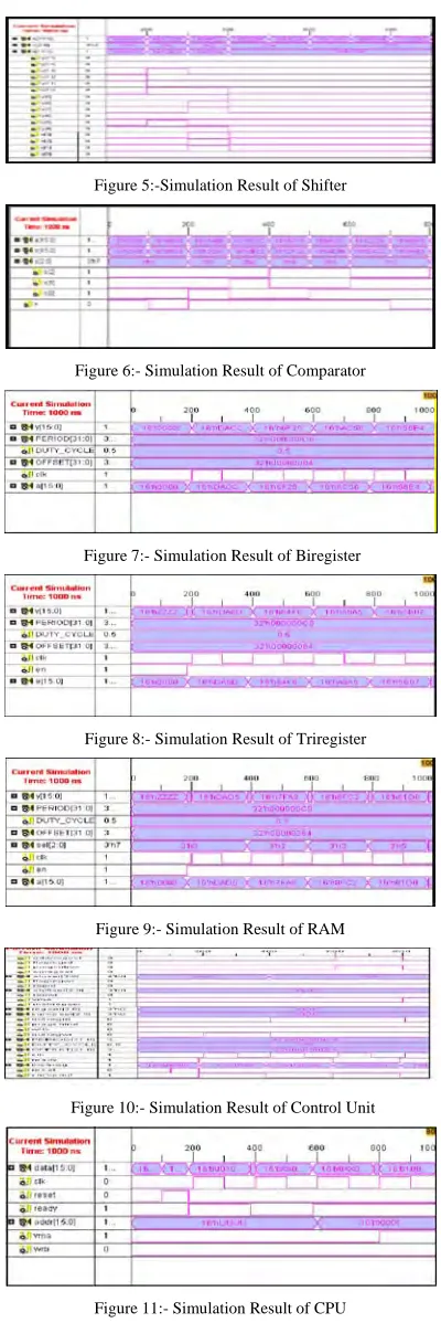
III.FUNCTIONAL SIMULATION RESULTS
Functional simulation is the way to verify a design. In our design we verify the components of processor by the
functional simulation and obtained the simulated data which confirms the work ability of our design. Here we also
found that functional simulation is also verified for the whole processor.
Figure 5:-Simulation Result of Shifter
Figure 6:- Simulation Result of Comparator
Figure 7:- Simulation Result of Biregister
Figure 8:- Simulation Result of Triregister
Figure 9:- Simulation Result of RAM
Figure 10:- Simulation Result of Control Unit
Figure 11:- Simulation Result of CPU
IV. LOGIC SYNTHESIS
The RTL description of a design is taken through logic synthesis in an EDA tool, which generates a gate-level
Figure 12:-RTL View of ALU
Figure 13:-RTL View of Shifter
Figure 14:-RTL View of Comparator
Figure 15:-RTL View of RAM
Figure 16:-RTL View of Control Unit
Figure 17:-RTL View of CPU
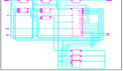
If we push the top-level design we can find the internal structure like this.
Figure 18:-Internal Structure of the CPU
V. CONCLUSION
The 16-bit fully functional single cycle processor was described using VHDL. The design of ALU was
advantage because it is an open core which benefits with an in-depth understanding of the microprocessor’s
interior structure. Functional simulation shows that the processor executes for all the various instructions. We
verified all the result and found them too correctly.
VI. REFERENCES
1. Andrei-Sorin F., Corneliu B., 2010 “Savage 16-16 bit RISC Architecture General Purpose Microprocessor” in Proc. IEEE Journal. (Pp.3-8)
2. Venelin Angelov, Volker L., 2009 “The Educational Processor Sweet-16” in Proc. IEEE Conference. (Pp.555-559)
3. Xiao Tiejun, Liu Fang, 2008 “16-bit Teaching Microprocessor Design and Application” in Proc. IEEE International Symposium on It in Medicine and Education. (Pp.160-163)
4. J. O. Hamblen and M. D. Furman, Rapid Prototyping of Digital Systems. Springer, 2001.
5. Cross, J.E. and Soetan, R. A., 1988 “Teaching Microprocessor Design using the 8086 Microprocessor” in Proc. IEEE Conference on Southeastcon’88. (Pp. 175-180)
6. D. L. Perry, VHDL, 3rd ed. McGraw-Hill, 1988.
7. J. Reichardt and B. Schwarz, VHDL-Synthesis. Oldenburg, 2001.