Design and Analysis of Parallel-Coupled
Line Bandpass Filter
Talib Mahmood Ali
Asst. Lecturer, Electrical Engineering Department, University of Mustansiriyah, Baghdad, Iraq
Abstract A compact microwave parallel coupled line resonator seventh order bandpass filter (BPF) is presented in this paper, consist a 8-parallel coupled line pairs designed for a maximally flat response or Butterworth response at a center frequency of 2.44175 GHz and with a fractional bandwidth, ∆= 0.035. The filter was implemented in a microstrip platform with a permittivity of the substrate Er=4.4 and a substrate height h=1.5mm. The physical parameters of the parallel coupled line filter sections were optimized using the Microwave Office software to provide the closest values of the bandpass filter prototype values and electrical lengths for a given set of filter specifications. The simulation of direct calculation, show the attenuation S11 response was observed at 2.44175 GHz with a value of 25 dB and the corresponding Insertion Loss S21 is -1.8dB while the optimized design S11 response at the centre frequency with a value of -113 dB and the corresponding Insertion Loss S21 is -2.2dB.
Keywords Parallel Coupled line Microstrip, Butterworth, microwave BPF. 1. Introduction
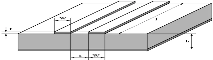
Microwave filters are two-port networks used in an electronic system capable of allowing transmission of signals over the pass-band and rejecting unwanted harmonics over the stop-band. Different kinds of approximations, like Butterworth, Chebyshev and Elliptic function [1] have been proposed and widely used as models for microwave-filter synthesis [2]. Butterworth Filters have the flattest possible pass-band magnitude response. That means all the derivatives of the amplitude with frequency are zero at DC [3]. The Butterworth response is a good compromise between attenuation characteristic and group delay. The group delay of Butterworth filters is reasonably flat but has a rise near the cut off frequency. The step response of these filters exhibits some ringing, which degrades its use for data communications.Parallel-coupled microstrip bandpass filters have been extensively adopted in the RF front end of microwave and wireless communication systems for decades. Two shortcomings limit the range of practical applications of coupled-line filters [4],[5]. The parallel coupled lines filter based on the odd and even wave coupling of transmission lines through a common ground plane, which results in odd and even characteristic line impedances. This sets the stage to an understanding of the coupling between two strip lines and their input/output impedances as part of a two port chain matrix representation. Cascading these elements gives rise to bandpass filter structures A simple modelling approach of coupled microstrip line interaction is established when considering the geometry depicted in Fig. 1. The parallel-coupled microstrip transmission lines can be used to construct many types of filters. The general conventional BPF structure of the parallel-coupled-line filter is based on the half-wavelength resonators [6],[7].
Figure 1. The parallel coupled lines microstrip geometry and structure.
2. Design procedure of the BPF
The design parameters of the proposed maximally flat BPF are; filter type: Butterworth, mean frequency fo = 2.44175 GHz, lower limiting frequency fmin=2.4 GHz upper limiting frequency fmax=2.4835 GHz, degree of filtration N = 7 and system impedance Zo = 50 Ω.
The degree of filtration, N, should always be selected to be odd (i.e.,3, 5, 7...), because the source resistance and the load resistance is identical under these conditions. The number of coupled line pairs is always 1 more than the selected degree of filtration. For N=7, there must thus be eight line pairs.
g2=1.2470 g6=1.2470 g3=1.8019 g5=1.8019 g4=2.000
Step 2 Calculating the fractional bandwidth of pass band:
∆ 2.4835 2.4
2.44175 ∆ 0.0341967
Step 3 The proposed filter involved eight line pairs admittance inverter constants for the eight line pairs, the admittance inverter constants was computed for all line pairs;
1. Determining the admittance inverter constants for 1st line pair:
∆
2 0.347434
2. Determining the admittance inverter constants for 2nd line pair:
∆
2 0.072109494
3. Determining the admittance inverter constants for 3th line pair:
∆
2 0.035834
4. Determining the admittance inverter constants for 4th line pair:
∆
2 0.2829598
5. Determining the admittance inverter constants for 5th line pair:
∆
2 0.0282959845
6. Determining the admittance inverter constants for 6th line pair:
∆
2 0.035834932
7. Determining the admittance inverter constants for 7th line pair:
∆
0.0721094069
8. Determining the admittance inverter constants for 8th line pair:
∆
2 0.34743420
Step 4: The EVEN and ODD impedances of line pairs was determined by following formulae
50Ω 1
50Ω 1
For 1st line pairs:
50Ω 1 0.347434 0.347434 73.407236Ω
50Ω 1 0.347434 0.347434 26.5927638Ω
For 2nd line pairs:
50Ω 1 0.0721095 0.0721095 53.86546Ω
50Ω 1 0.0721095 0.0721095 46.1345363Ω
For 5th line pairs: ZEVEN=51.454832362 Ω ZODD=48.5451676 Ω For 6th line pairs: ZEVEN=51.55953717 Ω ZODD=48.144046 Ω For 7th line pairs: ZEVEN=53.86545867 Ω ZODD=46.13454132 Ω For 8th line pairs: ZEVEN=73.407236 Ω ZODD=26.5727 Ω
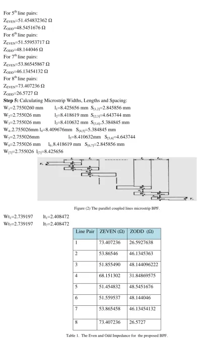
Step 5: Calculating Microstrip Widths, Lengths and Spacing: W1=2.7550260 mm l1=8.425656 mm S[1,2]=2.845856 mm W2=2.755026 mm l2=8.418619 mm S[2,3]=4.643744 mm W3=2.755026 mm l3=8.410632 mm S[3,4]=5.384845 mm W4=2.755026mm l4=8.409676mm S[4,5]=5.384845 mm
W5=2.755026mm l5=8.410632mm S[5,6]=4.643744 W6=2.755026 mm l6=8.418619 mm S[6,7]=2.845856 mm W[7]=2.755026 l[7]=8.425656
Figure (2) The parallel coupled lines microstrip BPF.
Wt1=2.739197 lt1=2.408472 Wt7=2.739197 lt7=2.408472
Line Pair ZEVEN (Ω) ZODD (Ω)
1 73.407236 26.5927638
2 53.86546 46.1345363
3 51.855490 48.144096222
4 68.151302 31.84869575
5 51.454832 48.5451676
6 51.559537 48.144046
7 53.865458 46.13454132
8 73.407236 26.5727
Table 1. The Even and Odd Impedance for the proposed BPF.
proposed filter structure is constructed on the FR4, PCB board with dielectric constant Er= 4:4, and substrate
thickness h = 1:6 mm.
3. Filter Simulation and Results
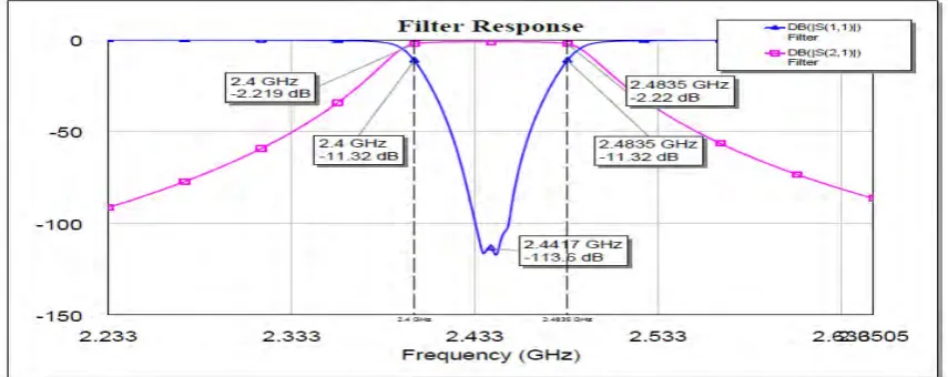
The AWR Microwave Office was used to simulate the BPF design. Figure 4 detailed the dimensional data of the proposed BPF. A step element (offset)was inserted at the junction between the transmission line sections to make the simulated result more accurate. Figure (1) shows the simulated S11, S12, S21 and S22 while figure (5) illustrate the simulated S11, S12, S21 after optimized the proposed design.
Figure (3) The S-parameters Chebyshev, 0.01 ripple LPF.
Figure (4) Response of filter designed by direct calculation, simulated by AWR software. Center frequency is 2.44175GHz. Bandwidth is 0.0835GHz.
4. Conclusion
A coupled line bandpass filter was successfully designed by direct conventional calculation and simulated by using a CAD design tool. The proposed BPF was optimized by using Microwave Office optimizer. Both designs were slightly different due to numerical approximation of direct conventional calculation the attenuation S11 response was observed at 2.44175 GHz with a value of 25 dB and the corresponding Insertion Loss S21 is -1.8dB while the optimized design S11 response at the centre frequency with a value of -113 dB and the corresponding Insertion Loss S21 is -2.2dB. A greater degree of filtration brings about sharper edges in the filter stop band, but the attenuation in the pass band is also increased, due to the greater number of line piars and their losses.Tuning capability would have been a helpful calibration capability to resolve direct conventional calculation. Based on the results that have been obtained from this project, it is proven that the proposed BPF provides better results in term of stopband attenuation and operating frequency.
REFERENCES
[1] R. Levy and J. D. Rhodes, “A comb-line elliptic filter,” IEEE Trans. Microwave Theory Tech. vol. 19, pp. 26-29, Jan. 1971.
[2] M. L. Roy, et. Al., “The continuously varying transmission-line tecnique-application to filter design,” IEEE Trans. Microwave
Theory Tech., vol. 47, pp. 1680-1687, Sept. 1999.
[3] K. C. Lek and K. M. Lum, “Stepped Impedance Key-shaped Resonator for Bandpass and Bandstop Filters Design”, Progress In Electromagnetics Research Symposium Proceedings, KL Malaysia, March 27-30, 2012.
[4] Ian Hunter, “Theory and Design of Microwave Filters”, The Institution of Engineering and Technology, London, United Kingdom, 2006.
[5] George D. Vendelin, Anthony M. Pavio and Ulrich, “Microwave Circuit Design Using Linear and Nonlinear Techniques”, Second Edition, A John Wiley & Sons, Inc., Publication, 2005.
[6] Jia-Sheng Hong, M. J. Lancaster, “Microstrip Filters for RF/Microwave Applications”, John Wiley & Sons, Inc, PP 109, 2001. [7] Kuo-Sheng Chin, Yi-Ping Chen, Ken-Min Lin, and Yi-Chyun Chiang, “Compact Parallel Coupled Line Baned Pass Filter with Wide