International Journal of Emerging Technology and Advanced Engineering
Website: www.ijetae.com (ISSN 2250-2459,ISO 9001:2008 Certified Journal, Volume 4, Issue 8, August 2014)
257
A High Gain and Improved Linearity 5.7GHz CMOS LNA with
Inductive Source Degeneration Topology
Ch. Anandini
1, Ram Kumar
2, F. A. Talukdar
3 1,2,3Department of Electronics & Communication Engineering, NIT Silchar, Assam, India -788010
Abstract— This paper presents a 5.7GHz .18-μm CMOS highly linear and good gain LNA which uses an inductive source degeneration topology to increase linear, gain and save power consumption. The circuit measurement is performed using UMC .18μm CMOS Technology in cadence tool. The LNA exhibits a noise figure of2.5dB, gain of 19.6dB, =-18.dB. Also for =60dBm,40dBm,20dBm, IIP3 are -42.55dBm, -22.61dBmand IIP3=-6dBm respectively, while consuming 5.22mW from1.8V.
Keywords— Cascode amplifiers, inductive source degeneration, post linearization, forward body biasing, Body Biasing Techniques
I. INTRODUCTION
Low noise amplifiers (LNAs) are widely used in high-speed systems. The circuit design of LNAs must balance the specifications of low noise figure, high linearity, large dynamic range, and good impedance matching. LNA is an electronic device comprises of active and passive elements. Passive components are primarily used for biasing and for input/output matching purposes and active devices are chosen such that it can offer high amplification to an input signal with minimum additional noise. There are a wide range of RF transistors that are available for use in high performance LNAs. The choice of an appropriate transistor to meet target specifications is a crucial step in amplifier designing process. Designing a low noise amplifier presents a considerable challenge because of its simultaneous requirement for high gain, low noise figure, good input and output matching and high linearity without oscillation over entire useful frequency range.One of the main target parameter apart from gain and noise figure in designing low noise amplifier is the linearity. This is due the presence of strong inference signals in the input of the LNA. An LNA must be highly linear to prevent the intermodulation tones created by the interference signal. But this linearity improvement should not be done at the expense of the gain or noise figure.
To improve the linearity of the cascode LNA, several linearization methods have been proposed. To suppress the nonlinearity of the amplifier, the third-order derivative coefficient has to be close to zero.
And this can be done by using the optimum gate biasing technique in which a FET can be linearized by biasing at gate to-source voltage at which the third-order derivative of its dc transfer characteristic is zero. But a major drawback of this technique is that the transistor has to be biased at the sweet spot which results into limitation of the transconductance of the input stage leading to reduced gain and increased NF. Another technology for improving the linearity is Feed Forward method which uses two transistors (main and auxiliary) connected in parallel and biased in weak and strong inversion region, respectively. The auxiliary transistor generates a positive third-order derivative of the dc transfer characteristic (gm3) to cancel the negative gm3 generated by the main transistor. This results inincreased linearity with wide DC operating range. But a drawback of this technique is that the additional weak inversion transistor added to achieve linearity degrades the noise performance of the LNA due to its high gate induced current noise getting added to the input. To overcome these drawbacks, a novel post-linearization technique for the cascode CMOS LNA with the concept of IMD sinking is proposed in this paper. In the proposed method, the IMD3 can be partially cancelled by the additional folded diode with a parallel RC circuit.
II. LNATOPOLOGY AND CIRCUIT DESIGN
Low Noise Amplifier Design for 5.7GHz operating frequency range by using .18μm CMOS Technology, where .18μm is the length of device which is the minimum length of device provided by the wander. CMOS Technology is used because of its several advantages such as low cost, low static power dissipation and low area. If we goes to design any analog circuit it is mandatory to known the some design specification and that specification are standard and our goal is to achieve the desirable result.
International Journal of Emerging Technology and Advanced Engineering
Website: www.ijetae.com (ISSN 2250-2459,ISO 9001:2008 Certified Journal, Volume 4, Issue 8, August 2014)
258
Therefore, most of the previous works to improve the linearity of CMOS LNAs have focused on improving the linearity of the CS stage. However, as the operating frequency and the gain increase, the CG stage limits the linearity of the cascode amplifier. To overcome this issue a new CMOS LNA designed is proposed which uses cascode transistor with inductive source degeneration topology
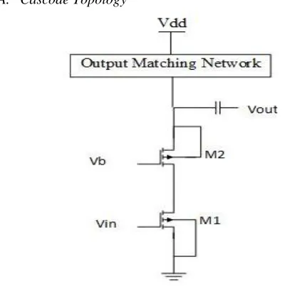
[image:2.612.338.537.147.497.2]A. Cascode Topology
Fig .1 Cascode topology
Cascode transistor topology is a two stage circuit consisting of a transconductance amplifier followed by a buffer amplifier. This topology have a lot of advantages over the single stage amplifier like, better input output isolation, better gain, improved bandwidth, high linearity, higher input impedance, higher output impedance, better stability, higher slew rate etc. Also it reduces the Miller effect.
Cascode topology is generally constructed using FET (field effect transistor) or BJT (bipolar junction transistor). Here one stage will be usually wired in common source/common emitter mode and the other stage will be wired in common base/ common emitter mode.
The width of the transistors are calculated according to the formula –
W
=
(1)
where ω=operating frequency L=length of transistor Cox=oxide capacitance RS=source resistance
B. Input/output stage Matching
Fig .2 Input stage matching circuit
Fig .3 Small signal model of input stage matching circuit
From small signal model we get
[ (
)
]
(2)
Then can be calculated as
(
)
(3)
But for matching we have
(4) Applying this condition we get
(
)
(5) [image:2.612.50.250.228.438.2]
International Journal of Emerging Technology and Advanced Engineering
Website: www.ijetae.com (ISSN 2250-2459,ISO 9001:2008 Certified Journal, Volume 4, Issue 8, August 2014)
259
Using these equation the value of and is calculated at 5.5GHz.
The most important part of an LNA design is the output impedance stage. As the output of the LNA is feed to the mixer so as to propagate the signal from one block to another block, there should be sufficient impedance matching in between the blocks.
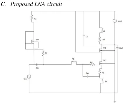
[image:3.612.323.559.148.314.2]C. Proposed LNA circuit
Fig .4 Proposed LNA circuit
The proposed LNA shown in the figure employed inductive source degeneration in which inductor , is connected to the source of M0. An advantage of this method is that it has greater control over the value of the real part of the input impedance through the choice of inductance. Here , , and are all implemented with on-chip spiral inductors. is gate inductor which is used for tuned out the effect of input capacitance and is source degeneration inductor used for input match and is drain inductor which provide output resonance with output capacitance and also play an important role in achieving high gain. The inductors and are chosen in such a way that it provide the desired input resistance. M3, R1 and R2 formed the biased circuit where transistor M3 essentially forms a current mirror with M1 and its width is a small fraction of the width of M1 .Current mirror transistor M3 is used to minimize the power overhead of the bias circuit. The current mirror helps in temperature-stabilization of the circuit. The value of R2 is adjusted to fix the operating point and which are DC blocking capacitors.
From the above fig we get
=
+
+
(7)
=
(8)
|
|
=
=
(9)
|
|
=
Q
(10)
=
Q+
Q+
Q
(11)
IIP3=
(12)
IIP3=
(13)
From the above equation we know that we need a capacitor between S (source) and G (gate) in order to have a small Q.IP3 and large
[image:3.612.47.256.222.403.2]III. SIMULATION RESULTS
Fig .6 Input impedance match,
[image:3.612.334.545.400.598.2]International Journal of Emerging Technology and Advanced Engineering
Website: www.ijetae.com (ISSN 2250-2459,ISO 9001:2008 Certified Journal, Volume 4, Issue 8, August 2014)
[image:4.612.324.554.127.331.2]260 Fig .8 Gain
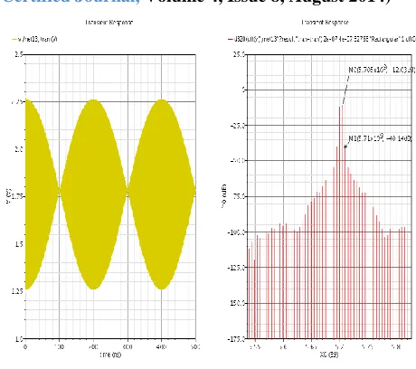
Fig .9 IIP3=-42.55dBm for Pin=-60dBm
Fig .10 IIP3=-22.61dBm for Pin=-40dBm
Fig .11 IIP3=-6dBm for Pin=-20dBm
The proposed LNA was designed for 5.7 GHz operation in cadence 0.18-μm CMOS technology. The measured characteristics of , Noise figure (NF) verse frequency
for the LNA are shown in the Fig. 6amd 7. And the obtained values are =-18.46db and NF=2.5dB
respectively. Fig. 8 shows the maximum gain of 19.63dB at 5.7 GHz. Improved linearity for different Pin are also shown. The proposed LNAs consume only 5.22mW power with a supply voltage of 1.8 V.
TABLEI
SIMULATED PERFORMANCE OF THE PROPOSED LNA
Frequency (GHz)
Noise Figure(dB)
Gain (dB)
Power
consumption(mW) (dBm)
5.7 2.5 19.6 5.22 -18.46
TABLEII
DIFFERENT VALUES OF IIP3 AT DIFFERENT PIN VALUES
IIP3(dBm) at 5.7 GHz
Pin=-60dBm Pin=-40dBm Pin-20dBm
-42.55 -22.61 -6
[image:4.612.60.277.132.453.2] [image:4.612.53.277.474.636.2] [image:4.612.318.572.481.608.2]International Journal of Emerging Technology and Advanced Engineering
Website: www.ijetae.com (ISSN 2250-2459,ISO 9001:2008 Certified Journal, Volume 4, Issue 8, August 2014)
261
IV. CONCLUSION
In order to design any circuit, it is always better to abstract away its complexity. In this design a low noise amplifier for 5.7GHz applications covered all the important details required for the general low noise amplifier And also a novel low noise amplifier is designed and simulated keeping view of high gain and linearity for given frequency applications. This design used cascode inductive source degeneration topology as it provided good matching and high gain as compared to other topology. After the simulation we achieved Gain 19.6dB, Noise Figure 2.5dB, and power consumption 5.22mW with very improved linearity for different values and supply voltage is 1.8v.
Acknowledgment
This work is carried out at National Institute of Technology Silchar. We are thankful to Prof. F.A.Talukdar for his support.
REFERENCES
[1] X. Fan, E. Sánchez-Sinencio, and J. Silva-Martinez, ―A 3 GHz–10 GHz common gate ultrawideband low noise amplifier,‖ in Proc. IEEE Midwest Symp. Circuits and Systems, Aug. 2005, pp. 631– 634..
[2] T.-S. Kim and B.-S. Kim, ―Post-linearization of cascode CMOS LNA using folded PMOS IMD sinker,‖ IEEE Microw. Wireless Comp. Lett., vol. 16, no. 4, pp. 182–184, Apr. 2006.
[3] N. Kim, V. Aparin, K. Barnett, and C. Persico, ―A cellular-band CDMA CMOS LNA linearized using active post-distortion,‖ IEEE J.Solid-State Circuits, vol. 41, no. 7, pp. 1530–1534, Jul. 2006. [4] H. Zhang, X. Fan, and E. Sánchez-Sinencio, ―A low-power,
linearized,ultra-wideband LNA design technique,‖ IEEE J. Solid-State Circuits, vol. 44, no. 2, pp. 320–330, Feb. 2009.
[5] T. H. Lee, The Design of CMOS Radio-Frequency Integrated Circuits. Cambridge, U.K.: Cambridge Univ. Press, 1998.
[6] S. Ganesan, E. Sánchez-Sinencio, and J. Silva-Martinez, ―A highly linear low noise amplifier,‖ IEEE Trans. Microw. Theory Tech., vol. 54, no. 12, pp. 4079–4085, Dec. 2006.
[7] B. Razavi, RF Microelectronics. Prentice Hall, 1998
[8] B. Kim, J.-S. Ko, and K. Lee, ―A new linearization technique for MOSFET RF amplifier using multiple gated transistors,‖ IEEE Microwave and Guided Wave Letters, vol. 10, pp. 371–373, Sept 2000.
[9] T. W. Kim, B. Kim, and K. Lee, ―Highly linear RF CMOS amplifier and mixer adopting MOSFET transconductance linearization by multiple gated transistors,‖ IEEE Radio Frequency Integrated Circuits Symposium, pp. 107–110, June 2003
[10] X. Fan, H. Zhang, and E. Sánchez-Sinencio, ―A noise reduction and linearity improvement technique for a differential cascode LNA,‖ IEEEJ. Solid-State Circuits, vol. 43, no. 3, pp. 588–599, Mar. 2008. [11] Zhang, C., D. Huang, and D. Lou, \Optimization of cascade CMOS
low noise amplifier using interstage matching network,"Proc. Electron. Devices and Solid State Circuit Conf., 465-468,Dec. 2003 [12] Heng Zhang, Student Member, IEEE, and Edgar Sánchez-Sinencio,