5
X
October 2017
Rectangular Patch Antenna Array Slotted Design
for Triple Band Using HFSS
Pankaj Beniwal1, Ravinder S. Bisht2, Kapil Arora3
1
M.Tech Scholar, ECE Department, R.P.I.I.T (Bastara), Karnal
2 ,3
Assistant Professor, ECE Department, R.P.I.I.T (Bastara), Karnal
Abstract: The proposed antenna can be suitably employed for satellite to earth communication. The proposed antenna covers the X-band satellite downlink as well as uplink frequency bands making it suitable to be employed for X band satellite communication applications. The specified frequency ranges of 13 GHz (Ku-band) can also be employed for military satellite, weather satellite and radio-determination purposes. Antenna also covers the K-Band as well as Ka-Band applications. The Results will show good impedance matching, good radiation patterns in the operating band. Thus, this antenna is a good applicant for wireless communication applications which includes long distance radio telecommunications like cordless telephones, some Wi-Fi devices, weather radar systems, direct broadcast satellite.
In this paper, a microstrip patch antennas for a dual frequency 10.55 and 14.59 GHz (that cover X-Band and Ku-Band) and triple frequency 11.54 GHz, 13.95 GHz, 23.48 GHz (that also cover X-Band, Ku-Band and K-Band) with only coaxial probe feeding technique is presented. The various parameters like return loss, radiation pattern, smith chart, electric field and VSWR are plotted for each antenna. The affect of various parameters like patch length, MSL length have been studied.
Keywords: Dual band, Triple Band.Slotted Patch Array Shape, Microstrip patch antenna,S-Parameters, smith chart, bandwidth, VSWR, resonant frequency,HFSS13.0.
I. INTRODUCTION
Antenna is the most fundamental block of the wireless communication. Recently, the growth of wireless systems leads to a lot of innovations in the Microstrip antenna designs. Microstrip patch antenna has become an integral part of these devices working in ultra to super high frequency ranges. The patch and slot are the two parameters which affect the overall antenna’s performance [1]. Microstrip antenna technology began its rapid development in the late 1970s. By the early 1980s basic microstrip antenna elements and arrays were fairly well establish in term of design and modeling. In the last few years patch antennas have been largely studied due to their advantages over other radiating systems, which include light weightiness, reduced size, low cost, conformability and the ease of integration with active device [3].
Microstrip patch antenna is basically made of thin sheet of insulating material called dielectric substrate. It is back bone of circuit because it provides a support to strip and patch. The radiating patch and the feed lines are usually photo etched on the dielectric substrate. Microstrip patch antennas radiate primarily because of the fringing fields between the patch edge and the ground plane.. One major drawback of microstrip patch antennas is their narrow bandwidth and low gain. It has been established that the slotted patch can significantly improve the bandwidth of the microstrip antenna. The slotted patch antenna can be designed not only for wideband applications, but also for dual-band and, triple-band application with small and wide frequency ratios.. The IEEE 802.16 WiMAX standard allows data transmission using multiple broadband frequency ranges. The original 802.16a standard specified transmissions in the range 10 - 66 GHz, but 802.16d allowed lower frequencies in the range 2 to 11 GHz. The lower frequencies used in the later specifications means that the signals suffer less from attenuation and therefore they provide improved range and better coverage within buildings[3].
uncomplicated manner and its overall cost be less and it need to have certain amount of compatibility with looped surfaces. But, stability is still one of the important properties of coming up application [6]. Microstrip patch antenna is the most suitable and prevalent type of antenna in use today, their effective frequency range is in between 1GHz to 10 GHz. Since 1970s this antenna has been flourishing, where its size and performance were very effective as conversation entity was required at these frequencies. The architecture of the microstrip patch antenna consists of the substrate of which below is the ground plane and above is the patch. These antennas find applications in mobiles instruments, receivers using GPS technologies and other wireless and wired products reason being there high values of dielectric constant and additional size reduction. Since this antenna has flat profile and is light in weight also makes them suitable for applications like airborne and spacecraft [6].
II. ANALYSIS OF ANTENNA
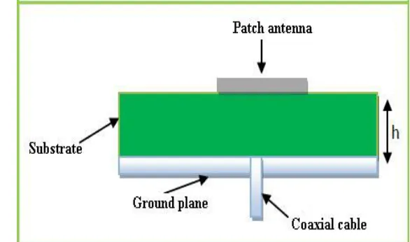
[image:3.612.161.470.254.396.2]The length of the patch is denoted by L and width of the patch is denoted by W. Because the dimensions of the patch are finite along the length and width, the fields at the edges of the patch undergo fringing. Since some of the waves travel in the substrate and some in air, an effective dielectric constant is introduced to account for fringing and the wave propagation in the line.
Figure 1 Basic Geometry of Microstrip Patch Antenna A. Coaxial Feed
A Coaxial Fed antenna consists of a microstrip patch fed by the center conductor of a coaxial line (see figure 2). The outer coaxial conductor is electrically connected to the ground plane. Due to the absence of a microstrip feed line, the substrate thickness and permittivity can be designed to maximize antenna radiation. However, the probe center conductor underneath the patch causes undesired distortion in the electric field between the patch and ground plane and produces undesired reactive loading effects at the antenna input port [1]. The undesired reactance can be compensated by adjusting the probe location on the patch. It suffers from the drawbacks of narrow bandwidth, difficult to model specially for thick substrate and possess inherent asymmetries which generate higher order modes which produce cross polarization radiation[1,2].
[image:3.612.163.456.546.719.2]III. DESIGNINGOF ANTENNA
A. Designing of proposed microstrip patch antenna
[image:4.612.99.515.114.358.2]The geometry of proposed antenna which is coaxial probe fed for wireless application is depicted in figure 3
Figure 3 Designing with coaxial feed B. Results
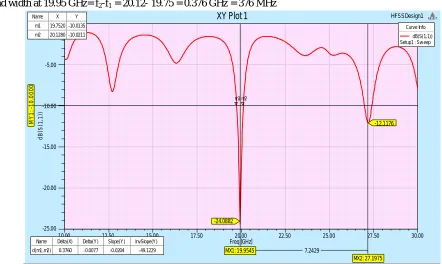
1) Observation from -10dB return loss
a) Resonant frequency =19.95 GHz at -24.088 dB and 27.19 at -12.11dB b) Band width at 19.95 GHz= f2-f1 = 20.12- 19.75 = 0.376 GHz = 376 MHz
Figure 4 Return loss graph of coaxial feed 2) Observation from VSWR
a) VSWR at resonant frequency 19.95 GHz=1.13 which is good for practical antenna.
10.00 12.50 15.00 17.50 20.00 22.50 25.00 27.50 30.00
Freq [GHz] -25.00
-20.00 -15.00 -10.00 -5.00 0.00
d
B
(S
(1
,1
))
HFSSDesign1
XY Plot 1 ANSOFT
M
Y
1
:
-1
0
.0
0
0
0
MX1: 19.9545
m1 m2
MX2: 27.1975 -24.0882
-12.1176
7.2429
Curve Info
dB(S(1,1)) Setup1 : Sw eep
Name X Y
m1 19.7520 -10.0135
m2 20.1280 -10.0211
Name Delta(X) Delta(Y) Slope(Y) InvSlope(Y)
[image:4.612.74.516.427.691.2]Figure 5 VSWR graph of coaxial feed 3) Radiation Pattern
Figure 6 Radiation pattern graph of coaxial feed
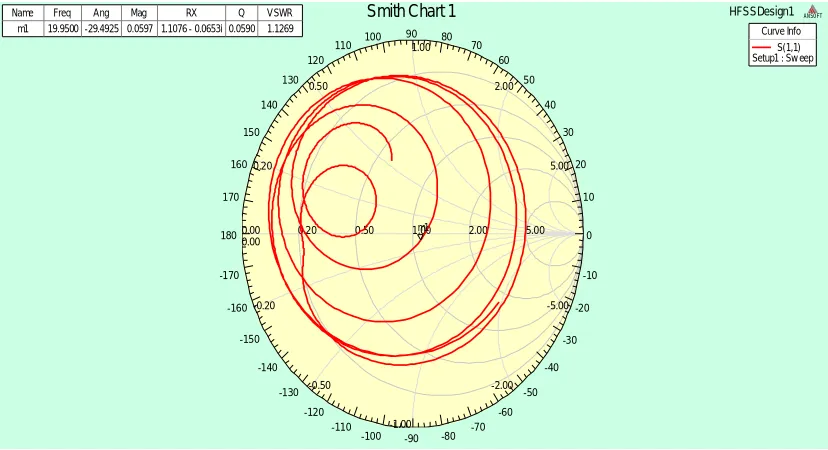
[image:5.612.101.515.496.721.2]4) Smith Chart: The smith chart gives 1.1076×50= 55.38 ohm impedance which is good as near to match the characteristic impedance of value of 50 ohm.
Figure 7 Smith chart graph of coaxial feed
10.00 12.50 15.00 17.50 20.00 22.50 25.00 27.50 30.00
Freq [GHz] 0.00 2.50 5.00 7.50 10.00 12.50 15.00 17.50 V S W R (1 ) HFSSDesign1
XY Plot 2 ANSOFT
M Y 1 : 2 .0 0 0 0 MX1: 19.9545 1.1332 Curve Info VSWR(1) Setup1 : Sw eep
5.00 2.00 1.00 0.50 0.20 0.00 5.00 -5.00 2.00 -2.00 1.00 -1.00 0.50 -0.50 0.20 -0.20 0.00 0 10 20 30 40 50 60 70 80 90 100 110 120 130 140 150 160 170 180 -170 -160 -150 -140 -130 -120 -110
-100 -90 -80 -70 -60 -50 -40 -30 -20 -10 HFSSDesign1
Smith Chart 1 ANSOFT
m1
Curve Info S(1,1) Setup1 : Sw eep Name Freq Ang Mag RX Q V SWR
B. Design of Proposed Dual Band Antenna using DGS
[image:6.612.76.540.131.283.2]In this design we have reduced the size of ground dimension in X-direction to design a effective dual band antenna.In this technique, microstrip patch antenna is designed using coaxial probe feed and some changes in boundary conditions of above antenna to get desired results:
Figure 8 Designing of proposed dual band antenna 1) Observation from -10dB return loss
[image:6.612.68.517.310.477.2]a) Resonant frequency =10.55 GHz at -21.52dB( S-parameter) b) Resonant frequency =14.59 GHz at -37.97dB( S-parameter)
Figure 9 Return loss graph of Proposed dual antenna 2) Observation from VSWR
a )VSWR at resonant frequency 10.55 GHz=1.17 b)VSWR at resonant frequency 14.59 GHz=1.02
Figure 10 VSWR graph of Proposed dual Antenna
8.00 9.00 10.00 11.00 12.00 13.00 14.00 15.00 16.00
Freq [GHz] -40.00 -35.00 -30.00 -25.00 -20.00 -15.00 -10.00 -5.00 0.00 d B (S (1 ,1 )) HFSSDesign1
XY Plot 1 ANSOFT
M Y 1 : -1 0 .0 0 0 0 MX1: 10.5564 MX2: 14.5911 m1 m2 -21.8279 -37.9777 4.0347 Curve Info dB(S(1,1)) Setup1 : Sw eep
Name X Y
m1 10.3830-10.0043
m2 10.7150-10.0027
8.00 9.00 10.00 11.00 12.00 13.00 14.00 15.00 16.00
Freq [GHz] 0.00 2.50 5.00 7.50 10.00 12.50 15.00 17.50 20.00 22.50 V S W R (1 ) HFSSDesign1
XY Plot 2 ANSOFT
[image:6.612.101.518.533.719.2]3) Radiation Pattern
Figure 11 Radiation pattern curve of Proposed Dual Antenna 4) Smith Chart
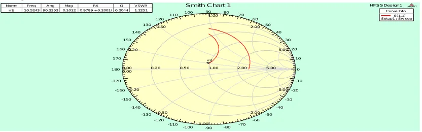
[image:7.612.101.517.261.391.2]The smith chart curve of Proposed Antenna is shown in Figure. Impedance Matching = 0.9789 ×50= 48.95 ohm
Figure 12 Smith chart curve of Proposed dual antenna C. Design of Proposed Triple Band Antenna using slotted patch and DGS:
[image:7.612.85.530.474.630.2]It is observed from the above model bands in designing microstrip patch antenna has been increased so we are using four slots with same size in patch plane that is single in each small rectangular patch (small patches which make array) and there is four array without any lot or DGS has been introduced in simple reference antenna design. The total three bands are achieved in this case.
Figure 13 Designing for Triple band D. Results
1) Observation from -10dB return loss
a) Resonant frequency = 11.54 GHz at -13.80dB( S-parameter) b) Resonant frequency = 13.95 GHz at -17.49dB( S-parameter) c) Resonant frequency = 23.48 GHz at -14.26dB( S-parameter)
5.00 2.00 1.00 0.50 0.20 0.00
5.00
-5.00 2.00
-2.00 1.00
-1.00 0.50
-0.50 0.20
-0.20
0.00 0
10 20 30 40 50 60 70 80 90 100 110 120
130
140
150
160
170
180
-170
-160
-150
-140
-130
-120 -110
-100 -90 -80 -70
-60 -50
-40 -30
-20 -10
HFSSDesign1
Smith Chart 1 ANSOFT
m1
Curve Info S(1,1) Setup1 : Sw eep
Name Freq Ang Mag RX Q VSWR
Figure 14 Return loss graph of proposed triple band antenna 2) Observation from VSWR
[image:8.612.93.517.297.511.2]a) VSWR at resonant frequency 11.54 GHz =1.51 b) VSWR at resonant frequency 13.95 GHz =1.30 c) VSWR at resonant frequency 23.48 GHz =1.47
Figure 15 VSWR graph of Proposed triple band antenna 3) Radiation Pattern
Figure 16 Radiation pattern curve of Proposed triple band antenna
7.50 10.00 12.50 15.00 17.50 20.00 22.50 25.00 27.50 30.00
Freq [GHz] -17.50 -15.00 -12.50 -10.00 -7.50 -5.00 -2.50 0.00 d B (S (1 ,1 )) HFSSDesign1
XY Plot 1 ANSOFT
M Y 1 : -1 0 .0 0 0 0 m2 m3 m1
Curve Inf o
dB(S(1,1)) Setup1 : Sw eep
Name X Y
m1 11.5400 -13.8071
m2 13.9586 -17.4911
m3 23.4837 -14.2678
7.50 10.00 12.50 15.00 17.50 20.00 22.50 25.00 27.50 30.00
Freq [GHz] 0.00 2.00 4.00 6.00 8.00 10.00 12.00 14.00 16.00 V S W R (1 ) HFSSDesign1
XY Plot 2 ANSOFT
M Y 1 : 2 .0 0 0 0 m3 m2 m1 Curve Info VSWR(1) Setup1 : Sw eep
Name X Y
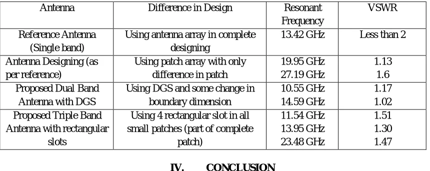
Table 1 Difference Table between Reference and Proposed antenna Antenna Difference in Design Resonant
Frequency
VSWR Reference Antenna
(Single band)
Using antenna array in complete designing
13.42 GHz Less than 2 Antenna Designing (as
per reference)
Using patch array with only difference in patch
19.95 GHz 27.19 GHz
1.13 1.6 Proposed Dual Band
Antenna with DGS
Using DGS and some change in boundary dimension
10.55 GHz 14.59 GHz
1.17 1.02 Proposed Triple Band
Antenna with rectangular slots
Using 4 rectangular slot in all small patches (part of complete
patch) 11.54 GHz 13.95 GHz 23.48 GHz 1.51 1.30 1.47 IV. CONCLUSION
In this research paper, a microstrip patch antennas for a dual frequency 10.55 and 14.59 GHz (that cover X-Band and Ku-Band) and triple frequency 11.54 GHz, 13.95 GHz, 23.48 GHz (that also cover X-Band, Ku-Band and K-Band) with only coaxial probe feeding technique is presented. The various parameters like return loss, radiation pattern, smith chart, electric field and VSWR are plotted for each antenna.
REFERENCES
[1] Ramesh Garg, PrakashBhartie, InderBahl, ApisakIttipiboon, “Microstrip Antenna Design Handbook”, Artech House Inc. Norwood, MA, 2009, pp. 1-68, 253-316.
[2] Ahmed FatthiAlsager , “Design and Analysis of Microstrip Patch Antenna Arrays”, M.Tech Thesis in Electrical Engineering– Communication and Signal processing 2011, University College of Boras School of Engineering, SE‐501 90 BORAS.
[3] Sanjeevdwivedi and R.N.Yadav, “Design Of U-Shape Microstrip Patch Antenna For Wimax Applications At 2.5 Ghz”, 978-1-4673-5999-3/13/2013 IEEE. [4] N. Ramli, M. T. Ali, A. L. Yusof, and N. Ya’acob, “Frequency Reconfigurable Stacked Patch Microstrip Antenna (FRSPMA) for LTE and WiMAX
Applications”, 978-1-4673-2088-2013 IEEE
[5] Rui Ma, Pei ZhengMengjiaLuo, Zhilei Wen, Houjun Sun, “Design of W band Dual Polarized Microstrip Patch Antenna” IEEE, 2014 3rd Asia-Pacific Conference on Antennas and Propagation
[6] Vinita Mathur, “Comparison of Performance Characteristics of Rectangular, Square and Hexagonal Microstrip Patch Antennas”, IEEE 978-1-4799-6896-1/14/2014.
[7] R.Bargavi,K.Sankar and S.Arivumani Samson , “Compact Triple band H-Shaped Slotted Circular Patch Antenna”, International Conference on Communication and Signal Processing IEEE, April 3-5,2014, India.
[8] H.Liu, Z. Li, and X. Sun, “Compact defected ground structure in microstrip technology,” Electron. Lett., Vol. 41, No. 3, 132–134, 2009.
[9] S.W.Ting, K.W. Tam, and R. P. Martins, “Compact microstrip quasi-elliptic bandpass filter using open-loop dumbbell shaped defected ground structure,” IEEE MTT-S Int. Microwave Symp.Digest, 527–530, 2010.
[10] M. K.Mandal and S. Sanyal, “A novel defected ground structure for planar circuits,” IEEE Microwave Compon. Lett., Vol. 16, No. 2, 93–95, 2010.
[11] K.P. Yang, K.L. Wong, "Dual-band Circularly-polarized Square MicrostripAntenna,"IEEE Trans. Antennas Propagation, vol. 49, no.3, pp. 377-382, March 2010.
[12] Macro A.Antoniades, and George V. Eleftheriades, “A Compact Multiband Monopole Antenna with a Defected Ground Plane,” IEEE, Antennas and Wireless Propagation Letters, Vol.7, 2011.
[13] Joseph Costan Tine1, Karim Y. Kabalan, Al EI-Hajj, MohammadRammal “New Multi-Band Microstrip Antenna Design For Wireless Communications” Vol. 49, No. 6,2011.
[14] Abdel Fattah Sheta, Ashraf S. Mohra, And Samir F. Mahmoud “Modified Compact H-Shaped Microstrip Antenna For Tuning Multi-Band Operation”, 2011. [15] L. M. Si And X. Lv, “CPW-Fed Multi-Band Omni-Directional Planar Microstrip Antenna Using Composite Metamaterial Resonators For Wireless
Communications” Pier 83, 133–146, 2012.
[16] P.Mythili, Philip Cherian, S.Mridula, Binu Paul “Design Of A Compact Multiband Microstrip Antenna”, 2012. [17] PramendraTilanthe, P. C. Sharma “Design of A Single Layer Multiband Microstrip Square Ring Antenna”, 2012.
[18] Muhammad R. Khan, Mohamed M. Morsy, Muhammad Z. Khan and Frances J. Harackiewicz “Miniaturized Multiband Planar Antenna for GSM, UMTS, WLAN and Wimax Bands” 2013.
[19] Halappa R. Gajera, Anoop C.N, M. M. Naik. G, Archana S. P, Nandini R Pushpitha B.K, Ravi Kumar M.D, “The Microstrip Fed Rectangular Microstrip Patch Antenna(RMPA) with Defected Ground Plane for HIPERLAN/1” IJECT Vol. 2, Issue 3, Sept. 2013
[20] ZuhuraJuma Ali, “A Miniaturized Ultra Wideband (UWB) Antenna Design for Wireless Communications” International Journal of Scientific & Research Publications, Vol 4, Issue 7, July 2014.
[21] A. Gnandeepreddy, k. Gopivasanthkumar, “Design And Simulation Of A L And U‐Shaped Slot Compact Planar Monopole Antenna”, International Journal of Science, Engineering and Technology, 2014.
[23] UditRaithatha, S. SreenathKashyap& D. Shivakrishna, May 2015, “Swastika Shaped Microstrip Patch Antenna for ISM Band Applications” international journal IRJET.
[24] Sumeet Singh Bhatia, Jagtar Singh Sivian, ManpreetKaur, “Comparison of feeding techniques for the design of microstrip rectangular patch antenna for x-band applications”, International Journal of Advanced Technology in Engineering and Science, Volume No.03, Special Issue No. 02, 2015.