International Journal of Emerging Technology and Advanced Engineering
Website: www.ijetae.com (ISSN 2250-2459,ISO 9001:2008 Certified Journal, Volume 3, Issue 4, April 2013)
332
Comparison of PWM and One-Cycle Control for Switching
Converters
Binitha P M
1, T G Sanish Kumar
21 M.Tech Student, 2Assistant Professor, Dept. of Electrical & Electronics Engg., Govt. Engineering College. Thrissur, Kerala,
India
Abstract— Conventional PWM control scheme has slow dynamic response to power source perturbation. Another modulation strategy called one-cycle control overcomes this inherent drawback of PWM control and achieves good power source perturbation rejection and fast dynamic response. In this paper the comparison between PWM and one-cycle control is carried out in terms of steady-state and dynamic response. Simulation results are provided to verify the conclusions.
Keywords— Integrator, Nonlinear control, One-cycle control, PWM control, Switching converters.
I. INTRODUCTION
Switching converters are pulsed nonlinear dynamic systems. Such systems under pulsed nonlinear control should be more robust, have faster dynamic response and provide better rejection of power source perturbation than the same systems under linear feedback control.
In pulse width modulation (PWM) control, the duty ratio is linearly modulated in a direction that reduces the error. When the input voltage is perturbed, that must be sensed as an output voltage change and error produced in the output voltage is used to change the duty ratio to keep the output voltage to the reference value. This means it has slow dynamic performance in regulating the output in response to the change in input voltage. A large number of switching cycles is required before steady-state is regained.
One-cycle control (OCC) technique is a nonlinear control method, which takes advantage of the pulsed and nonlinear nature of the switching converters and achieves instantaneous dynamic control of the average value of the switched variable [1],[2]. More specifically it takes only one switching cycle for the average value of the switched variable to reach a new steady-state after a transient. There is no steady-state or dynamic error between the control reference and the average value of the switched variable. This technique provides fast dynamic response, excellent power source disturbance rejection, robust performance, and automatic switching error correction. It has been widely applied in dc-dc conversion [3], power amplifier [4], power factor correction [5], active power filter [6], multi-input converters [7], and maximum power point tracking (MPPT) of PV solar energy [8].
The objective of this paper is to compare the PWM and one-cycle control for switching converters based on the analysis of buck converter with PWM and one-cycle control. Both control schemes are discussed in terms of steady-state response, input source and load transient response using MATLAB/ simulink simulation.
This paper is organized as follows. The PWM technique is briefly reviewed in section II. Section III describes the one-cycle control technique. Section IV discusses the simulation procedure and comparisons. Finally conclusions are given in section V.
II. PULSE WIDTH MODULATION (PWM)CONTROL
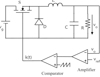
[image:1.612.366.531.453.580.2]In PWM control, the duty ratio pulses are produced by comparing control reference signal with a saw-tooth signal. As a result the control reference is linearly modulated into the duty ratio signal. A buck converter with PWM control is shown in Fig. 1. The duty ratio is modulated in a direction that reduces the error.
Fig. 1 Buck converter with PWM control
International Journal of Emerging Technology and Advanced Engineering
Website: www.ijetae.com (ISSN 2250-2459,ISO 9001:2008 Certified Journal, Volume 3, Issue 4, April 2013)
333 A large number of switching cycles is required before the steady-state is reached. The output is always influenced by the input voltage perturbation.
III. ONE-CYCLE CONTROL
A. One-Cycle Control Theory
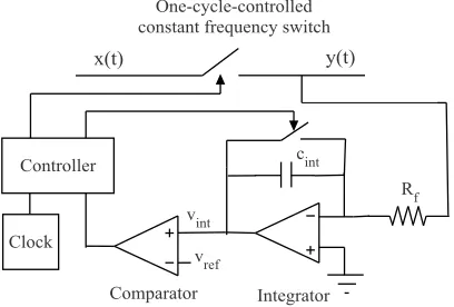
[image:2.612.71.561.128.723.2]The theory of one-cycle control is shown in Fig. 2. Fig.3 shows its operating waveforms.
Fig. 2 One-cycle controlled constant frequency switch
Fig. 3 The waveforms of the one-cycle controlled constant frequency switch
The switch function is
0 1
( ) . (1)
0
ON
ON S
t T
k t
T t T
In each cycle, the switch is on for a time duration ON
T
and is off for a time duration OFF
T , where
=
ON OFF
T T switching period S
T , the duty ratio
ON S T d T .
From Fig. 2 we know,
( ) ( ) ( ). (2)
y t k t x t
The average of the switched variable is
0
1
( ) ( ) ( ). (
() 3)
ON T
S
x t dt
t x t d t
T
y
The switched variable y t( ) at the output of the switch is the product of the input signal x t( ) and the duty ratio d t( ); therefore, the switch is nonlinear.
If the duty ratio of switch is modulated such that the integration of the switched variable at the switch output is exactly equal to the integration of the control reference in each cycle, i.e.
0 0
( ) ( ) (4)
ON S
T T
ref
x t dt v t dt
then 0 0 1 1 ( ) ( ) ( ). ( ) 5) ( ON S T T ref S S refx t dt v t dt
T T
v t
y t
With one-cycle control, the effective output signal of the switch is
( ). (6
) )
( ref t
y t v
The one-cycle controller is comprised of an integrator with reset, a comparator, a flip-flop, a clock and an adder. The integration starts the moment when the switch is turned on by the fixed frequency clock pulse.
The integration value,
int 0
is const
( ). ant. )(7 t
k v k x t dt
When int
v reaches the control referencevref( )t , the controller sends a command to the switch to change it from on state to off state. The duty ratio of the present cycle is determined by the following equation:
0
( ) . (8)
s dT
ref
[image:2.612.70.274.247.385.2]International Journal of Emerging Technology and Advanced Engineering
Website: www.ijetae.com (ISSN 2250-2459,ISO 9001:2008 Certified Journal, Volume 3, Issue 4, April 2013)
334 The average value of the switched variable at the switch output is given by
0
1 1
( ) (9)
s dT
ref c ref
S S
y t x t dt v t k v t
T kT
Where 1
c s
k kT
.
That is in one-cycle control, the duty ratio of the switch is modulated such that in each cycle the average value of the switched variable is exactly equal to or proportional to the control reference in the steady state or in a transient.
B. One-Cycle Control of Buck Converter
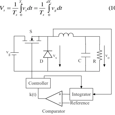
One-cycle control of buck converter is shown in Fig.4. The dc source voltage is
g
v and the switch S is operated with a constant frequency fS.The power source voltage is
chopped by the switch resulting in a switched variable vS. Close observation of the switched variable leads to a simple fact. The output voltage of the buck converter is the average value of the switched variable.
0 0
1 1
(10)
s s
T dT
s s g
s s
V v dt v dt
T T
[image:3.612.68.271.382.584.2]
Fig. 4 One-cycle control of buck converter
A constant frequency clock simultaneously turns on the MOSFET and activates the integrator at the beginning of each switching period. The diode voltage is integrated and compared with control reference. When the integrated diode voltage reaches the control reference, the comparator changes its state. As a result the MOSFET is turned off and the integrator is reset to zero.
With this control scheme, the duty ratio d is determined by
0
(11) 1 dTs
g ref
s
v dt v
T
Which is a nonlinear function of the power source voltage and control reference. The duty ratio d of the current switching cycle is independent of the state of previous switching cycles; therefore, the transient of the average value of the switched variable is completed within one switching cycle.
IV. SIMULATION RESULTS
The comparison of PWM and one-cycle control is demonstrated by MATLAB/simulink simulation. The MATLAB model for buck converter using PWM and OCC are shown in Fig.5 and Fig.6 respectively. In PWM control, PI controller should be redesigned until the stability as well as the dynamic responses satisfy the requirements. But with OCC, PI controller is not required so the design of the closed loop is greatly simplified.
The specifications used for simulation are listed below.
1)Switching frequency S
f 100 KHz. 2)Output filter inductor,
f
L 1.38 mH. 3) Parasitical resistor of ( )
f
f L
L R 0.2 Ω.
4)Output filter capacitor,Cf=220 µF.
5)Parasitical resistor of ( ) f
f C
[image:3.612.339.555.392.657.2]C R 0.29 Ω. 6)Load resistance, R= 25 Ω.
International Journal of Emerging Technology and Advanced Engineering
Website: www.ijetae.com (ISSN 2250-2459,ISO 9001:2008 Certified Journal, Volume 3, Issue 4, April 2013)
[image:4.612.53.289.93.313.2]335
Fig. 6 Buck converter using one-cycle control
C. Steady State Analysis
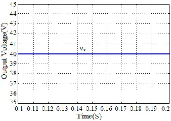
[image:4.612.349.536.213.350.2]The simulation is done at a constant input voltage, constant control reference and load. Then the output voltage of the buck converter using PWM and OCC techniques are shown in Fig. 7 and Fig.8. From the simulation results, we can see, both PWM and OCC techniques provide very good steady-state performance.
Fig. 7 Output voltage under PWM control
Fig. 7 Output voltage under one-cycle control
D. Power Source Perturbation Analysis
[image:4.612.347.537.370.517.2]The simulation results corresponding to the power source disturbance from 50V to 65V at constant control reference and load are shown in Fig.9 and Fig.10. Fig.9 shows the power source voltage and output voltage using PWM control; the power source voltage and output voltage using one-cycle control is shown in Fig.10.
[image:4.612.87.253.435.551.2]Fig. 9 The power source and output voltage using PWM control
Fig. 10 The power source and output voltage using one-cycle control
In the above simulation waveforms we can see, a buck converter under PWM control has slow dynamic performance in regulating the output in response to the change in input voltage. Output voltage is changed due to input voltage perturbation. But one-cycle control breaks this drawback of PWM control. Under one-cycle control, the output voltage do not change even if the power source having a disturbance. So one-cycle control technique is excellent to reject the power source disturbance.
E. Load Perturbation Analysis
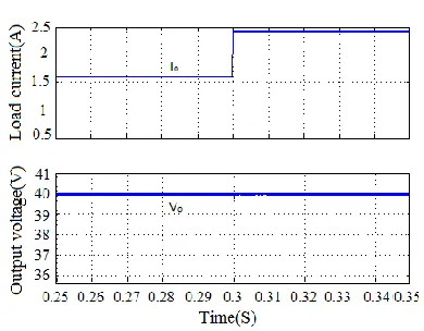
[image:4.612.85.254.585.704.2]International Journal of Emerging Technology and Advanced Engineering
Website: www.ijetae.com (ISSN 2250-2459,ISO 9001:2008 Certified Journal, Volume 3, Issue 4, April 2013)
[image:5.612.74.265.127.269.2]336
Fig. 11 The load current and output voltage using PWM control
Fig. 12 The load current and output voltage using one-cycle control
V. CONCLUSION
PWM and one-cycle control techniques are compared in terms of steady-state and dynamic response. The simulation results have demonstrated that, under both control techniques switching converter can have good steady state performance but one-cycle control shows better performance than PWM control in dynamic response and thereby overcomes the inherent drawback of PWM control.
One-cycle control is a powerful nonlinear control method for switching circuits and systems. It provides fast dynamic tracking and excellent perturbation rejection.
REFERENCES
[1] Keyue. M. Smedley and C. Slobodan, “One-cycle control of switching converters,” IEEE Transactions on Power Electronics, vol. 10, no. 6, Nov.1995.
[2] Yong Wang and Songhua Shen, “Research on one-cycle control for switching converters” Proceedings of the 5th world congress on Intelligent control and Automation, June15-19,2004, Hangzhou, P.R.China.
[3] K. M. Smedley and C. Slobodan, “Dynamics of one-cycle controlled Cuk converters,” IEEE Transactions on Power Electronics, vol. 10, no. 6, Nov. 1995.
[4] Z. R. Lai and K. M. Smedley, “A new extension of one-cycle control and its application to switching power amplifiers,” IEEE Transactionson Power Electronics, vol. 11, no. 1, Jan. 1996. [5] Z. R. Lai, K. M. Smedley, and Y. H.Ma, “Time quantity one-cycle
control for power-factor correctors,” IEEE Transactions on Power Electronics, vol. 12, no. 2, Mar. 1997.
[6] C. M. Qiao, T. T. Jin, and K. M. Smedley, “One-cycle control of three phase active power filter with vector operation,” IEEE Transactions on Power Electronics, vol. 51, no. 2, Apr. 2004. [7] Dongsheng Yang, Min Yang, and Xinbo Ruan, “One-cycle control
for a double-input dc/dc converter” IEEE Transactions on Power Electronics, vol. 27, no. 11, Nov 2012.
[image:5.612.71.266.282.434.2]