Full Length Research Article
SPEED CONTROLLER OF BLDC MOTOR USING DSPIC30F4011 PROCESSOR APPROACH
*1
Yogini B. Hirave,
2Ketan Bagade,
3Kirti Gupta,
4Kalyani Vaidya
*1
Department of Electronics, Tatyasaheb Kore Institute of Engineering and Technology,
Warananagar , M.S., India
2,3,4
Department of Electronics, VidyalnkarPolytechnic,wadala, M.S., India
ARTICLE INFO ABSTRACT
Traditionally inexpensive analog components are used for the design purposes of Motor drives. The weakness of analog systems is their susceptibility to temperature variations and component aging. Another drawback is the difficulty of upgrading the systems. Digital control structures eliminate drifts and, by using a programmable controller, the upgrades can be easily accomplished by software. The high performance of digital signal controllers allows them to perform high-resolution control and minimize control loop delays. These efficient controls make it possible to reduce torque ripples, harmonics and improve dynamic behavior in all speed ranges. The motor design is optimized due to lower vibrations and lower power losses such as harmonic losses in the rotor [2]. Moreover designers have recognized the opportunity to redesign existing systems to use advanced algorithms. For improved efficiency and torque performance, brushless DC (BLDC) motors require a phase advance circuit. Because of the problem of controlled phase advance in BLDC motor we need digital control methodology instead of conventional analog control for the speed control of PMBLDCM. By applying direct digital control it will substantially increase the effective speed range and facilitates a constant power profile. Here the DSP controller is designed to meet the needs of control-based applications of Brushless DC Motor. BLDC motors are becoming popular in Aerospace applications due to better speed v/s torque characteristics, higher efficiency, and high power to frame size, silent operation and reliability.
Copyright © 2015 Yogini B. Hirave et al.This is an open access article distributed under the Creative Commons Attribution License, which permits unrestricted use, distribution, and reproduction in any medium, provided the original work is properly cited.
INTRODUCTION
Speed Control of BLDC motor using DSP controller requires more hardware, and with the availability of DSP controller with versatile features motivated to develop a cost effective and reliable control with variable speed range. The proposed hardware and the program are found to be efficient and the results are promising.
Block Diagram of System
The proposed control for BLDC motor control using DSP
controllers of MICROCHIP with device name
DSPIC30F4011. As shown Fig.1 the system consists of following blocks are1ф Bridge rectifier, BLDC motor, hall sensor, signal conditioner, DSP- DSPIC30F4011, opto-coupler, MOSFET driver, keypad.
*Corresponding author: Yogini B. Hirave,
Department of Electronics, Tatyasaheb Kore Institute of Engineering and Technology,Warananagar , M.S., India.
The system takes 1ф, 230v supply; this supply is converted into 24V, DC supply through bridge rectifier. The 24V, DC supply gives to MOSFET Bridge. MOSFET bridge consists of six MOSFET (IRF640) connected in bridge format. According to the sequence these MOSFETs are Switch ON and OFF. Rotor position senses by hall sensor. The output of hall sensor is amplifying through signal conditioner, this signal given to DSP processor. DSP processor takes input from keypad if we want to change speed and from signal conditioner. In DSP processor compare current speed with reference speed and according to that gives output which control MOSFET Bridge. In MOSFET Bridge switching transistors and flow current through two windings of stator winding and the other winding is inactive and hence commutation is done electronically and hence rotor starts rotating. This is closed loop system. The base drive to the MOSFETS in the Inverter circuit is given by the DSPIC30F4011controller through driver (IR2101).The Hall signals from the motor are fed as inputs to the DSPIC30F4011 device and based on the Hall position and the direction of rotation of the motor specified by the
ISSN: 2230-9926
International Journal of Development Research
Vol. 5, Issue, 09, pp. 5467-5473, September, 2015
DEVELOPMENT RESEARCH
Article History:
Received 26th June, 2015
Received in revised form 19th July, 2015
Accepted 21st August, 2015
Published online 30th September, 2015
Key words:
BLDC motor, DSPIC30F4011, Power circuit of motor,
manufacturer the corresponding gate drive is made active by the microcontroller and fed to the stator of the BLDC motor. The commutation sequence for rotating the motor in clock wise direction when viewed from the non driving end is given in the Table 1.
Fig. 1. Block diagram of speed control of BLDC motor using DSP
Based on the Hall sensor input to the DSP controller, the corresponding transistors are made active and current flows through two windings and the other winding is inactive and hence commutation is done electronically with the use of a DSP controller. (Padmaraja Yedamale, 2003). Thus by properly exciting the corresponding winding based on the hall signal, the motor is commutated and is made to run at the desired speed. Initially irrespective of the rotor position, the windings are excited in the given sequence and once the motor starts rotating, rotor position is sensed by the Hall sensor and then the motor is excited based on the Hall signal and according to the direction of rotation of the motor.
The speed can be controlled in a closed loop by measuring the actual speed of the motor. If the speed is greater than the desired rated speed, then all the transistors are turned off for a short duration and then again excited based on the Hall position and accordingly speed can be adjusted to get constant speed. The demand of PMBLDC motors in high power servo applications is increased because of its High efficiency due to reduced losses, low maintenance and low rotor inertia. Also the invention of modern solid state devices like MOSFET, IGBT and high energy rare earth Permanent Magnets have widely enhanced the applications of PMBLDC motors in variable speed drives.
As the opto-coupler (HPCL817) provides the electrical isolation between circuits, it is called opto-isolator. In KEYPAD SET SPEED key sets the speed of motor and
direction of motor clockwise/anticlockwise. RUN/STOP key runs the motor and stop the running motor. INC key increments the set speed by 100 rpm. DEC key decrements the set speed by 100rpm
BLDC Motor
BLDC motors are basically inside-out DC motors. In aDC motor the stator is a permanent magnet. The rotorhas the windings, which are excited with a current.
Fig (a)
Fig (b)
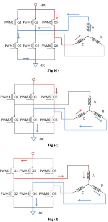
Fig (c) Table 1. Sequence for rotating motor in clockwise direction
Hall Sensor Code Phase Sequence Driver Transistor Activating sequence Phase Current
A B C A B C
0 0 1 1 Q1(PWM1) Q6(PWM6) +DC OFF -DC
0 1 0 3 Q3(PWM3) Q2(PWM2) -DC +DC OFF
1 1 0 4 Q5(PWM5) Q2(PWM2) -DC OFF +DC
1 0 0 5 Q5(PWM5) Q4(PWM4) OFF -DC +DC
Fig (d)
Fig (e)
Fig (f)
Fig. 2 (a-f). Winding energizing sequence with respect to the hall sensor
The current in the rotor is reversed to create a rotating or moving electric field by means of a split commutate or and brushes. On the other hand, in a BLDC motor the windings are on the stator and the rotor is a permanent magnet. Hence the term inside-out DC motor. To make the rotor turn, there must be a rotating electric field. Typically a three-phase BLDC motor has three stator phases that are excited two at a time to create a rotating electric field (fig 2(a-f)). This method is fairly easy to implement, but to prevent the permanent magnet rotor from getting locked with the stator; the excitation on the stator must be sequenced in a specific manner while knowing the exact position of the rotor magnets. Position information can be gotten by either a shaft encoder or, more often, by Hall Effect sensors that detect the rotor magnet position. For a
typical three phase, sensored BLDC motor there are six distinct regions or sectors in which two specific windings are excited. These are as shown in Figure 3.
DSP Processor
The dsPIC30F4011 is a 40-pin 16-bit MCU specifically designed for embedded motor control applications. AC Induction Motors (ACIM), Brushless DC (BLDC) and DC are some typical motor types for which the dsPIC30F4011 has been specifically designed. Some of the key features on the dsPIC30F4011 are (Data Sheet, 2005)
6 independent or 3 complementary pairs of dedicated
Motor control PWM outputs.
9 input, 500 kbps, ADC with up to 4 simultaneous
sampling capabilities.
Multiple serial communications: UART, I2CTMAND SPI
DSP engine for fast response in control loops.
In this application we discuss how the dsPIC30F4011 used to control a sensored BLDC motor. Hall sensor is connected to dsPIC30F4011. By reading the Hall Effect sensors, a 3-bit code can be obtained with values ranging from 1 to 6. Each codevalue represents a sector on which the rotor is presently located. Each code value, therefore, gives us information on which windings need to be excited. Thus a simple lookup table can be used by the program to determine which two specific windings to excite and, thus, turn the rotor.
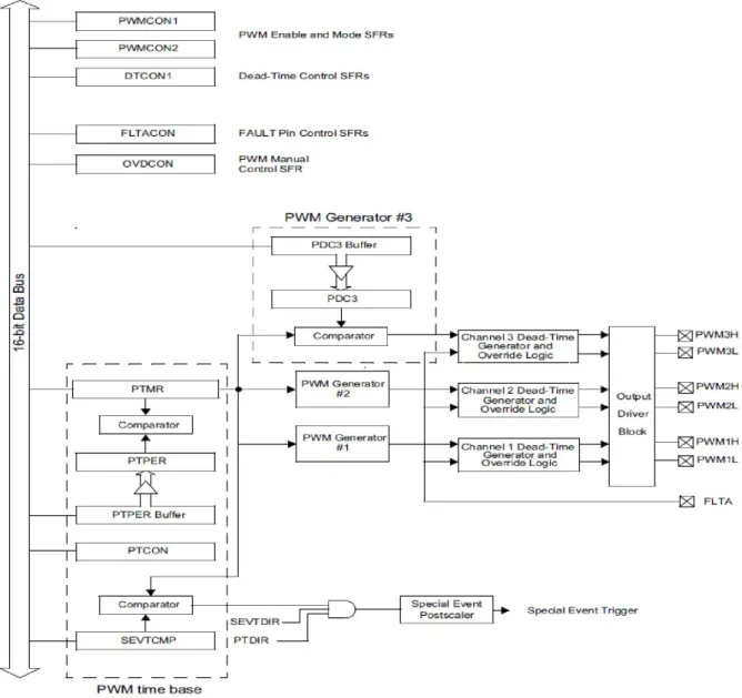
PWM CONTROL SYSTEM
Fig.4 shows the MCPWM has a dedicated 16-bit PTMR time base register. This timer is incremented by a user defined clock tick, which can be as low as TCY. The user also decides the period required for the PWM by selecting a value and loading it in the PTPER registers. The PTMR is compared to the PTPER value at every TCY. When there is a match, a new period is started. The duty cycle is controlled similarly, by loading a value in the three duty cycle registers (Stan D’Souza, 2004).
Unlike the period compare, the value in the duty cycle register is compared at every TCY/2 interval (i.e., twice as fast as the period compare). If there is a match between the PTMR value and the PDCx value, then the corresponding duty cycle output is driven low or high as dictated by the PWM mode selected.
The three outputs from the duty cycle compare are channeled to a complementary output pair where one output is high while the other is low, and vice versa. The two outputs can also be configured as independent outputs. When driven as
complementary outputs, a dead time can be inserted between the time the high level goes low and the low level goes high. This dead time is hardware configured and has a minimum value of TCY. Dead time insertion prevents inadvertent shoot-thru in output drivers. There are several modes in which the MCPWM module can be configured. Edge aligned output is probably the most common mode. The operation of an edge aligned PWM. At the start of the period, the outputs are all driven high. As the PTMR increments, a match with the duty cycle registers causes the corresponding duty cycle output to
is driven by a PWM signal (when set to 1) or (when set to 0) driven Active/Inactive by the corresponding bit field in the low byte portion of the OVDCON register. This feature allows the user to have PWM signals available, but not driving, at all output stages of the pins. For BLDC motors, the same value is written to all PDCx registers. Depending on the value in the OVDCON register, the user can select which pin gets the PWM signal and which pin is driven active or inactive. When controlling the BLDC sensored motor it is necessary to excite two winding pairs depending on where the rotor is located and dictated by the value of the hall sensors. In the CN Interrupt service routine the hall sensors are read and then the value of the sensors is used as an offset in a lookup table which corresponds to the value which will be loaded in the OVDCON register
OPTO-Coupler Interface
An opto-coupler is a solid-state component in which the light emitter, the light path and the light detector are all enclosed within the component and cannot be changed externally. As the opto-coupler provides the electrical isolation between circuits, it is called opto-isolator. An opto-coupler allows signal transfer without coupling wires, capacitors or transformers as shown in fig.5
Fig. 5. Interfacing of opto-coupler
Power circuit of motor
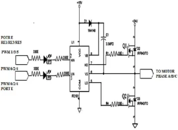
Fig. 6. MOSFET Bridge Schematic
A 3-phase full bridge arrangement was chosen for the power interface between the motor and controller. The full bridge was chosen for it higher torque output capability over a half bridge arrangement. The purpose of the bridge circuit is to enable each of the three motor phases to be switched on as
required by the motor truth table. Due to the large currents each MOSFET has flowing through it, the potential exists to have very large power dissipation through the device. Figure 6 shows the connection of the three-phase transistor (Robert, 2005).
Fig. 7Gate Drive Schematic
To provide reliable operation, the transistors in the three-phase bridge had to meet certain specifications. The new 200V automotive standard dictated that MOSFETs be capable of 24-volt operation. They also had to have low drain-source resistance to minimize conduction losses. In this project load current is 5A. So continuous current is 2*5A, that is 10A continuous current through MOSFET. Peak current through MOSFET is 10*5A, that is 50A. To achieve these requirements, a new 24-volt automotive MOSFET from International Rectifier, the IRF640 was chosen. The gate driver chosen for the design was an International Rectifier IR2101. It has in a single 8-pin package both a high and low side gate driver. As such, one IR2101 is capable of driving one MOSFET pair. Since the motor controller is intended for a three-phase motor, there are three identical gate driver circuits. From figure 8, U1 is the IR2101 gate driver; diode D1 and capacitor C1 form the bootstrapping arrangement for the high side gate driver as shown in Fig.7.
Hall Effect sensor interface
Most brushless DC motors have incorporated in the stator several Hall Effect sensors. These sensors provide rotor position information to the motor controller. Hall sensors are connected to port B. It is input port because it gives information of motor position.
Hall Effect sensors are open collector devices as shown in Figure 8.The 3-Phase BLDC Motor Control Drive contains a hall-effect interface. The circuit is designed to accept +5 V to +15.0 V encoder or hall-effect sensor inputs. Input noise filtering is supplied on the input path for the encoder/hall-effect interface.
sensors by limiting current, 10kΩ pull up resistors are used. To limit current 1KΩ resistors are connect in series with Hall sensors.
Fig. 8. Hall Effect Sensor
Closed loop Control
As system make SWITCH ON .It initialize MCPWM, ADC, Timers & Ports. System reads hall sensor signals and read last set speed. Set speed stored in the period registers PDC1, PDC2, and PDC3. As START Key is pressed. According to hall sensor signal read lookup table, Load the OVDCON register and ON the PWM signals and motor starts to rotate. As STOP key is pressed. DSP processer disables PWM signals. This closed loop system explains in following
flowchart. Fig. 9. Flow chart of closed loop control
Fig. 10(a). Waveform of PWM at speed 400 rpm
These PWM signals are shown in fig 10(a), 10(b) for speed range 400rpm, & 1000rpm respectively. From waveforms it is seen that as speed increased time period of pulses decreased. From waveform it is seen that as speed increased the number of pulses are increased and time period of pulses decreased.
Brake test on BLDC motor
Brake Test method represented in figure 11 is also called as poney brake method. A rope or a belt is used to provide a brake to the motor.
To Spring balances F1 and F2 are attached to the two ends
of the rope which are kept horizontal distance equal to diameter of pulley and twice the thickness of rope.
A tension on the belt ia adjusted by adding weight F1 in fig
11.
The resistance to motion of the pulley is due to friction of
rope .The effective force acting at the rim of the pulley is (F1-F2) in kg as F1 opposes motion and F2 helps motion
Therefore torque T developed by the motor is equal to (F1-F2)*effective radius of pulley
Fig. 11. Break test method
Output Power of motor=2πNTmkg/sec
60 Where, T=(F1-F2) * r Or
Output Power of motor=2πNT*9.81
60 watts
The Input the motor is measured by a voltmeter and
ammeter connected in the motor line i.e.,
Input Power =VL*IL Watts
η % of motor = 2πNT * 9.81*100
60* VL*IL
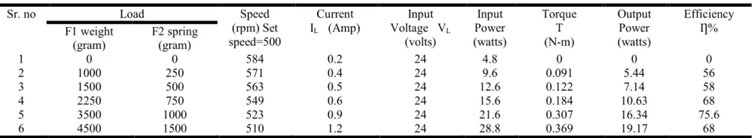
Through brake test current, voltage& speed are measured. From these observations output power, Torque & efficiency are calculated In this project diameter of pulley is 2.5 cm
Conclusion
This paper presents a review based on application on different control strategies using different controllers for the speed control of BLDC motors. Here the first controller is superior and reduces cost and easily realized for industrial application for simple algorithm. In a digital control system specialized hardware peripherals provide efficient motor control with limited support circuitry, reducing the cost and complexity of the motor control hardware. In genetic base control the load torque disturbance applied to the BLDC motor operation, the rotor speed can be regulated to operate within ±5% speed error band.
REFERENCES
“dsPIC30F4011/4012” Data Sheet, High Performance Digital Signal Controllers, 2005 Microchip Technology Inc. Datasheet of IRF640, Vishay Siliconix,2011
HCPL-817 Datasheet, AVAGO Technologies. IR2101 Datahseet,. International Recifier, 2003.
Padmaraja Yedamale, 2003. Microchip Technology Inc.
AN885 - Brushless DC (BLDC) Motor Fundamentals, ã 2003 Microchip Technology Inc.
PadmarajaYedamale, 2004. Microchip Technology Inc.AN899
- Brushless DC MotorControl Using PIC18FXX31 MCUs Microchip Technology Inc.
Robert, L,. Boylestad, Louis Nashelsky,” Electronic Devices And circuit Theory”, Prentice-Hall India
Stan D’Souza, 2004. Microchip Technology, AN957 - Sensored BLDC Motor Control Using dsPIC30F 2010, Microchip Technology Inc.
Observation Table
Table 8.6. Observation table of load test
Sr. no Load Speed
(rpm) Set speed=500
Current
IL (Amp)
Input Voltage VL
(volts) Input Power (watts) Torque T (N-m) Output Power (watts) Efficiency Ƞ% F1 weight (gram) F2 spring (gram)
1 0 0 584 0.2 24 4.8 0 0 0
2 1000 250 571 0.4 24 9.6 0.091 5.44 56
3 1500 500 563 0.5 24 12.6 0.122 7.14 58
4 2250 750 549 0.6 24 15.6 0.184 10.63 68
5 3500 1000 523 0.9 24 21.6 0.307 16.34 75.6
6 4500 1500 510 1.2 24 28.8 0.369 19.17 68