http://dx.doi.org/10.4236/jemaa.2013.512063
A Novel Adjustable Plasmonic Filter Realization by Split
Mode Ring Resonators
Mohsen Janipour, Mohammad Azim Karami, Rahman Sofiani, Farrokh Hodjat Kashani
Department of Electrical Engineering, Iran University of Science and Technology, Tehran, Iran. Email: [email protected]
Received September 4th, 2013; revised October 7th, 2013; accepted November 5th, 2013
Copyright © 2013 Mohsen Janipour et al. This is an open access article distributed under the Creative Commons Attribution License, which permits unrestricted use, distribution, and reproduction in any medium, provided the original work is properly cited. In accor-dance of the Creative Commons Attribution License all Copyrights © 2013 are reserved for SCIRP and the owner of the intellectual property Mohsen Janipour et al. All Copyright © 2013 are guarded by law and by SCIRP as a guardian.
ABSTRACT
A novel nanoscale plasmonic filter consisting of two coupled metal-insulator-metal (MIM) waveguides is introduced. The new structure functionality is verified by numerical simulations in different configurations of the filter. The im-pedance variation characteristic named as split mode ring resonancy is achieved by partially narrowing or expanding the waveguide diameter. The main parameters of the filter are evaluated by using the parameters of an implemented type of ring resonator. Moreover, modal analysis for Surface Plasmon Polariton (SPP) propagation is performed while changing the main spatial parameters of the device.
Keywords: Plasmonic Filter; Ring Resonator; MIM Waveguide
1. Introduction
Plasmonics and integrated optical devices play an im-portant role in routing, switching and controlling of light in the various fields of modern optical communication and networks [1]. Plasmonic waveguides transfer the electromagnetic waves coupled to surface collective os-cillations of free electrons on a metal, called Surface Plasmon Polaritons (SPPs). The SPP waves are bound to and propagate along metal-dielectric-metal interfaces [2]. The light confinement below the diffraction limit is the main identity of plasmonic waveguide making them dif-ferent from other types of optical waveguides such as photonic crystals, optical fibers, etc. Furthermore, the introduction of deep-submicron technologies in elec- tronic engineering leads to a revolution in optoelectronic circuits [3]. Various structures such as nano-particle plas- mon waveguides [4-6], Domino plasmon waveguide [7], grooves and wedges [8-10] and Metal-Insulator-Metal waveguides (MIM) [11,12], are introduced by transport- ing SPPs. In addition to the fabrication simplicity, high degree of SPP confinement and compact size have made MIM geometry the most attractive among other nano- sclae waveguides [13]. Different types of plasmonic fil- ters such as tooth shaped subwavelength, and add-drop topologies are introduced and analyzed by numerical
The introduced structures suffer from some limitations such as huge dimension for splitting functionality [21,22, 24], insulation lack between output ports [23], low trans- mittance [21-24], power leakage [21-23], and maximum fanout of two for splitter channels [21-24]. An annular ring being able to support multi-modes, should gratify the boundary conditions. Coupling and perturbation me- thods are used for the resonant mode excitation [23].
In this paper, a novel nanoscale plasmonic filter is in-troduced while its functionality is verified by numerical simulations in different configurations. Next section de-scribes the dispersion relation for the introduced filter. While the theoretical model is presented in Section 3, Section 4 describes the transmission spectrum results.
[image:2.595.311.541.88.223.2] [image:2.595.96.250.409.488.2]2. Dispersion Relation and Effective
Refractive Index of MIM Waveguides
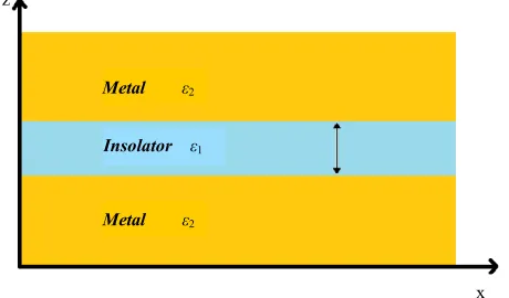
Figure 1 shows a MIM waveguide, where each metal/ dielectric interface allows SPPs with a TM mode to propagate along x direction. It is shown that whenever the separating space between two interfaces is compara-ble to the decay lengths of SPPs in the dielectric region, the SPPs get coupled to each other and confined in the dielectric region between two metals [1]. The field analy-sis inside the dielectric space between two metals could be achieved using Maxwell’s equations:1 1
1e ek z 2e e k z dielec i x i x y
H C C
1
1 2
0 1 0 1
e ek z e e k z
dielec i x i x z
C C
E
1
1
1 1 1 2
0 1 0 1
e ek z e e k z
dielec i x i x
x
ik C ik C
E
1
in which β is the propagation constant of the MIM waveguide and 2 2
1
k k0 is the wave vector nor- mal to the propagation direction and k0 is the propagation constant of free space. Using boundary conditions and the field components in the metal region, the dispersion relation of MIM waveguide structure could be calculated by:
2 2 2 1
0 2 2
2 0 tanh 2 k h k k
where indices 1 and 2 denote the dielectric and metal layers, respectively. Silver is regarded as the metal in this paper, and Drude-Lorentz model with five poles is used for dielectric constant determination [25]:
2
5 21 2 2
1
1 p n n
n n n
f i i
where ωp = 2002.6 THz is the plasma frequency and γ =
Metal ε2
Insolator ε1
Metal ε2 z
x Figure 1. Schematic representation of an MIM structure with two semi-infinite metal slabs of permittivity ε2 sur- rounding a dielectric layer of thickness h and permittivity
ε1.
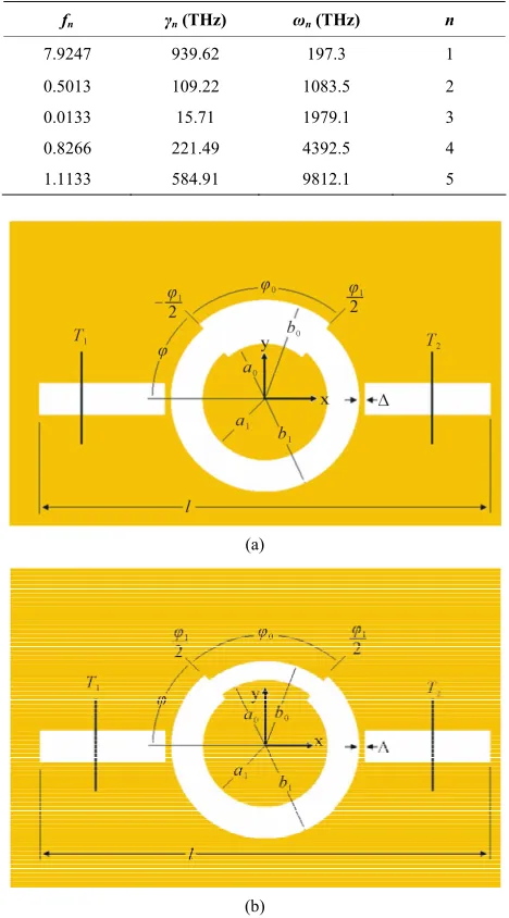
11.6012 THz is the damping constant. Table 1 summa- rizes the main values for dielectric constant calculation, i.e.ωn resonant frequencies of silver, damping constants γn , and oscillator strength fn [25].
3. Theoretical Model
The Local Split Resonant (LSR) mode of a circular ring resonator and its effects on the transmission spectra is investigated in this paper theoretically and numerically.
Figure 2 presents the LSR mode excitation using dif-ferent impedances on the ring resonator. The coupling separation distance Δ is 10 nm and the device length l is set to 1 µm.
The input and output MIM waveguides are coupled by means of a LSR ring resonator made out of two sectors with different impedances. Sector (I) with inside and outside radius of a0 and b0, and r0 as the average
0 0 0 2
r a b , has a higher characteristic impedance in compare with sector (II) with inside, outside and av-erage radius as ai, bi and ri
aibi
2, respectively.Solving the wave equation in cylindrical coordinates, field distribution in region (I) can be written as:
0 , ,
, , sin
I I I
z n o n
I I
n o n
E E J k a Y k J k a Y k
0
I I
I j r Ez
H
0 I
I I z
r E H j
where, pπ0 for –π 20π 2, and n is the
nth roots of Bessel functions of the ξth order which has infinite discrete roots, and ir
I r a
Table 1. Silver values for evaluating Drude-Lorentz model.
fn γn(THz) ωn(THz) n
7.9247 939.62 197.3 1
0.5013 109.22 1083.5 2 0.0133 15.71 1979.1 3 0.8266 221.49 4392.5 4 1.1133 584.91 9812.1 5
(a)
(b)
Figure 2. (a) Schematic of the split mode circular ring re-sonator with an increasing sector between −φ0/2and φ0/2, (b) Schematic of the split mode circular ring resonator with a decreasing sector between −φ0/2andφ0/2.
field distribution for region (II) can be calculated from:
0 , ,
, , sin
II II II
z m i m
II II
m i m
E E J k a Y k
J k a Y k
0
II II II j r Ez
H
0 II
II II z
r E H j
where, v q π π
0
for π 203π 2 , and m is the mth roots of Bessel functionsof the vth order. Jv and Yv represent the first kind and second kind Bessel function of order v, respectively. Us-ing boundary condition at ρ = ai and ρ = bi in region (II), and either one ofρ = a0 orρ = b0 for region (I), one ob-tains:
1, 2,3, ,
q
0 0
i i
III II
m z r z
a a
j E j E
0 0 i i III IIm z r z
b b
j E j E
and
0 0 o o III IIm z r z
a a
j E j E
0 0 o o III IIm z r z
b b
j E j E
In addition, using the continuity of tangential compo-nents of the magnetic fields at φ = φ0/2 and φ = φ0/2, it can be found that
, 0 , 0
2 2
I II
o i
H r H r
, 0 , 0
2 2
I II
o i
H r H r
In conclusion, the characteristic equation is obtained being useful for mode calculation in sector (I).
, , , , I Im o m o
I I
m o m o
J k b Y k b J k a Y k a
Similarly, characteristic equation for sector (II) can be found as:
, , , , II IIn i n i
II II
n i n i
J k b Y k b J k a Y k a
It should be noted that n = 0 and m = 0 are not ac-ceptable for all of these equations because of existence of second order Bessel functions in the equations. In fact, each of these sectors follows its individual characteristic equation to illustrate encompass modes in any wave-length. However, instead of using TMv.m and TMξ.n for each sector, it is preferred to use one notation to specify modes of the whole ring structure which is made of two sectors with different radial widths. Hence, in this study
, .
n v m
[image:3.595.310.515.151.300.2]one of these modes does not exist, we cannot use this notation and it is essential to use another one. For exam-ple, in this study, if there is no propagating mode inside region (II) or region (I), .
I n
TM and . II v m
TM , are only used respectively. However, it should be noted that, these resonant modes build a local resonance inside the ma-nipulated sectors and other resonant modes which cannot satisfy the local resonant condition, are lost due to scat-tering inside the manipulated regions. For example, con-sidering φ0 = π/6, it is anticipated that only the ξ = 6p (integer multiples of sixth) mode maintains the resonant condition and other modes split.
4. Plasmonic Filter with a LSR Circular
Ring Resonator
[image:4.595.310.535.86.400.2]4.1. Typical Band-Pass Filter with a Circular Ring Resonator
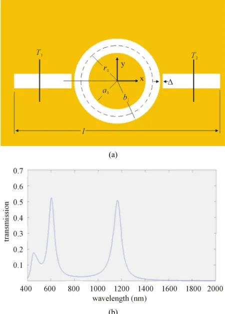
Figure 3 shows a typical plasmonic band-pass filter by the means of a circular ring resonator consisted of two MIM waveguides coupled together by a circular ring resonator [14]. The main parameters are Δ, a, b, r and h describing the coupling separation and the ring resonator, inside, outside and the average radius of the ring resona-tor, and the MIM waveguides width, respectively. In this investigation, in order to have fundamental mode (TM0),
h is considered to be 50 nm; to achieve a definitive sub- wavelength structure. In such structures it is essential to monitor the input signal (T1), the output signal (T2), ana-lyzing the power in the frequency domain to reach trans-mission coefficient, defined as output power divided into input power, T = Pout/Pin. Figure 3 shows the transmis-sion spectrum of a typical circular ring resonator with Δ = 10 nm, a = 100 nm, b = 150 nm as the main property of the filter.
The filter is placed in a length of L = 1 µm. It can be seen from Figure 3(b) that there exist two resonant peaks, related to two different resonant modes with the wave-lengths of λ1 = 1162 nm for the first mode, and λ2 = 602 nm for the second mode. Considering ri and ro as the inside and outside radius of the ring resonator, respec-tively, it is shown that these modes can be computed us-ing the followus-ing equation [23]:
0n o i
n o i
J kr r
Y kr
n n J k Y kr
in which k c
r r
is the wave number,
0 0
1
c , εr and μr are light speed in free space, relative permittivity and permeability, respectively. It can be shown that the effective refraction index of a MIM structure can be computed as [1]:
0 0
Re Im
Re eff Im
eff eff
i
n n i n
k k
(a)
(b)
Figure 3. (a) Schematic of a typical plasmonic MIM band- pass filter using a circular ring resonator, (b) The transmis-sion spectrum of a typical plasmonic MIM band-pass filter using a circular ring resonator.
The transmission simulation of the filter is calculated using 2D FDTD and is shown in Figure 3(b). In these simulations, it is assumed that the size of each uniform Yee cell of the structure in x and z-directions are Δx = Δz = 2 nm. The computation domain of this structure is a conventional perfectly matched layer (CPML) absorbing boundary condition.
4.2. Adjustable Plasmonic Filter Using a Split Mode Ring Resonator
This section investigates the effect of using a split mode ring resonator on the main modal characteristics. In fact, the split mode resonator is made out of two or more changed impedance circular sectors on the circular ring. Due to impedance changing, a local resonant boundary condition is created which can reserve or split the differ-ent mode’s energy. It is assumed for simplicity that the constant coupling distance Δ, was setting as that in the investigated structure (see Figure 2).
(a)
(b)
(d)
Figure 4. (a) The transmission spectrum of the split mode ring resonator plasmonic filter for even values of m in an decreas-ing split sector with a0 = 110 nm, b0 = 140nm, constant φ0 = π/3 and alternating φ1, (b) The transmission spectrum of the split mode ring resonator plasmonic filter for odd values of m in an decreasing split sector with a0 = 110 nm, b0 = 140 nm, constant
φ0 = π/3 and alternating φ1, (c) The transmission spectrum of the split mode ring resonator plasmonic filter for some odd val-ues of m in an increasing split sector with a0 = 90 nm, b0 = 160 nm, constant φ0 = π/3 and alternating φ1, (d) The transmission spectrum of the split mode ring resonator plasmonic filter for even values of m in an increasing split sector with a0 = 90 nm, b0 = 160 nm,constant φ0 = π/3 and alternatingφ1.
constant and φ1 is varying relative to the x-axis, as the port’s main axis. In this study in order to investigate the manipulated position dependency of the sector, it is as-sumed that φ1 = mπ/12, . Figure 4(c) shows that in the expanded sector case (for example a0 = 90 nm and b0 = 160 nm) and for odd m numbers, the transmission spectrum amplitude for all modes are in-creased by approaching φ1 to 5π/12. In addition, this fig-ure shows that for the sector which is placed nearby the ports, the first mode disappears and two new resonant modes are created in return and a valley appears. The valleys become deeper by decreasing the distance of sec-tor expansion to the ports.
1, 2,3,
m
The effect of even m numbers is shown in Figure 4(d). It is obvious that by approaching the manipulated sector to the ports, each of the original first and second resonant modes split into two new lateral resonant modes. In addi-tion, the transmission spectrum for m = 5 is shown in
Figures 4(c) and (d) to demonstrate the transmission spectrum when φ1 gets close to 5π/12for which, the ma-nipulated sector is homolographic around y axis. In other words, the influence of increasing m on the transmission spectrum is a periodic process. Hence, it is essential to analyze the transmission spectrum using even/odd m.
As the center of the sector approaches π/2, the trans-mission amplitude of the first mode of the splitted modes increases and the amplitude of the second mode de-creases gradually. Finally, for m = 5, for which the sector
is symmetric around y axis, the transmission amplitude takes a resonant peak which is the mean value of the neighboring amplitudes. Figure 4(b) illustrates the effect of odd m values on the transmission spectrum. It is ob-vious that, splitting is occurred and a large increase of the transmission amplitude is observed for the second reso-nant mode and for all m values. However, splitting phe-nomena affects the second resonant mode less severe in comparison with the first mode. In addition, according to
Figure 4(b), it is found that, unlike previous discussion for even values of m, the augmenting of φ1 will not end in the enhancement of second mode transmission ampli-tude. Alternating the width of the manipulated sector could play an important role on transmission spectrum.
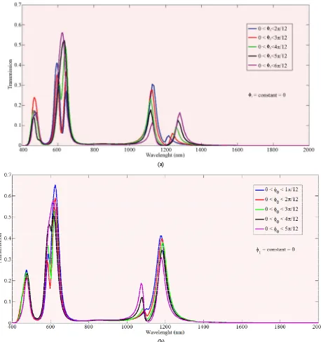
Figure 5 depicts the transmission spectrum, affected by changing φ0of manipulated sector, respectively. In order to study the effects of changing φ0 on transmission spec-trum, first we consider the narrowing sector case with a0 = 110 nm, b0 = 140 nm andφ1 = 0 and then we investi-gate the effect of changing φ0. Moreover, this effect is investigated for the case that the sector is symmetric around y axis. According to Figure 5(a), the second reso-nant mode of a typical ring resonator is splitted into two different resonant peaks. By enhancing φ0 from 2π/12 to
[image:6.595.96.499.83.308.2](a)
(b)
Figure 5. (a) The transmission spectrum of the split mode ring resonator plasmonic filter with φ1 constant and changing φ0 for decreasing sector, (b) The transmission spectrum of the split mode ring resonator plasmonic filter with φ1 constant and
changing φ0 for increasing sector.
results in reducing the amplitude of the first resonance and generating a new quasi-first order resonant mode with a less amplitude in compare with the previous one.
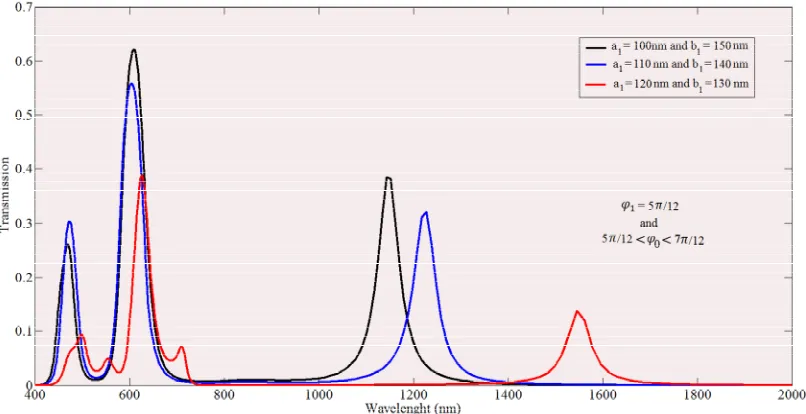
Another parameter which affects the operation of a split ring resonator is the changing of the radial width of the manipulated sector. Figure 6 depict the transmission spectrum in the case that the radial width of the manipu-lated sector takes different values.
It is concluded from Figure 6 that augmenting the
ra-dial width of the enhanced sector will end in a red shift for the second resonance, which is a significant property of integrated nano-optic circuits. In other words, using a sector with a small expanded radial width with angular width of π/6 and φ1 = 5π/12, it is possible to reach higher resonant wavelengths (or more size reduced circuits) without the whole structure scaling.
[image:7.595.68.526.84.572.2]
Figure 6. The transmission spectrum of a split mode ring resonator for an increased sector with φ1 = 5π/12and 5π/12 < φ0 < 7π/12, and varying a0 and b0.
Figure 7. (a) The Real (Hy) field profile of the decreased split mode ring resonator ofφ0 = π/6,φ1 = 5π/12, a0 = 110 nm and b0 = 140 nm for λ = 476.5 nm, (b)λ = 608.3 nm, (c)λ = 1228 nm.
wavelengths.
5. Conclusion
[image:8.595.311.533.333.542.2]location, and the manipulation thickness.
6. Acknowledgements
The authors would like to thank Iranian Nanotechnology Initiative Councilman and Professor Ali Beitollahi for their support.
REFERENCES
[1] S. I. Bozhevolnyi, “Plasmonic Nanoguides and Circuits,” In: S. I. Bozhevolnyi, Ed., Plasmonics and Metamaterials, Pan Stanford Publishing, Singapore City, 2008.
http://dx.doi.org/10.1142/9789814241335
[2] H. Raether, “Surface Plasmon Smooth and Rough Sur- faces and on Gratings,” Springer-Verlag, Berlin, 1988. [3] E. Ozbay, “Plasmonics: Merging Photonics and Electron-
ics at Nanoscale Dimensions,” Science, Vol. 311, No. 5758, 2006, pp. 189-193.
http://dx.doi.org/10.1126/science.1114849
[4] S. A. Maier, P. G. Kik, H. A. Atwater, S. Meltzer, E. Harel, B. E. Koel and A. G. Requicha, “Local Detection of Electromagnetic Energy Transport below the Diffrac- tion Limit in Metal Nanoparticle Plasmon Waveguides,” Nature, Vol. 2, No. 4, 2003, pp. 229-232.
http://dx.doi.org/10.1038/nmat852
[5] M. Quinten, A. Leitner, J. R. Krenn and F. R. Aussenegg, “Electromagnetic Energy Transport via Linear Chains of Silver Nanoparticles,” Optics Letters, Vol. 23, No. 17, 1998, pp. 1331-1333.
http://dx.doi.org/10.1364/OL.23.001331
[6] S. A. Maier, P. G. Kik and H. A. Atwater, “Optical Pulse Propagation in Metal Nanoparticle Chain Waveguides,” Physical Review B, Vol. 67, No. 20, 2003, Article ID: 205402. http://dx.doi.org/10.1103/PhysRevB.67.205402 [7] D. Martin-Cano, M. L. Nesterov, A. I. Fernandez-Do-
minguez, F. J. Garcia-Vidal, L. Martin-Moreno and Este- ban Moreno, “Domino Plasmons for Sub Wavelength Terahertz Circuitry,” Optics Express, Vol. 18, No. 1, 2010, pp. 754-764.
http://dx.doi.org/10.1364/OE.18.000754
[8] D. F. P. Pile and D. K. Gramotev, “Channel Plasmon-Po- lariton in a Triangular Groove on a Metal Surface,” Op- tics Express, Vol. 29, No. 10, 2004, pp. 1069-1071. http://dx.doi.org/10.1364/OL.29.001069
[9] S. I. Bozhevolnyi, V. S. Volkov, E. Devaux and T. W. Ebbesen, “Channel Plasmon-Polariton Guiding by Sub- Wavelength Metal Grooves,” Physical Review Letters, Vol. 95, No. 4, 2005, Article ID: 046802.
http://dx.doi.org/10.1103/PhysRevLett.95.046802 [10] D. K. Gramotev and D. F. P. Pile, “Single-Mode Sub-
Wavelength Waveguide with Channel Plasmon-Polari- tons in Triangular,” Applied Physics Letters, Vol. 85, 2004, pp. 6323-6325.
http://dx.doi.org/10.1063/1.1839283
[11] E. Verhagen, J. A. Dionne, L. Kuipers, H. A. Atwater and A. Polman, “Near-Field Visualization of Strongly Confin- ed Surface Plasmon-Polaritons in Metal-Insulator-Metal
Waveguides,” NanoLetters, Vol. 8, No. 9, 2008, pp. 2925-2929. http://dx.doi.org/10.1021/nl801781g
[12] J. A. Dionne, L. A. Sweatlock, H. A. Atwater and A. Polman, “Plasmon Slot Waveguides: Towards Chip-Scale Propagation with Subwavelength-Scale Localization,” Physical Review B, Vol. 73, No. 3, 2006, Article ID: 035407. http://dx.doi.org/10.1103/PhysRevB.73.035407 [13] Y. Matsuzaki, T. Okamoto, M. Haraguchi, M. Fukui and
M. Nakagaki, “Characteristics of Gap Plasmon Wave- guide with Stub Structures,” Optics Express, Vol. 16, No. 21, 2008, pp. 16314-16325.
http://dx.doi.org/10.1364/OE.16.016314
[14] T. B. Wang, X. W. Wen, C. P. Yin and H. Z. Wang, “The Transmission Characteristics of Surface Plasmon Polari- tons in Ring Resonator,” Optics Express, Vol. 17, No. 26, 2009, pp. 24096-24101.
http://dx.doi.org/10.1364/OE.17.024096
[15] X. Lin and X. Huang, “Tooth-Shaped Plasmonic Wave- guide Filter with Nanometric Sizes,” Optics Express, Vol. 33, No. 23, 2008, pp. 2874-2876.
http://dx.doi.org/10.1364/OL.33.002874
[16] J. Tao, X. G. Huang, X. Lin, Q. Zhang and X. Jin, “A Narrow-Band Subwavelength Plasmonic Waveguide Filt- er with Asymmetrical Multiple Teeth-Shaped Structure,” Optics Express, Vol. 17, No. 16, 2009, pp. 13989-13994. http://dx.doi.org/10.1364/OE.17.013989
[17] P. H. Lee and Y. C. Lan, “Plasmonic Waveguide Filters Based on Tunneling and Cavity Effects,” Springer, Vol. 5, 2010, pp. 417-422.
[18] A. Setayesh, S. R. Mirnaziry and M. S. Abrishamian, “Nu-Merical Investigation of Tunable Band-Pass\Band- Stop Plasmonic Filters with Hollow-Core Circular Ring Resonator,” Optical Society of Korea, Vol. 15, No. 1, 2011, pp. 82-89.
http://dx.doi.org/10.3807/JOSK.2011.15.1.082
[19] A. Hosseini and Y. Massoud, “Nanoscale Surface Plas- mon Based Resonator Using Rectangular Geometry,” Ap- plied Physical Letters, Vol. 90, No. 18, 2007, Article ID: 181102. http://dx.doi.org/10.1063/1.2734380
[20] A. V. Krasavin and A. V. Zayats, “Electro-Optic Switch- ing Element for Dielectric-Loaded Surface Plasmon Po- lariton Waveguides,” Applied Physical Letters, Vol. 96, No. 4, 2010, Article ID: 041107.
http://dx.doi.org/10.1063/1.3464552
[21] Q. Li, T. Wang, Y. Su, M. Yan and M. Qiu, “Coupled Mode Theory Analysis of Mode-Splitting in Coupled Ca- vity System,” Optics Express, Vol. 18, No. 8, 2010, pp. 8367-8382. http://dx.doi.org/10.1364/OE.18.008367 [22] H. Lu, X. Liu, D. Mao, L. Wang and Y. Gong, “Tunable
Band-Pass Plasmonic Waveguide Filters with Nanodisk Resonators,” Optics Express, Vol. 18, No. 17, 2010, pp. 17922-17927. http://dx.doi.org/10.1364/OE.18.017922 [23] I. Wolff and N. Knoppik, “Microstrip Ring Resonator and
Dispersion Measurement on Microstrip Lines,” Electron- ics Letters, Vol. 7, No. 26, 1971, pp. 779-781.
http://dx.doi.org/10.1049/el:19710532
Artech House, Norwood, 2005.
[25] A. Pannipitiya, I. D. Rukhlenko, M. Haroldo, T. Hattori and G. P. Agrawal, “Improved Transmission Model for