1
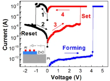
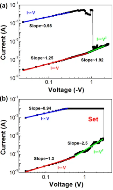
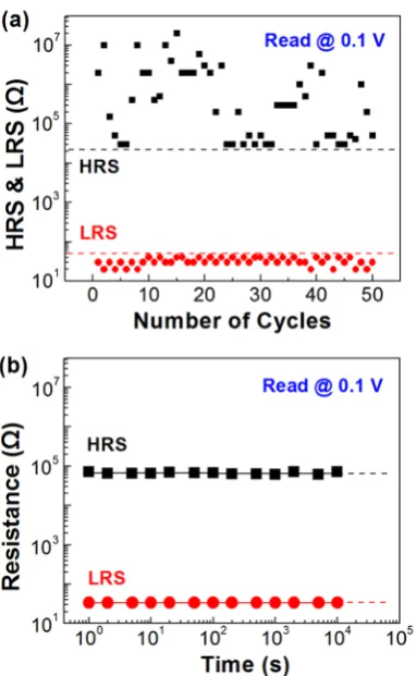
Bipolar resistive switching characteristics of low temperature grown ZnO thin
1films by plasma-enhanced atomic layer deposition
23
Jian Zhang,1) Hui Yang,1) Qi-long Zhang,1, a) Shurong Dong,2, a) J.K.Luo2, 3)
4 5
1
Department of Materials Science and Engineering, Zhejiang University, Hangzhou 310027,
6
China
7
2
Department of Information Science and Electronic Engineering, Zhejiang University,
8
Hangzhou 310027, China
9
3
Institute of Renewable Energy & Environmental Technology, Bolton University, Deane
10
Road, Bolton, BL3 5AB, UK
11 12 13
ZnO films deposited by plasma-enhanced atomic layer deposition (PEALD) have
14
been used to investigate resistive memory behavior. The bipolar resistance switching
15
properties were observed in the Al/PEALD-ZnO/Pt devices. The resistance ratio for
16
the high and low resistance states (HRS/LRS) is more than 103, better than that of
17
other ZnO devices deposited by other methods. The dominant conduction mechanisms
18
of HRS and LRS are trap-controlled space charge limited current and Ohmic behavior,
19
respectively. The resistive switching behavior is induced upon the
20
formation/disruption of conducting filaments. This study demonstrated that the
21
PEALD-ZnO films have better properties for the application in 3D resistance random
22
access memory.
23 24 25 26
Bipolar resistive switching (BRS) behaviors in transition-metal oxides (TMO) has been
27
intensively studied as the next generation nonvolatile resistance random access memory
28
(ReRAM).1,2 The BRS behavior originates from the repeated resistance change between the high
29
resistance state (HRS) and low resistance state (LRS), and is controlled by electric field with
30
a
2
opposite polarity.3 The resistive switching behaviors were observed from various binary TMO
1
thin films such as NiO, TiO2, ZnO and others.4-6 This type of memory devices, generally
2
composed of metal-insulator-metal structures, have many merits for applications such as
3
high-density, high-speed and low-power consumption.
4
Owing to its direct energy band gap and abundance of the raw material, ZnO is an important
5
material, ideally suited for applications in optoelectronics and electronics. Recent researches
6
have shown that ZnO-based thin films have good resistive switching characteristics as well and
7
are very promising for ReRAM application. BRS characteristics have been observed in
8
TiN/ZnO/Pt, Ag/ZnO/Pt, Cr/ZnO/Pt, Al/ZnO/Pt and Al/ZnO/Si devices.6-8 Most of the ZnO
9
films were deposited by physical vapor-phase deposition (PVD) method, especially the
10
magnetron sputtering. There has been limited activity in using chemical vapor-phase deposited
11
(CVD) ZnO films to make the resistive switching devices. Atomic layer deposition (ALD), a
12
special CVD technique, has potential benefits for high quality ZnO deposition owing to precise
13
thickness controllability, large area uniformity, and low process temperature.9 ALD is much
14
better for electronic applications, especially when the films are extremely thin in nanometers
15
range. Furthermore, ALD growth has a high conformality which is particularly suitable for 3D
16
memories constructed in the cross-bar architecture.10 Therefore, it is of great interest to
17
investigate whether ZnO thin films grown by ALD can be used for ReRAM application.
18
In this paper, we report the BRS behaviors in undoped ZnO polycrystalline films deposited
19
by a remote plasma-enhanced ALD (PEALD) method. By using remote PEALD, the defects
20
associated with the plasma damage can be minimized.11 Although ZnO films can also be grown
21
by thermal ALD (THALD),12 the resistivity of THALD-grown ZnO films is typically very low
22
(<10 Ω•cm) due to high carrier concentration induced by oxygen vacancies, hence are not
23
suitable for BRS device fabrication. Whereas the resistivity of the PEALD-grown ZnO films was
24
found much higher (>104Ω•cm), and should be good for the BRS device applications.
25
The polycrystalline ZnO thin films were grown by PEALD on (111) Pt/Ti/SiO2/Si
26
substrates. Diethylzinc (DEZn, 99.9999%) precursor was used for the deposition of ZnO. The
3
carrier gas and purging medium were 99.999% purity argon. During the growth, the pressure in
1
the chamber was ~1 torr, and the substrate temperature was held at 150 °C. The flow rate of the
2
carrier gas and the oxygen was 20 sccm and 40 sccm, respectively. A typical PEALD ZnO
3
growth sequence is composed of 0.04 s of DEZn exposure, 6 s of Ar purging, 3 s of oxygen
4
plasma exposure with RF power of 500 W, and 10 s of Ar purging. The ZnO films were ~60 nm
5
thick for the devices which were grown by 250 cycles of the ALD process. X-ray diffraction
6
(XRD) and Scanning Electron Microscope (SEM) were used to evaluate the crystal structure and
7
morphology of the films. For electrical measurement, the top Al (100nm) electrode with a
8
diameter of 200 μm was deposited by thermal evaporation using a metal mask to form the
9
Al/ZnO/Pt sandwich device structure. The current–voltage (I–V) characteristics of the devices
10
were measured using a semiconductor parameter analyzer (Agilent 4155 C) at room temperature
11
in air.
12
Figure 1(a) shows the XRD spectrum of a ZnO thin film grown on the substrate. The (111)
13
peak of the Pt bottom electrode and the (002) peak of the ZnO thin film can be clearly seen,
14
indicating that the ZnO thin film has high c-axis orientation, largely attributed to the small lattice
15
mismatch between the (002) plane of the ZnO film and Pt (111) plane. Figure 1(b) shows the
16
SEM image of the cross-section of the as-fabricated ZnO/Pt/Ti/SiO2/Si structure. The ZnO film
17
has a polycrystal structure with a thickness of approximately 60 nm.
18
19
Fig. 1. (a) XRD pattern of a ZnO thin film deposited on a Pt/Ti/SiO2/Si substrate. (b) The cross-section
20
SEM image of the ZnO/Pt/Ti/SiO2/Si structure.
4
The inset of Fig. 2 shows the schematic structure of the device and the scheme for electrical
1
measurement. The DC voltage bias was applied to the top electrode (TE: Al) with the bottom
2
electrode (BE: Pt) grounded during the measurements. It was found that the freshly-made
3
devices always have a very high resistance, ~1012Ω, and the devices do not exhibit any resistive
4
switching behavior. An electroforming process is necessary to initiate the switching behavior for
5
the devices. This is because the as-deposited ZnO films have high crystal quality with low
6
density of defects, hence are high insulating. The electroforming process generates defects inside
7
the ZnO layer, mostly by the thermally assisted electromigration of oxygen ions.13 Figure 2
8
shows the typical bipolar resistive switching characteristics of the device after the forming
9
process. The voltage bias was applied in a sweeping sequence of 1→2→3→4. The voltage
10
sweeping from 0→3.5 V with a current compliance applied was used to set the device cell from
11
the HRS to the LRS, while the opposite voltage sweep of 0→-2 V, with no current compliance,
12
was used to reset the cell back to the HRS. The current compliance was set at 10 mA during the
13
forming and set process to protect the device from permanent breakdown. However, if the
14
current compliance was set to be 50 mA or higher for the forming process, the leakage current
15
became very large during the voltage sweeping, and the devices changed to the LRS
16
permanently.
17
18
Fig. 2. Typical IV characteristics of Al/ZnO/Pt device. The inset shows the schematic structure for 19
electrical measurement of Al/ZnO/Pt device. After the forming sweep (0→5V), a Reset-Set cycle is 20
displayed. The resistance state is changed from LRS to HRS above the bias of -1V (reset) and changed 21
5
1
To clarify the mechanism of bipolar resistive switching behavior, the typical I-V curve was
2
replotted in double logarithmic plot. Figures 3(a) and 3(b) show the linear fitting of the I-V curve
3
for both the negative and positive voltage sweep regions. When the device cell is switched to the
4
LRS, the curves of log (I)-log (V) are linear with gradients near the unit (I∝V), indicating that
5
the I-V at the LRS is dominated by the Ohmic Law. At the HRS, the I-V is dominated by the
6
Ohmic Law as well at low voltage region as the current and voltage are linearly correlated. But at
7
high voltage region, the gradients of the log (I)-log (V) lines are around 2, i.e. the current is
8
dependent of square of voltage applied (I∝V2). This result can be well explained by the typical
9
trap-controlled space charge limited conduction (SCLC) injection. 6, 8, 14 The dominant
10
conduction mechanisms of these devices at each voltage region are similar to the ZnO devices
11
deposited by other methods. 6, 8, 15
12
13
6 positive (b) sweeping voltage. The colorful lines show the fitting results.
1
A few mechanisms for resistive switching have been proposed with no convincing
2
evidence.** The filamentary model has been widely accepted to explain the switching behavior
3
for other ZnO-based resistive switching devices, and other TMO devices.6, 16 After the forming
4
process, defects are formed in the ZnO film. These may include oxygen vacancies, interstitial
5
atoms or other defects , but the oxygen vacancies are believed to be the most important ones. 6,
6
16, 17
The oxygen ions migrate from the ZnO layer to/near the top electrodes at ** process. The
7
oxygen vacancies are then generated in the ZnO film, forming the filament paths. Once the
8
filaments connected the bottom electrode with the top electrode, the device cell is at the LRS.
9
Whereas at the reset process, the oxygen ions near the top electrode are pushed back into the
10
ZnO layer under the electric field, and the oxygen vacancies near the top electrode partially
11
eliminated (neutralized) by reacting with the coming oxygen ions. The electrical paths (filaments)
12
are broken, and the device cell is switched to the HRS. However there exist fragmented or
13
disconnected filaments in the ZnO film even after reset due to the limited migration of the
14
oxygen ions into the film, consequently the resistance of the HRS of the devices is always much
15
lower than that of the as-made cells. Similarly, at the set process under a positive bias, the
16
oxygen ions can migrate from the film to/near the top electrode, forming the filaments inside the
17
ZnO film again. 16
18
The endurance of the devices has been tested by switching the devices between the HRS
19
and LRS for 50 cycles with the results shown in Fig. 4(a). The device cell showed a constant
20
resistance for the LRS (~30Ω) and higher than 30 kΩ (104 Ω-107 Ω) resistance for the HRS
21
during the cycling tests. The resistance ratio HRS/LRS is over 103 (103-106), which is higher than
22
the Al/PVD-ZnO/Pt devices (102-103) 6-8, implying the high quality and low defect density of the
23
ZnO films deposited by PEALD. The set voltage for our devices ranges from 1.2 to 3.6 V,
24
whereas , that for Al/PVD-ZnO/Pt devices is from 0.47 to 2. 6V, lower than those of the
25
PEALD-ZnO devices. Both the reset voltages are very low, about 0.5V. 6 Furthermore, similar
26
BRS behaviors were obtained from cell to cell on the same wafer and from different wafers,
7
showed good repeatability and uniformity. However, the HRS resistance of the devices during
1
the cycling tests varies significantly as shown in Fig. 4(a), and it is attributed to the difference in
2
the free energies of oxide formation for Al and Zn. According to the research6, the materials of
3
the top electrode have a strong influence on the resistance. The Cr/ZnO/Pt devices have a smaller
4
variation in resistances than the Al/ZnO/Pt devices shown here, and it is attributed to the smaller
5
difference in free energies of oxide formation for Cr and Zn than that of Al and Zn. During the
6
reset process, the top electrode cannot provide sufficient oxygen ions, some of the oxygen
7
vacancies are left as they are near the top electrode, resulting in different resistance for
8
each cycling test.10,11 The endurance performance of the devices is expected to be improved
9
significantly by scaling down the cell size or by improving the fabrication process.
10
11
12
Fig. 4. (a) Endurance test for 50 consecutive Reset-Set cycles, readout at 0.1 V. (b) Retention tests of 13
HRS and LRS after the Reset and Set, respectively, readout at 0.1 V. 14
8
The retention time of the Al/ZnO/Pt devices was measured at the HRS and LRS at room
1
temperature at a voltage of 0.1 V as shown in Fig. 4(b). No electrical power was needed to
2
maintain the resistances constant at the given states. Up to 104 s, the resistances of the HRS and
3
LRS show no sign of deterioration at all, implying that the information stored in the devices can
4
be kept much longer than 104 s. Therefore it can be concluded that the pure ZnO thin films
5
deposited by PEALD can meet the requirement for ReRAM device application.
6
In summary, nanocrystalline ZnO thin films were grown by PEALD technique at low
7
temperature, and were used to fabricate Al/ZnO/Pt resistive switching devices. Reversible
8
resistive switching behavior of the devices has been obtained by electrically induced resistive
9
switching between the LRS and HRS. The dominant conduction mechanisms of the LRS and
10
HRS were Ohmic behavior and trap-controlled SCLC, respectively. The resistance ratio of the
11
HRS to the LRS is larger than 103, and the resistances at both the states remain unchanged for
12
the test up to 104 s, demonstrated the excellent potential of the PEALD-ZnO films for the
13
applications in 3D ReRAM.
14
15
This work was supported by the Ministry of Science and Technology of China through the
16
National Key Technology Support Program (No.2009BAG12A07), the National Natural Science
17
Foundation of China (No. 61150110485), Zhejiang Province Innovation Group Program (No.
18
2011R09010) and Natural Science Foundation (Z1110168).
19 20 21
References
22
1R. Waser and M. Aono, Nat. Mater. 6, 833 (2007).
23
2J. J. Yang, M. D. Pickett, X. M. Li, D. Ohlberg, D. R. Stewart, and R. S. Williams, Nat. Nanotechnol. 3, 429
24
(2008). 25
3B. Magyari-Kope, M. Tendulkar, S. G. Park, H. D. Lee, and Y. Nishi, Nanotechnology 22, 25402925SI (2011).
26
4Y. S. Kim, J. S. Kim, J. S. Choi, I. R. Hwang, S. H. Hong, S. O. Kang, and B. H. Park, Appl. Phys. Lett. 98,
27
19210419 (2011). 28
5D. B. Strukov, G. S. Snider, D. R. Stewart, and R. S. Williams, Nature 453, 80 (2008).
29
6
W. Y. Chang, H. W. Huang, W. T. Wang, C. H. Hou, Y. L. Chueh, and J. H. He, J. Electrochem. Soc. 159, 29 30
9
7
J. J. Ke, Z. J. Liu, C. F. Kang, S. J. Lin, and J. H. He, Appl. Phys. Lett. 99,19210619 (2011). 1
8C. Chen, F. Pan, Z. S. Wang, J. Yang, and F. Zeng, J. Appl. Phys. 111, 0137021 (2012).
2
9
D. Kim, H. Kang, J. M. Kim, and H. Kim, Appl. Surf. Sci. 257, 3776 (2011). 3
10J. J. Yang, N. P. Kobayashi, J. P. Strachan, M. X. Zhang, D. Ohlberg, M. D. Pickett, Z. Y. Li, G. Medeiros-Ribeiro,
4
and R. S. Williams, Chem. Mater. 23, 123 (2011). 5
11
H. B. Profijt, S. E. Potts, M. van de Sanden, and W. Kessels, J. Vac. Sci. Technol. A 29, 0508015 (2011). 6
12R. L. Puurunen, J. Appl. Phys. 97, 12130112 (2005).
7
13
J. J. Yang, F. Miao, M. D. Pickett, D. Ohlberg, D. R. Stewart, C. N. Lau, and R. S. Williams, Nanotechnology 20, 8
21520121 (2009). 9
14Z. B. Yan, Y. Y. Guo, G. Q. Zhang, and J. M. Liu, Adv. Mater. 23, 1351 (2011).
10
15
M. H. Tang, B. Jiang, Y. G. Xiao, Z. Q. Zeng, Z. P. Wang, J. C. Li, and J. He, Microelectronic Eng. 93, 35 (2012). 11
16D. H. Kwon, K. M. Kim, J. H. Jang, J. M. Jeon, M. H. Lee, G. H. Kim, X. S. Li, G. S. Park, B. Lee, S. Han, M.
12
Kim, and C. S. Hwang, Nat. Nanotechnol. 5, 148 (2010). 13
17W. Y. Chang, C. S. Peng, C. H. Lin, J. M. Tsai, F. C. Chiu, and Y. L. Chueh, J. Electrochem. Soc., 158, 872
14
(2011). 15