Adv. Radio Sci., 9, 117–121, 2011 www.adv-radio-sci.net/9/117/2011/ doi:10.5194/ars-9-117-2011
© Author(s) 2011. CC Attribution 3.0 License.
Advances in
Radio Science
Two methods for transmission line simulation model creation based
on time domain measurements
D. Rinas and S. Frei
Dortmund University of Technology, Dortmund, Germany
Abstract. The emission from transmission lines plays an important role in the electromagnetic compatibility of au-tomotive electronic systems. In a frequency range below 200 MHz radiation from cables is often the dominant emis-sion factor. In higher frequency ranges radiation from PCBs and their housing becomes more relevant. Main sources for this emission are the conducting traces. The established field measurement methods according CISPR 25 for evaluation of emissions suffer from the need to use large anechoic cham-bers. Furthermore measurement data can not be used for sim-ulation model creation in order to compute the overall fields radiated from a car. In this paper a method to determine the far-fields and a simulation model of radiating transmission lines, esp. cable bundles and conducting traces on planar structures, is proposed. The method measures the electro-magnetic near-field above the test object. Measurements are done in time domain in order to get phase information and to reduce measurement time. On the basis of near-field data equivalent source identification can be done. Considering correlations between sources along each conductive structure in model creation process, the model accuracy increases and computational costs can be reduced.
1 Introduction
Electromagnetic Compatibility plays an important role in the development of automotive systems. Beside the radiating ca-ble bundles integrated Electronic Control Units (ECUs) are sources for electromagnetic emissions.
Standardized component field measurement methods, like the ALSE antenna method provided in CISPR 25 for eval-uation of electro-magnetic emissions from automotive
sys-Correspondence to: D. Rinas ([email protected])
tems, suffer from the need of large and expensive anechoic chambers. Also a single field strength value is often not suffi-cient to characterize the EMI behavior of a complex system. Furthermore it is not possible to use the measurement data for behavioral simulation model creation. Having simula-tion models, a statement about the radiating electromagnetic fields can already be made in early phases of development.
Basically the electro-magnetic emission must be distin-guished in the emission of circuit boards and their housing and the emission of their connecting cable bundles. Where in lower frequency range up to 200 MHz radiation from the bundles is dominant the importance of emission from ECUs grows with the rising frequency.
In Rinas et al. (2010) a method for estimating the emis-sions from cable bundles is presented. Here the electromag-netic near-field at several points near a cable bundle is mea-sured. With measured data a single transmission line model with equivalent current distribution is generated. The mea-surements are done in Time Domain with a standard oscillo-scope to get phase information and to reduce measurement time.
To create a behavioral model of PCB the electromagnetic near-field in a plane above the radiating structure is mea-sured. Knowing the fields in an indefinitely extended plane above the test object all information is available to calcu-late any field vector above this plane (Balanis et al., 1996). This can be used to solve an inverse problem and to identify the equivalent sources of the planar structure. This approach is discussed in Vives-Gilabert (2007); Baudry et al. (2008); Isernia et al. (1996); and Tong et al. (2010). Several meth-ods dealing with the inverse problem are ill-posed due to the presence of errors in measurement data, or suffer from the problem of converging to local minima. When optimization methods are applied this leads to long computation time (Is-ernia et al., 1996; Pierri et al., 1999).
118 D. Rinas and S. Frei: Two methods for transmission line simulation model creation
II. SOURCE IDENTIFICATION OF CABLE BUNDLES As shown in [2] the current distribution of a radiating single cable (Figure 1) can be estimated by measuring the magnetic field in at least two field points along the cable.
Figure 1. Simple configuration to investigate
When calculation is based on two measurement sets
) ( ) ( ) ( 2 1 ) ( 2
1 j lz
e e z l j e e
z V ZI e
Z e
ZI V Z
I = + β − + − −β −
(1) with ⋅ = − ) ( ) ( 2 2 1 1 1 2 2 1 1 z I z I b a b a I V e e (2)
leads to current Izat position z. Where Ve and Ie are voltage
and current at the end of transmission line, Z is the wave impedance, β the propagation constant, l the length of the line,
a and b include the propagation functions and I1 and I2 are the
current values corresponding to the magnetic field data. The current distribution can also be estimated directly by increasing the amount of measured field points along the cable depending on the frequency with respect to
d l
N= ∆ (3)
λ
10 1
>
∆d (4)
where N is the amount of measurement points and ∆d the spatial discretization width between the neighboring points. For achieving Iz the discrete current values are approximated to a
sinusoidal function with nonlinear regression algorithms. In order to create an equivalent emission model elementary electric dipoles are placed in a line along the cable path in a height h over ground adopted from the cable, following (4). The dipole moments M1…MK are calculated with
2
1 +
+ ∆
= k k
k
I I d
M (5)
where Ik is the discretized current Iz.
III. SOURCE IDENTIFICATION OF CONDUCTING TRACES ON PLANAR STRUCTURES
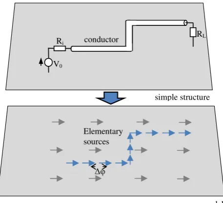
According to II transmission lines on planar structures, esp. PCBs, can also be approximated with elementary dipoles. With knowledge of the current paths, e.g. based on CAD-data, the approximating dipoles can be distributed along these paths
(Figure 2). Where Ri and RL are the terminating impedances
and V0 is the exciting input voltage. The number of dipoles is
chosen following (3). This approach, in comparison with the method of equally distributed dipoles, can considerable reduce the amount of necessary elementary sources, decrease computational cost and increase the model accuracy.
Dependencies between the neighboring elementary sources of each current path are used to correlate phases of the dipoles. For the spatial distribution ∆d the phase shift between two adjacent dipoles is set to
d ∆ = ∆ λ π
ϕ 2 (6)
as shown in Figure 2. With adherence to (6) phase jumps between two sources different from ∆φ are prevented and the model becomes more physically.
Figure 2. Drawing of the test board (above), model of the board (below) with equally distributed sources (grey) and sources only along the current path
(blue)
To compute the dipole moments M the magnetic near-field has to be measured in a plane above the planar structure. Afterwards the system of equations
I 1H
0 −
Α
= (7)
where Α contains the wave vector k0 and the fixed
geometric parameters for each dipole and H the complex magnetic field at K near-field points is solved.
For integrating the correlation between sources into model creation the inverse problem can be treated with the expandable minimization function F following (7).
(
H x y z H x y z)
Mine M z y x e M z y x F T N N N T M m j m N N N m j m M m m m m → − =
∑
∑
= − − = ) , , ( ),..., , , ( ) , , ( ,..., ) , , ( 0 1 1 1 0 1 1 1 1 1 ϕ ϕ α α (8)With αm are the fixed geometric parameters at observation point xn, yn, zn, the amplitude and Mm is and the phase e-j
φm
of
Ri conductor
RL simple structure ∆φ Elementary sources V0 model Ground Plane
V0(t) Ri Cable
ECU ECU
E(t),H(t)
Ze
Fig. 1. Simple configuration to investigate.
As main sources for emission of PCBs are the conducting traces, the distribution of the approximating sources can be bounded to the routing geometry. Furthermore techniques for correlating the properties of the approximating sources to compute a more physically model can be integrated in the model creation process. This can reduce the number of free source parameters and computation time. Furthermore the possibility of error correction is given and accuracy of the results increases.
In this paper a method for source identification of trans-mission lines, in form of cables bundles and conducting paths on PCBs, with considering correlations between the sources is presented. Investigations are done in a frequency range up to 500 MHz. The generated model enables different types of postprocessing e.g. far field estimations.
2 Source identification of cable bundles
As shown in Rinas et al., 2010 the current distribution of a radiating single cable (Fig. 1) can be estimated by measuring the magnetic field in at least two field points along the cable.
When calculation is based on two measurement sets
Iz=
1
2Z(Ve+ZIe)e
jβ(l−z)+ 1
2Z(Ve−ZIe)e
−jβ(l−z) (1)
with Ve Ie =
a1b1
a2b2 −1
·
I1(z1)
I2(z2)
(2) leads to currentIzat positionz. WhereVeandIeare voltage
and current at the end of transmission line, Z is the wave impedance, β the propagation constant,l the length of the line, a andb include the propagation functions andI1 and
I2are the current values corresponding to the magnetic field data.
The current distribution can also be estimated directly by increasing the amount of measured field points along the ca-ble depending on the frequency with respect to
N=l/1d (3)
1d > 1
10λ (4)
II.
SOURCE IDENTIFICATION OF CABLE BUNDLES
As shown in [2] the current distribution of a radiating single
cable (Figure 1) can be estimated by measuring the magnetic
field in at least two field points along the cable.
Figure 1. Simple configuration to investigate
When calculation is based on two measurement sets
) ( ) ( ( ) 2 1 ) ( 2
1 j l z
e e z l j e e
z V ZI e
Z e
ZI V Z
I = + β − + − −β −
(1)
with
⋅ = − ) ( ) ( 2 2 1 1 1 2 2 1 1 z I z I b a b a I V e e (2)leads to current
I
zat position
z
. Where
V
eand
I
eare voltage
and current at the end of transmission line,
Z
is the wave
impedance, β the propagation constant,
l
the length of the line,
a
and
b
include the propagation functions and
I
1and
I
2are the
current values corresponding to the magnetic field data.
The current distribution can also be estimated directly by
increasing the amount of measured field points along the cable
depending on the frequency with respect to
d l
N = ∆ (3)
λ
10 1 >
∆d (4)
where
N
is the amount of measurement points and
∆
d
the
spatial discretization width between the neighboring points. For
achieving
I
zthe discrete current values are approximated to a
sinusoidal function with nonlinear regression algorithms.
In order to create an equivalent emission model elementary
electric dipoles are placed in a line along the cable path in a
height
h
over ground adopted from the cable, following (4). The
dipole moments
M
1…M
Kare calculated with
2 1
+
+ ∆
= k k
k
I I d
M (5)
where
I
kis the discretized current
I
z.
III.
SOURCE IDENTIFICATION OF CONDUCTING TRACES ON
PLANAR STRUCTURESAccording to II transmission lines on planar structures, esp.
PCBs, can also be approximated with elementary dipoles. With
knowledge of the current paths, e.g. based on CAD-data, the
approximating dipoles can be distributed along these paths
(Figure 2). Where
R
iand
R
Lare the terminating impedances
and
V
0is the exciting input voltage. The number of dipoles is
chosen following
(3). This approach, in comparison with themethod of equally distributed dipoles, can considerable reduce
the amount of necessary elementary sources, decrease
computational cost and increase the model accuracy.
Dependencies between the neighboring elementary sources
of each current path are used to correlate phases of the dipoles.
For the spatial distribution
∆
d
the phase shift between two
adjacent dipoles is set to
d ∆ = ∆ λ π
ϕ 2 (6)
as shown in Figure 2. With adherence to (6) phase jumps
between two sources different from
∆φ are prevented and the
model becomes more physically.
Figure 2. Drawing of the test board (above), model of the board (below) with equally distributed sources (grey) and sources only along the current path
(blue)
To compute the dipole moments
M
the magnetic near-field
has to be measured in a plane above the planar structure.
Afterwards the system of equations
I 1H
0
−
Α
= (7)
where
Α contains the wave vector
k
0and the fixed
geometric parameters for each dipole and
H
the complex
magnetic field at
K
near-field points is solved.
For integrating the correlation between sources into model
creation the inverse problem can be treated with the
expandable minimization function
F
following (7).
(
H x y z H x y z)
Mine M z y x e M z y x F T N N N T M m j m N N N m j m M m m m m → − =
∑
∑
= − − = ) , , ( ),..., , , ( ) , , ( ,..., ) , , ( 0 1 1 1 0 1 1 1 1 1 ϕ ϕ α α (8)With α
mare the fixed geometric parameters at observation
point
x
n, y
n, z
n, the amplitude and
M
mis and the phase
e
-jφmof
Ri conductor
RL simple structure ∆φ Elementary sources V0 model
Ground Plane
V
0(t)
R
iCable
ECU
ECU
E(t),H(t)
Z
eFig. 2. Drawin g of the test board (above), model of the board
(below) with equally distributed sources (grey) and sources only along the current path (blue).
whereN is the amount of measurement points and1d the spatial discretization width between the neighboring points. For achievingIzthe discrete current values are approximated
to a sinusoidal function with nonlinear regression algorithms. In order to create an equivalent emission model elemen-tary electric dipoles are placed in a line along the cable path in a heighthover ground adopted from the cable, following 3. The dipole momentsM1...MKare calculated with Mk=1d
Ik+Ik+1
2 (5)
whereIk is the discretized currentIz.
3 Source identification of conducting traces on planar structures
According to Table 2 transmission lines on planar struc-tures, esp. PCBs, can also be approximated with elementary dipoles. With knowledge of the current paths, e.g. based on CAD-data, the approximating dipoles can be distributed along these paths (Fig. 2). WhereRi andRLare the
D. Rinas and S. Frei: Two methods for transmission line simulation model creation 119
each dipole. H0(xn, yn, zn) stands for the measured reference
field at observation points. Optimization methods are used for solving the minimization problem.
IV. RESULTS A. Cable Bundles
This chapter presents the results for model creation process of a single radiating cable and a small bundle. Some results are presently derived from an electromagnetic full field solver [10].
The input signal V0 (Figure 1, Figure 3) is a pulsed signal
with an amplitude V0 = 5 V, a fundamental frequency of
f0 = 4 MHz, a pulse/pause ratio th/tl = 1, and a rising and falling edge of tr,f = 2.5 ns. Source impedance Ri is 50-Ohm.
1) Single Conductor – Measurement Based Results
The cable (Figure 3) consists of a single conductor placed in the height h = 50 mm over a ground plane. It has a length of
l = 490 mm and a thickness of d = 1 mm. It is terminated with a
Ze = 50 Ω impedance. The magnetic field is measured at two
positions y1 = 120 mm and y2 = 360 mm along the cable at a
height hS = 20 mm over ground.
Figure 3. Single conductor under test
With the identified sources the magnetic field is calculated at a position p1 = (3, 3, 3)T [m]. Exemplary the fields of the
fundamental wave and the 2th, 7th, 15th and 20thharmonics of the pulsed input signal are presented in TABLE 1. As a comparison a full field simulation of the cable under test given by a MoM solver [10] is shown. The results agree with a maximum error of 3 dB.
TABLE I. MAGNETIC FIELD OF MEASUREMENT BASED MODEL AT P1 IN COMPARSION WITH FULL FIELD SIMULATION
Frequency
Magnitude [dBµA/m]
Sim. Model
4 MHz 29.4963 26.3542
20 MHz 32.4243 32.9482
60 MHz 36.7945 37.3562
124 MHz 43.1243 45.2324 164 MHz 47.7698 50.1270
2) Single Conductor – Simulation Based Results
The following investigations are presently based on computer simulations.
The cable (Figure 3) consists of a single conductor placed in the height h = 10 mm over the ground plane. It has a length of l = 600 mm and a thickness of d = 0.3 mm. It is terminated with a serial circuit of resistor Re = 50 Ωand inductance Le =
1 µH. The model parameters are taken from the cable under test. The source internal resistance is set to Ri = 50 Ω. The
magnetic field is measured at two positions y1 = 200 mm and
y2 = 400 mm along the cable at a height hS = 20 mm over
ground.
Figure 4 shows the magnetic field at point p1 ina frequency
range of 1 MHz to 500 MHz. The results in comparison with the full field simulation agree with maximum error of about 3 dB.
1 10 100 500
-50 -40 -30 -20 -10 0 10
Frequency [MHz]
M
a
g
n
it
u
d
e
[
d
B
u
A
/m
]
full field simulation equivalent dipole model
Figure 4. Magnetic field at p1 in comparison with full field simulation
3) Multiconductor – Simulation Based Results
The following investigations are presently based on computer simulations.
The multiconductor (Figure 5) consists of three single conductors placed in the height of h = 10 mm over ground plane. The length of each conductor is l = 600 mm; the thickness is d = 0.3 mm and they are arranged in a distance of
D = 5 mm. The internal source resistances are set to Ri = 50 Ω.
The terminations are Ze1= 50 Ω || jω·0.1nF, Ze2= 50Ω,
Ze3= 50 Ω + jω·1µH. The excitation is impressed in the center
conductor.
Figure 5. Multiconductor under test D
l V0
Ri
Ze1
h
Ze2
Ze3
l
V0
Ri Ze
h
magnetic field probe
hs
ground
ground Fig. 3. Single conductor under test.
Dependencies between the neighboring elementary sources of each current path are used to correlate phases of the dipoles. For the spatial distribution1d the phase shift between two adjacent dipoles is set to
1ϕ=2π
λ 1d (6)
as shown in Fig. 2. With adherence to Eq. (6) phase jumps between two sources different from 1φ are prevented and the model becomes more physically.
To compute the dipole momentsMthe magnetic near-field has to be measured in a plane above the planar structure. Af-terwards the system of equations
I0=A−1H (7)
where A contains the wave vectork0and the fixed geometric parameters for each dipole andHthe complex magnetic field atKnear-field points is solved.
For integrating the correlation between sources into model creation the inverse problem can be treated with the expand-able minimization functionF following 4.
F=
M
X
m=1
αm(x1,y1,z1)Mme−j ϕm,...,
M
X
m=1
αm(xN,yN,zN)Mme−j ϕm
!T
−(H0(x1,y1,z1),...,H0(xN,yN,zN))T →Min (8)
Withαm are the fixed geometric parameters at observation
point xn,yn,zn, the amplitude and Mm is and the phase e−j φmof each dipole.H0(xn,yn,zn)stands for the measured
reference field at observation points. Optimization methods are used for solving the minimization problem.
each dipole.
H
0(x
n, y
n, z
n)
stands for the measured reference
field at observation points. Optimization methods are used for
solving the minimization problem.
IV.
R
ESULTSA.
Cable Bundles
This chapter presents the results for model creation process
of a single radiating cable and a small bundle. Some results are
presently derived from an electromagnetic full field solver [10].
The input signal
V
0(Figure 1, Figure 3) is a pulsed signal
with an amplitude
V
0= 5 V
, a fundamental frequency of
f
0= 4 MHz
, a pulse/pause ratio t
h/t
l= 1, and a rising and falling
edge of t
r,f= 2.5 ns. Source impedance
R
iis 50-Ohm.
1)
Single Conductor – Measurement Based Results
The cable (Figure 3) consists of a single conductor placed
in the height
h = 50 mm
over a ground plane. It has a length of
l = 490 mm
and a thickness of
d = 1 mm
. It is terminated with a
Z
e= 50
Ω impedance. The magnetic field is measured at two
positions
y
1= 120 mm
and
y
2= 360 mm
along the cable at a
height
h
S= 20 mm
over ground.
Figure 3. Single conductor under test
With the identified sources the magnetic field is calculated
at a position
p
1= (3, 3, 3)
T
[m]
. Exemplary the fields of the
fundamental wave and the
2
th,
7
th,
15
thand
20
thharmonics of
the pulsed input signal are presented in TABLE 1. As a
comparison a full field simulation of the cable under test given
by a MoM solver [10] is shown. The results agree with a
maximum error of
3 dB
.
TABLE I. MAGNETIC FIELD OF MEASUREMENT BASED MODEL AT P1 IN COMPARSION WITH FULL FIELD SIMULATION
Frequency
Magnitude [dBµA/m]
Sim. Model
4 MHz 29.4963 26.3542
20 MHz 32.4243 32.9482
60 MHz 36.7945 37.3562
124 MHz 43.1243 45.2324
164 MHz 47.7698 50.1270
2)
Single Conductor – Simulation Based Results
The following investigations are presently based on
computer simulations.
The cable (Figure 3) consists of a single conductor placed
in the height
h = 10 mm
over the ground plane. It has a length
of
l = 600 mm
and a thickness of
d = 0.3 mm
. It is terminated
with a serial circuit of resistor
R
e= 50
Ω
and inductance
L
e=
1
µ
H
. The model parameters are taken from the cable under
test. The source internal resistance is set to
R
i= 50
Ω. The
magnetic field is measured at two positions
y
1= 200 mm
and
y
2= 400 mm
along the cable at a height
h
S= 20 mm
over
ground.
Figure 4 shows the magnetic field at point
p
1in
a frequency
range of
1 MHz
to
500 MHz
. The results in comparison with
the full field simulation agree with maximum error of about
3
dB
.
1 10 100 500
-50 -40 -30 -20 -10 0 10
Frequency [MHz]
M
a
g
n
it
u
d
e
[
d
B
u
A
/m
]
full field simulation equivalent dipole model
Figure 4. Magnetic field at p1 in comparison with full field simulation
3)
Multiconductor – Simulation Based Results
The following investigations are presently based on
computer simulations.
The multiconductor (Figure 5) consists of three single
conductors placed in the height of
h = 10 mm
over ground
plane. The length of each conductor is
l = 600 mm
; the
thickness is
d = 0.3 mm
and they are arranged in a distance of
D = 5 mm
. The internal source resistances are set to
R
i= 50
Ω.
The terminations are
Z
e1= 50
Ω
|| j
ω
·0.1nF
,
Z
e2= 50
Ω
,
Z
e3= 50
Ω
+ j
ω
·1
µ
H
. The excitation is impressed in the center
conductor.
Figure 5. Multiconductor under test D
l V0
Ri
Ze1
h
Ze2
Ze3
l
V0
Ri Z
e
h
magnetic field probe
hs
ground
ground
Fig. 4. Magnetic field atp1in comparison with full field simulation.
Table 1. Magnetic Field of Measurement based Model atp1 in comparsion with full field simulation.
Frequency Magnitude [dBµ A/m]
Sim. Model
4 MHz 29.4963 26.3542
20 MHz 32.4243 32.9482
60 MHz 36.7945 37.3562
124 MHz 43.1243 45.2324
164 MHz 47.7698 50.1270
4 Results
4.1 Cable bundles
This chapter presents the results for model creation process of a single radiating cable and a small bundle. Some re-sults are presently derived from an electromagnetic full field solver (EMCoS Consulting and Software, www.emcos.com). The input signal V0 (Figs. 1 and 3) is a pulsed signal with an amplitudeV0 = 5 V, a fundamental frequency of
f0 = 4 MHz, a pulse/pause ratio th/tl = 1, and a rising
and falling edge oftr,f = 2.5 ns. Source impedanceRi is
50 Ohm.
4.1.1 Single conductor – measurement based results
The cable (Fig. 3) consists of a single conductor placed in the height h = 50 mm over a ground plane. It has a length of l = 490 mm and a thickness of d = 1 mm. It is terminated with aZe = 50impedance. The magnetic field is measured at
two positionsy1= 120 mm andy2= 360 mm along the cable at a heighthS= 20 mm over ground.
With the identified sources the magnetic field is calculated at a positionp1= (3, 3, 3)T[m]. Exemplary the fields of the fundamental wave and the 2th, 7th, 15th and 20th harmon-ics of the pulsed input signal are presented in Table 1. As a comparison a full field simulation of the cable under test given by a MoM solver (EMCoS Consulting and Software, www.emcos.com) is shown. The results agree with a maxi-mum error of 3 dB.
120 D. Rinas and S. Frei: Two methods for transmission line simulation model creation
Table 2. Near-Fields of different Models in Comparison with full
field simulation.
In Figure 6 the magnetic field at point p1 in comparison with the full field simulation is shown. The magnetic field agrees with a maximum error of 3 dB at most frequencies.
1 10 100 500 -40 -30 -20 -10 0 10 Frequency [MHz] M a g n it u d e [ d B u A /m )
full field simulation equivalent dipole model
Figure 6. Magnetic field at p1 in comparison with full field simulation
B. Printed Circuit Boards – Simulation Based Results
A simple planar structure is analyzed. It consists of a 0.1 x 0.1 m plane and a conductor with total length of 0.16 m. The source voltage is 1 Volt; termination is a 50 Ohm resistance. The magnetic field is measured in a height of 0.01 m over ground at 256 near-field points. The source parameters are computed with amplitude-data only. Simulated Annealing is used as optimization method for model parameter calculation.
In TABLE II near-field calculations from different models are shown and compared with a full field simulation (MoM) of the planar structure at a frequency of 100 MHz. Figure 7 shows the magnetic field at point p1 = (3, 3, 3)
T
[m] in comparison
with the full field simulation in a frequency range of 1 MHz to 500 MHz.
As presented, the field approximation shows better accuracy if the distribution of sources is matched with the current distribution depending on the conductor path. The result plots show also a smaller deviation if the phase correlation between sources is integrated in the model computation.
TABLE II. NEAR-FIELDS OF DIFFERENT MODELS IN COMPARISON WITH FULL FIELD SIMULATION
Full field simulation
Equally distributed sources Sources along current path
No phase correlation of sources With phase correlation of sources
1 10 100 200 500 -160 -140 -120 -100 -80 -60 -40 Frequency [MHz] M a g n e ti c F ie ld [ d B V /m ]
Full field simulation
Equally distributed sources; without phase correlation Sources along current path; without phase correlation Sources along current path; with phase correlation
Figure 7. Magnetic field at p1 for different source distribution in comparison with full field simulation
V. CONCLUSION
In this paper methods for source identification of radiating transmission lines are presented. The focus is on cables bundles and conducting traces on planar structures. Model accuracy is can be increased by considering correlation between the neighboring approximating sources.
The approaches were tested by simulations and first measurements and were compared with numerical full field simulation data.
REFERENCES
[1] “CISPR 25 Ed.3: Vehicles, boats and internal combustion engines – Radio disturbance characteristics – Limits and methods of measurement for the protection of on-board receivers”.
[2] D. Rinas, S. Niedzwiedz, S. Frei, “Far Field Estimations and Simulation Model Creation from Cable Bundle Scans”, EMC Europe, Wroclaw, 2010
[3] Constantine A. Balanis, “Antenna Theory Analysis & Design”, Wiley, 1996.
[4] Yolanda Vives Gilabert, “Modélisation des emissions rayonées de composants électroniques”, Université de Rouen, 2007.
[5] D. Baudry, M. Kadi, Z. Riah, C. Arcambal, Y. Vives-Gilabert, A. Louis, B. Mazari, “Plane wave spectrum theory applied to near-field measurements for electromagnetic compatibility investigations”, IET Science, Measurement and Technology, 15. June 2008.
[6] Tommaso Isernia, Giovanni Leone, Rocco Pierri, “Radiation Pattern Evaluation from Near-Field Intensities on Planes”, IEEE Transaction on Antennas and Propagation, Vol. 44, No. 5, May 1996.
[7] Xin Tong, D.W.P. Thomas, A. Nothofer, P. Sewell, C. Christopoulos, “A Genetic Algorithm Based Method for Modeling Equivalent Emission Sources of Printed Circuits from Near-Field Measurements”, APEMC Beijing, 2010.
[8] T. Isernia, G. Leone, R. Pierri, “Radiation pattern evaluation from near-field intensities on planes,” IEEE Trans. Antennas Propogat., vol. 44, pp. 701–710, May 1996.
[9] R. Pierri, G. D’Elia, F. Soldovieri, “A two probes scanning phaseless near-field far-field transformation technique,” IEEE Trans. Antennas Propogat., vol. 47, pp. 792–802, May 1999.
[10] EMCoS Consulting and Software, www.emcos.com each dipole. H0(xn, yn, zn) stands for the measured reference
field at observation points. Optimization methods are used for solving the minimization problem.
IV. RESULTS A. Cable Bundles
This chapter presents the results for model creation process of a single radiating cable and a small bundle. Some results are presently derived from an electromagnetic full field solver [10].
The input signal V0 (Figure 1, Figure 3) is a pulsed signal
with an amplitude V0 = 5 V, a fundamental frequency of
f0 = 4 MHz, a pulse/pause ratio th/tl = 1, and a rising and falling edge of tr,f = 2.5 ns. Source impedance Ri is 50-Ohm.
1) Single Conductor – Measurement Based Results
The cable (Figure 3) consists of a single conductor placed in the height h = 50 mm over a ground plane. It has a length of
l = 490 mm and a thickness of d = 1 mm. It is terminated with a
Ze = 50 Ω impedance. The magnetic field is measured at two
positions y1 = 120 mm and y2 = 360 mm along the cable at a
height hS = 20 mm over ground.
Figure 3. Single conductor under test
With the identified sources the magnetic field is calculated at a position p1 = (3, 3, 3)
T
[m]. Exemplary the fields of the fundamental wave and the 2th, 7th, 15th and 20thharmonics of the pulsed input signal are presented in TABLE 1. As a comparison a full field simulation of the cable under test given by a MoM solver [10] is shown. The results agree with a maximum error of 3 dB.
TABLE I. MAGNETIC FIELD OF MEASUREMENT BASED MODEL AT P1 IN COMPARSION WITH FULL FIELD SIMULATION
Frequency
Magnitude [dBµA/m]
Sim. Model
4 MHz 29.4963 26.3542 20 MHz 32.4243 32.9482 60 MHz 36.7945 37.3562 124 MHz 43.1243 45.2324 164 MHz 47.7698 50.1270
2) Single Conductor – Simulation Based Results
The following investigations are presently based on computer simulations.
The cable (Figure 3) consists of a single conductor placed in the height h = 10 mm over the ground plane. It has a length of l = 600 mm and a thickness of d = 0.3 mm. It is terminated with a serial circuit of resistor Re = 50 Ωand inductance Le =
1 µH. The model parameters are taken from the cable under test. The source internal resistance is set to Ri = 50 Ω. The
magnetic field is measured at two positions y1 = 200 mm and
y2 = 400 mm along the cable at a height hS = 20 mm over
ground.
Figure 4 shows the magnetic field at point p1 ina frequency
range of 1 MHz to 500 MHz. The results in comparison with the full field simulation agree with maximum error of about 3 dB.
1 10 100 500
-50 -40 -30 -20 -10 0 10 Frequency [MHz] M a g n it u d e [ d B u A /m ]
full field simulation equivalent dipole model
Figure 4. Magnetic field at p1 in comparison with full field simulation
3) Multiconductor – Simulation Based Results
The following investigations are presently based on computer simulations.
The multiconductor (Figure 5) consists of three single conductors placed in the height of h = 10 mm over ground plane. The length of each conductor is l = 600 mm; the thickness is d = 0.3 mm and they are arranged in a distance of
D = 5 mm. The internal source resistances are set to Ri = 50 Ω.
The terminations are Ze1= 50 Ω || jω·0.1nF, Ze2= 50Ω,
Ze3= 50 Ω + jω·1µH. The excitation is impressed in the center
conductor.
Figure 5. Multiconductor under test D l V0 Ri Ze1 h Ze2 Ze3 l V0
Ri Ze
h
magnetic field probe
hs
ground
ground
Fig. 5. Multiconductor under test.
4.1.2 Single conductor – simulation based results The following investigations are presently based on com-puter simulations.
The cable (Fig. 3) consists of a single conductor placed in the height h = 10 mm over the ground plane. It has a length of l = 600 mm and a thickness of d = 0.3 mm. It is terminated with a serial circuit of resistorRe= 50and inductanceLe=
1 µH. The model parameters are taken from the cable under test. The source internal resistance is set toRi = 50. The
magnetic field is measured at two positionsy1= 200 mm and
y2= 400 mm along the cable at a heighthS = 20 mm over
ground.
Figure 4 shows the magnetic field at point p1 in a fre-quency range of 1 MHz to 500 MHz. The results in com-parison with the full field simulation agree with maximum error of about 3 dB.
4.1.3 Multiconductor – simulation based results The following investigations are presently based on com-puter simulations.
The multiconductor (Fig. 5) consists of three single con-ductors placed in the height of h = 10 mm over ground
In Figure 6 the magnetic field at point p1 in comparison with the full field simulation is shown. The magnetic field agrees with a maximum error of 3 dB at most frequencies.
1 10 100 500
-40 -30 -20 -10 0 10 Frequency [MHz] M a g n it u d e [ d B u A /m )
full field simulation equivalent dipole model
Figure 6. Magnetic field at p1 in comparison with full field simulation
B. Printed Circuit Boards – Simulation Based Results
A simple planar structure is analyzed. It consists of a 0.1 x 0.1 m plane and a conductor with total length of 0.16 m. The source voltage is 1 Volt; termination is a 50 Ohm resistance. The magnetic field is measured in a height of 0.01 m over ground at 256 near-field points. The source parameters are computed with amplitude-data only. Simulated Annealing is used as optimization method for model parameter calculation.
In TABLE II near-field calculations from different models are shown and compared with a full field simulation (MoM) of the planar structure at a frequency of 100 MHz. Figure 7 shows the magnetic field at point p1 = (3, 3, 3)
T
[m] in comparison with the full field simulation in a frequency range of 1 MHz to 500 MHz.
As presented, the field approximation shows better accuracy if the distribution of sources is matched with the current distribution depending on the conductor path. The result plots show also a smaller deviation if the phase correlation between sources is integrated in the model computation.
TABLE II. NEAR-FIELDS OF DIFFERENT MODELS IN COMPARISON WITH FULL FIELD SIMULATION
Full field simulation
Equally distributed sources Sources along current path
No phase correlation of sources With phase correlation of sources
1 10 100 200 500
-160 -140 -120 -100 -80 -60 -40 Frequency [MHz] M a g n e ti c F ie ld [ d B V /m ]
Full field simulation
Equally distributed sources; without phase correlation Sources along current path; without phase correlation Sources along current path; with phase correlation
Figure 7. Magnetic field at p1 for different source distribution in comparison
with full field simulation
V. CONCLUSION
In this paper methods for source identification of radiating transmission lines are presented. The focus is on cables bundles and conducting traces on planar structures. Model accuracy is can be increased by considering correlation between the neighboring approximating sources.
The approaches were tested by simulations and first measurements and were compared with numerical full field simulation data.
REFERENCES
[1] “CISPR 25 Ed.3: Vehicles, boats and internal combustion engines – Radio disturbance characteristics – Limits and methods of measurement for the protection of on-board receivers”.
[2] D. Rinas, S. Niedzwiedz, S. Frei, “Far Field Estimations and Simulation Model Creation from Cable Bundle Scans”, EMC Europe, Wroclaw, 2010
[3] Constantine A. Balanis, “Antenna Theory Analysis & Design”, Wiley, 1996.
[4] Yolanda Vives Gilabert, “Modélisation des emissions rayonées de composants électroniques”, Université de Rouen, 2007.
[5] D. Baudry, M. Kadi, Z. Riah, C. Arcambal, Y. Vives-Gilabert, A. Louis, B. Mazari, “Plane wave spectrum theory applied to near-field measurements for electromagnetic compatibility investigations”, IET Science, Measurement and Technology, 15. June 2008.
[6] Tommaso Isernia, Giovanni Leone, Rocco Pierri, “Radiation Pattern Evaluation from Near-Field Intensities on Planes”, IEEE Transaction on Antennas and Propagation, Vol. 44, No. 5, May 1996.
[7] Xin Tong, D.W.P. Thomas, A. Nothofer, P. Sewell, C. Christopoulos, “A Genetic Algorithm Based Method for Modeling Equivalent Emission Sources of Printed Circuits from Near-Field Measurements”, APEMC Beijing, 2010.
[8] T. Isernia, G. Leone, R. Pierri, “Radiation pattern evaluation from near-field intensities on planes,” IEEE Trans. Antennas Propogat., vol. 44, pp. 701–710, May 1996.
[9] R. Pierri, G. D’Elia, F. Soldovieri, “A two probes scanning phaseless near-field far-field transformation technique,” IEEE Trans. Antennas Propogat., vol. 47, pp. 792–802, May 1999.
[10] EMCoS Consulting and Software, www.emcos.com
Fig. 6. Magnetic field atp1in comparison with full field simulation.
In Figure 6 the magnetic field at point p1 in comparison with the full field simulation is shown. The magnetic field agrees with a maximum error of 3 dB at most frequencies.
1 10 100 500
-40 -30 -20 -10 0 10 Frequency [MHz] M a g n it u d e [ d B u A /m )
full field simulation equivalent dipole model
Figure 6. Magnetic field at p1 in comparison with full field simulation
B. Printed Circuit Boards – Simulation Based Results
A simple planar structure is analyzed. It consists of a 0.1 x 0.1 m plane and a conductor with total length of 0.16 m. The source voltage is 1 Volt; termination is a 50 Ohm resistance. The magnetic field is measured in a height of 0.01 m over ground at 256 near-field points. The source parameters are computed with amplitude-data only. Simulated Annealing is used as optimization method for model parameter calculation.
In TABLE II near-field calculations from different models are shown and compared with a full field simulation (MoM) of the planar structure at a frequency of 100 MHz. Figure 7 shows the magnetic field at point p1 = (3, 3, 3)
T
[m] in comparison with the full field simulation in a frequency range of 1 MHz to 500 MHz.
As presented, the field approximation shows better accuracy if the distribution of sources is matched with the current distribution depending on the conductor path. The result plots show also a smaller deviation if the phase correlation between sources is integrated in the model computation.
TABLE II. NEAR-FIELDS OF DIFFERENT MODELS IN COMPARISON WITH FULL FIELD SIMULATION
Full field simulation
Equally distributed sources Sources along current path
No phase correlation of sources
With phase correlation
1 10 100 200 500
-160 -140 -120 -100 -80 -60 -40 Frequency [MHz] M a g n e ti c F ie ld [ d B V /m ]
Full field simulation
Equally distributed sources; without phase correlation Sources along current path; without phase correlation Sources along current path; with phase correlation
Figure 7. Magnetic field at p1 for different source distribution in comparison
with full field simulation
V. CONCLUSION
In this paper methods for source identification of radiating transmission lines are presented. The focus is on cables bundles and conducting traces on planar structures. Model accuracy is can be increased by considering correlation between the neighboring approximating sources.
The approaches were tested by simulations and first measurements and were compared with numerical full field simulation data.
REFERENCES
[1] “CISPR 25 Ed.3: Vehicles, boats and internal combustion engines – Radio disturbance characteristics – Limits and methods of measurement for the protection of on-board receivers”.
[2] D. Rinas, S. Niedzwiedz, S. Frei, “Far Field Estimations and Simulation Model Creation from Cable Bundle Scans”, EMC Europe, Wroclaw, 2010
[3] Constantine A. Balanis, “Antenna Theory Analysis & Design”, Wiley, 1996.
[4] Yolanda Vives Gilabert, “Modélisation des emissions rayonées de composants électroniques”, Université de Rouen, 2007.
[5] D. Baudry, M. Kadi, Z. Riah, C. Arcambal, Y. Vives-Gilabert, A. Louis, B. Mazari, “Plane wave spectrum theory applied to near-field measurements for electromagnetic compatibility investigations”, IET Science, Measurement and Technology, 15. June 2008.
[6] Tommaso Isernia, Giovanni Leone, Rocco Pierri, “Radiation Pattern Evaluation from Near-Field Intensities on Planes”, IEEE Transaction on Antennas and Propagation, Vol. 44, No. 5, May 1996.
[7] Xin Tong, D.W.P. Thomas, A. Nothofer, P. Sewell, C. Christopoulos, “A Genetic Algorithm Based Method for Modeling Equivalent Emission Sources of Printed Circuits from Near-Field Measurements”, APEMC Beijing, 2010.
[8] T. Isernia, G. Leone, R. Pierri, “Radiation pattern evaluation from near-field intensities on planes,” IEEE Trans. Antennas Propogat., vol. 44, pp. 701–710, May 1996.
[9] R. Pierri, G. D’Elia, F. Soldovieri, “A two probes scanning phaseless near-field far-field transformation technique,” IEEE Trans. Antennas Propogat., vol. 47, pp. 792–802, May 1999.
Fig. 7. Magnetic field atp1for different source distribution in
com-parison with full field simulation.
plane. The length of each conductor is l = 600 mm; the thickness is d = 0.3 mm and they are arranged in a dis-tance of D = 5 mm. The internal source resisdis-tances are set toRi=50. The terminations areZe1=50||j ω·0.1 nF,
Ze2=50, Ze3=50+j ω·1 µH. The excitation is im-pressed in the center conductor.
In Fig. 6 the magnetic field at pointp1in comparison with the full field simulation is shown. The magnetic field agrees with a maximum error of 3 dB at most frequencies.
4.2 Printed circuit boards – simulation based results
A simple planar structure is analyzed. It consists of a 0.1×0.1 m plane and a conductor with total length of 0.16 m. The source voltage is 1 Volt; termination is a 50 Ohm resis-tance. The magnetic field is measured in a height of 0.01 m over ground at 256 near-field points. The source parameters are computed with amplitude-data only. Simulated Anneal-ing is used as optimization method for model parameter cal-culation.
In Table 2 near-field calculations from different models are shown and compared with a full field simulation (MoM) of
D. Rinas and S. Frei: Two methods for transmission line simulation model creation 121 the planar structure at a frequency of 100 MHz. Figure 7
shows the magnetic field at pointp1 = (3,3,3)T[m]in com-parison with the full field simulation in a frequency range of 1 MHz to 500 MHz.
As presented, the field approximation shows better accu-racy if the distribution of sources is matched with the cur-rent distribution depending on the conductor path. The result plots show also a smaller deviation if the phase correlation between sources is integrated in the model computation.
5 Conclusions
In this paper methods for source identification of radiating transmission lines are presented. The focus is on cables bun-dles and conducting traces on planar structures. Model accu-racy is can be increased by considering correlation between the neighboring approximating sources.
The approaches were tested by simulations and first mea-surements and were compared with numerical full field sim-ulation data.
References
CISPR 25 Ed.3: Vehicles, boats and internal combustion engines – Radio disturbance characteristics – Limits and methods of mea-surement for the protection of on-board receivers, 2008. Rinas, D., Niedzwiedz, S., and Frei, S.: Far Field Estimations and
Simulation Model Creation from Cable Bundle Scans, EMC Eu-rope, Wroclaw, 203–208, 2010.
Balanis, C. A.: Antenna Theory Analysis & Design, Wiley, 1996. Vives-Gilabert, Y.: Mod´elisation des emissions rayon´ees de
com-posants ´electroniques, Universit´e de Rouen, 2007.
Baudry, D., Kadi, M., Riah, Z., Arcambal, C., Vives-Gilabert, Y., Louis, A., and Mazari, B.: Plane wave spectrum theory applied to near-field measurements for electromagnetic compatibility inves-tigations”, IET Science, Measurement and Technology, 15 June 2008.
Isernia, T., Giovanni Leone, G. and Pierri, R.: Radiation Pattern Evaluation from Near-Field Intensities on Planes, IEEE Transac-tion on Antennas and PropagaTransac-tion, 44(5), 701–710, 1996. Tong, X., Thomas, D. W. P., Nothofer, A., Sewell, P., and
Christopoulos, C.: A Genetic Algorithm Based Method for Modeling Equivalent Emission Sources of Printed Circuits from Near-Field Measurements, APEMC Beijing, 2010.
Isernia, T., Leone, G., and Pierri, R.: Radiation pattern evaluation from near-field intensities on planes, IEEE Trans. Antennas Pro-pogat., 44, 701–710, 1996.
Pierri, R., D’Elia, G., and Soldovieri, F.: A two probes scanning phaseless near-field far-field transformation technique, IEEE Trans. Antennas Propogat., 47, 792–802, 1999.
EMCoS Consulting and Software, www.emcos.com, January 2011.