Journal of Computing and Security
http://www.jcomsec.org
A High Speed Residue-to-Binary Converter for Balanced 4-Moduli
Set
MohammadReza Taheri
a, Nasim Shafiee
a, Mohammad Esmaeildoust
b,
Zhale Amirjamshidi
c, Reza Sabbaghi-nadooshan
c, Keivan Navi
a,∗
aFaculty of Computer Science and Engineering, Shahid Beheshti University, GC, Tehran, Iran.
bFaculty of Marine Engineering, Khorramshahr University of Marine Science and Technology, Khuzestan, Iran. cElectronic Engineering Department, Islamic Azad University, Central Tehran Branch, Tehran, Iran.
A R T I C L E I N F O.
Article history: Received:6 January 2014
Revised:7 November 2015
Accepted:7 December 2015
Published Online:7 February 2016
Keywords:
Mixed Radix Conversion, Residue Arithmetic, Residue Number System, Residue-to-Binary Converter
A B S T R A C T
The moduli set
2n−1−1,2n+1−1,2n,2n−1 has been recently proposed in literature for class of 4n-bit dynamic range in residue number system. Due to only utilizing modulus in the form of 2k−1 besides modulo 2n, this moduli set enjoys the efficient Arithmetic Unit (AU) in its architecture. Not only does the efficiency of a RNS system depend on the residue arithmetic unit but it also is limited to the residue to binary converter. In this paper, a new two level residue-to-binary converter architecture based on Mixed Radix Conversion (MRC) is presented for the aforementioned moduli set. The proposed converter includes two levels of design based on MRC properties. Firstly, the 3-moduli subset 2n−1−1,2n+1−1,2n−1 is properly organized and as it does not calculate several values, it results in some cost modifications. Eventually, a two-moduli set 2n−1−1 2n+1−1(2n−1),2n is formed to compute the binary of RNS counterpart. The proposed architecture is shown to be more efficient both in terms of hardware cost and conversion delay in comparison with the related state-of-the-art works.
c
2015 JComSec. All rights reserved.
1
Introduction
The carry-free nature of the residue number system (RNS) makes it suitable to be used in the arithmetic level in VLSI design to achieve parallelism [1], [2]. In RNS, a weighted number is decomposed into a set of residues. Since arithmetic operations on residues can be performed without carry propagation between them, RNS results in high-speed addition, subtraction
∗ Corresponding author.
Email addresses:moh [email protected](MR. Taheri), [email protected](N. Shafiee),m [email protected] (M. Esmaeildoust),[email protected](Z. Amirjamshidi), r [email protected](R. Sabbaghi-nadooshan), [email protected](K. Navi)
ISSN: 2322-4460 c2015 JComSec. All rights reserved.
and multiplication [3], [4], which is appropriate for dig-ital signal processing (DSP) [5], [6], image processing [7], cryptography [8], [9] and communication systems [10]. However, arithmetic operations like division, sign detection and comparison are difficult in RNS.
Table 1. Comparison of arithmetic operation for different moduli sets for high dynamic range applications
Moduli set Design Critical modulus Delay
{2n−1,2n,2n+ 1,2n+1−1} [13,14] 2n+ 1 2log2n+ 6
{2n−1,2n,2n+ 1,2n+1+ 1} [13,15] 2n+1+ 1 2log
2(n+ 1) + 6
{2n−3,2n−1,2n+ 1,2n+ 3} [16] 2n+ 3 2log2(n−1) + 7
{2n,2n+1−1,2n−1,2n−1−1} [17] 2n+1−1 2log
2(n+ 1) + 3
and reverse conversion. A reverse converter has more complex architecture and its complexity will grow depending on the number of modules. Therefore, an effective design of reverse converter is needed in order to get the benefit of the RNS [12].
Many works have been reported on balanced 4-moduli sets such as {2n −1,2n,2n + 1,2n+1−1}
[13,14,16],{2n−1,2n,2n+1,2n+1−1}[13,15],{2n−
3,2n−1,2n+ 1,2n+ 3}[16] and{2n,2n+1−1,2n−
1,2n−1−1}[17]. Efficiency of arithmetic operations
is restricted to critical modulus. The critical moduli in [13–17] are shown in Table 1. The unit gate de-lays of the parallel prefix adders 2k−1, 2k+ 1 and 2k+ 3 are 2log
2n+ 3,2log2n+ 6 and 2log2(n−1) + 7,
respectively [18–20]. Therefore, as it is shown in Ta-ble 1, moduli set {2n,2n+1 −1,2n −1,2n−1 −1}
[17] provides more effecient arithmetic unit. However, more efficient reverse converter for the moduli set
{2n,2n+1−1,2n−1,2n−1−1} with less hardware
requirements and delay, compared to [17] and other moduli sets in literature, is needed. Therefore, in this paper, a new design of the reverse converter for the 4-moduli set is presented. The proposed converter has achieved less delay and more desirable hardware re-quirements compared to the state-of-the-art convert-ers.
This paper consists of a background about RNS in Section 2, design of the proposed RNS to binary converter in Section3, evaluation of hardware require-ments and critical path delay of the proposed reverse converter in Section4, comparison of the performance of the proposed RNS to binary converter with other moduli sets in Section5and finally the conclusions of the paper in Section6.
2
Background
A residue number system is defined in terms of rel-atively prime moduli set {P1, P2, . . . , Pn} that is
gcd(Pi, Pj) = 1 for i 6= j. An integer numberX in the range of [0, M −1] can be represented as X = (x1, x2, . . . , xn) wherexi=XmodPi , 0 ≤xi ≤Pi, andM =P1×P2. . .×Pn is the dynamic range of the RNS system [21].
Reverse conversion algorithms are principally based on the Chinese remainder theorem (CRT), Mixed-radix conversion (MRC) and new Chinese remainder theorems (New CRTs) [11]. Through the MRC, the numberX can be calculated using
X =vn n−1
Y
i=1
Pi+· · ·+v3P2P1+v2P1+v1 (1)
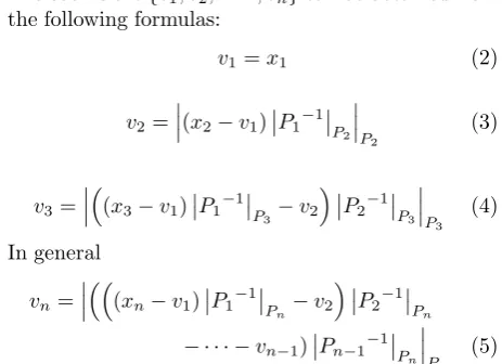
The coefficient{v1, v2, . . . , vn}can be obtained from the following formulas:
v1=x1 (2)
v2=
(x2−v1) P1−1
P
2 P
2
(3)
v3=
(x3−v1) P1−1
P
3−v2
P2−1 P
3 P
3 (4) In general
vn=
(xn−v1) P1−1
P
n−v2
P2−1
P
n
− · · · −vn−1) Pn−1−1
P
n
P
n
(5) WherePi−1
P
j is the multiplicative inverse ofPi
mod-uloPj [11].
Three types of adders are used to realize the hard-ware architecture of the reverse converter, Carry Save Adder (CSA) for operations in modulo 2n, CSA with End Around Carry (EAC) for operations in modulo 2k−1, Carry Propagate Adder (CPA) and Modular Adder (MA). For MA in modulo 2k−1, CPA with end around carry (EAC) is used, which has the similar area and double delay in comparison with a regular CPA [22]. These are explained more in Section4.
3
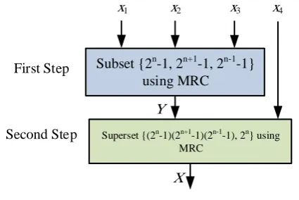
Proposed RNS to Binary Converter
The two-level architecture, realized by the MRC method, can lead to an efficient implementa-tion of RNS to binary converter of moduli set Ψ = 2n−1−1,2n+1−1,2n−1,2n . In the first step, number Y is calculated from the residues in the subset Γ =
Subset {2n-1, 2n+1-1, 2n-1-1} using MRC
x
1x
2Superset {(2n-1)(2n+1-1)(2n-1-1), 2n} using MRC
X
3x
Y
x
4 First Step Second StepFigure 1. Proposed Schema for residue-to-binary conversion
using MRC in a parallel manner. In the second step, the MRC method is applied to the superset
Λ =
2n−1−1
2n+1−1
(2n−1),2n and the final result is realized. The proposed reverse converter scheme is composed of two parts, as shown in Figure1. The details are presented in the next subsections.
3.1 First Step Design
In the first step, the reverse converter of the subset Γ is designed. In order to decrease the delay generated by the serial attribute of the MRC method, the proposed approach in [23] is utilized.Using this approach, more parallelism is obtained without noteworthy hardware redundancy. Also to reduce the total architecture delay, in the first step, all modulus which are in the form of 2k−1 and modulo 2n will be included in the next step. Utilizing modulo 2nin the second step leads to significant improvement in terms of delay because this modulo has better speed compared to modulus in the forms of 2k−1. The first step of design is described as follows. The weighted numberY can be calculated as
Y =Z1+Z2P1+Z3P1P2 (6)
where
Z1=x1 (7)
Z2=
(x2−x1) P1−1
P 2 P 2 (8)
Z3=
(x3−x1) P1−1
P
3−Z2
P2−1 P 3 P 3 (9) andP1= 2n−1,P2= 2n+1−1 andP3= 2n−1−1. Proposition 1. The multiplicative inverse ofP1in moduloP2is
P1−1
P
2 =−2.
Proof. By considering multiplicative inverse defini-tion we have:
(2
n−1)× P1−1
P
2
2n+1−1= 1
→ |(2n−1)×(−2)|2n+1−1=
2−2n+1 2n+1−1 =1− 2n+1−1
2n+1−1= 1
Proposition 2. The multiplicative inverse ofP1 in moduloP3is
P1−1
P
3= 1.
Proof. Based on multiplicative inverse definition, it’s clear that:
(2
n−1)× P1−1
P
3
2n−1−1= 1
→ |(2n−1)|2n−1−1=
2× 2n−1−1
+ 12n−1−1= 1
Proposition 3. The multiplicative inverse ofP2 in
moduloP3is P2−1
P
3=
n
2−1 P
i=0
22i.
Proof. Based on multiplicative inverse definition, it’s obvious:
2
n+1−1
× P2−1
P
3
2n−1−1= 1
→
2n+1−1×
n
2−1 X
i=0
22i 2n−1−1
=
2n+1−1
×1−2
n
−3 2n−1−1
=
4× 2n−1−1 + 3
×2
n−1 3
2n−1−1 =
|2n−1|2n−1−1=
2×(2n−1−1) + 1
2n−1−1= 1
After realizing multiplicative inverses,Z2 can be
calculated as follows
Z2=|(x2−x1)×(−2)|2n+1−1 (10) Lemma 1. IfV is an n-bit number in the interval [0,2n−1], the residue of(−V)in modulo2n−1equals to one’s complement ofV [24].
Lemma 2. IfV is an n-bit number in the interval [0,2n −1], the multiplication of V by 2p in modulo 2n−1, equals to itsp-bit circular left shift counterpart [24].
By multiplyingx2−x1by -2, based on lemma 2, Z2is resulted as:
Z2=|L1−L2|2n+1−1 (11) where
L1=x1,n−1· · ·x1,0 (12)
Z2=
L1−L2 if L1−L2≥0 L1−L2+ 2n+1−1
if L1−L2< 0
(14) To calculate Z3, after calculating
P− 1 1 P 3 and P− 1 2 P
3, the results are replaced in Equation (9) as follow:
Z3=
((x3−x1)×1−Z2)
× 20+ 22+· · ·+ 2n−2 2n−1−1
=
(x3−x1−Z2)
× 20+ 22+· · ·+ 2n−2
2n−1−1
(15)
To eliminate the computation ofZ2in modulo 2n+1−1,
in computingZ3, the following method can be utilized.
The result of subtractingL2 fromL1will be either a
positive number smaller than 2n+1−1 or a negative number greater than 1−2n+1. By default the first case has a result in modulo 2n+1−1; however, adding 2n+1−1 to the result ofe1−e2is required whene1−e2
is negative. The outgoing carry of the adder utilized for L1 andL2 subtraction, can distinguish the two
cases indicated in Equation (14).
IfL1> L2,Z3 can be obtained as Equation (16):
Z3 =
(x3−x1−L1+L2)
× 20+ 22+· · ·+ 2n−2 2n−1−1
(16)
For more simplicityx3−x1−L1+L2 is rewritten
in the bit-level representation and then segregated in numbers with the length ofn−1 bit to ease applying its coefficient, 20+ 22+· · ·+ 2n−2.
Z3=
x3,n−2· · ·x3,0−0· · ·0
| {z }
n−2
x1,n−1
−x1,n−2· · ·x1,0−0· · ·0
| {z }
n−3
L1,nL1,n−1
−L1,n−2· · ·L1,0+ 0· · ·0
| {z }
n−3
L2,nL2,n−1
+L2,n−2· · ·L2,0
× 20+ 22+· · ·+ 2n−2
2n−1−1 (17)
and using Lemma1:
Z3=
x3,n−2· · ·x3,0+ 1· · ·1
| {z }
n−2
¯ x1,n−1
+¯x1,n−2· · ·x¯1,0+ 1· · ·1
| {z }
n−3
¯
L1,nL¯1,n−1
+ ¯L1,n−2· · ·L¯1,0+ 0· · ·0
| {z }
n−3
L2,nL2,n−1
+L2,n−2· · ·L2,0
× 20+ 22+· · ·+ 2n−2
2n−1−1 (18)
Equation (18) can be simplified as following:
Z3=
Z3,1+Z3,2+Z3,3+Z3,4
+Z3,5+Z3,6+Z3,7
× 20+ 22+· · ·+ 2n−2 2n−1−1
(19)
where
Z3,1=x3,n−2· · ·x3,0 Z3,2= 1· · ·1
| {z } n−2
¯
x1,n−1
Z3,3= ¯x1,n−2· · ·x¯1,0 Z3,4= 1· · ·1
| {z } n−3
¯
L1,nL¯1,n−1 Z3,5= ¯L1,n−2· · ·L¯1,0 Z3,6= 0· · ·0
| {z } n−3
L2,nL2,n−1
Z3,7=L2,n−2· · ·L2,0
In the other case whenL1< L2, Z3=
x3−x1−L1+L2− 2n+1−1
× 20+ 22+· · ·+ 2n−2 2n−1−1 and since 2n+1−1
2n−1−1 = |−3|2n−1−1,the fol-lowing expression is resulted:
− 2n+1−1
× 20+ 22+· · ·+ 2n−2
2n−1−1 =|−1|2n−1−1= 1· · ·1
| {z } n−2
0 (20)
therefore,Z3 can be rewritten as
Z3=
Z3,1+Z3,2+Z3,3+Z3,4
+Z3,5+Z3,6+Z3,7
× 20+ 22+· · ·+ 2n−2 +Z3,8
2n−1−1
(21)
where
Z3,8= 1· · ·1 | {z } n−2
0
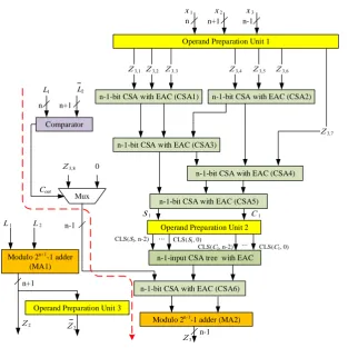
In Figure2,Z3is generated by Operand Preparation
Unit1 (OPU1) withx1,x2 andx3as its inputs. The
values ofZ3,1,Z3,2,Z3,3,Z3,4,Z3,5,Z3,6andZ3,7are
also reduced toS1 andC1 by CSA1, CSA2, CSA3,
CSA4 and CSA5.
Z3is then obtained as
Z3=
(S1+C1)
× 20+ 22+· · ·+ 2n−2 2n−1−1
if L1−L2≥0
(S1+C1)
× 20+ 22+· · ·+ 2n−2
+Z3,8
2n−1−1
Based on Lemma2 Z3=
|ϕ+θ|2n−1−1 if L1−L2≥0
|ϕ+θ+Z3,8|2n−1−1 if L1−L2< 0
(23)
ϕ=
n−2 2 X
i=0
CLS(S1,2i) (24)
θ=
n−2 2 X
i=0
CLS(Ci,2i) (25) where CLS(x,y) equals toy-bit circular left shift ofx. Operand Preparation Unit2 (OPU2) is used to implement Z3 with S1 and C1 as its inputs. Also
OPU2 generates multiple (n−1)-bit outputs. The outputs are CLS(C1, n−2), ..., CLS(C1,0) and CLS
(S1, n−2), ..., CLS(S1,0). To obtain a compact final
output, all of the outputs must be reduced by a CSA tree. So the output of the mentioned CSA tree and the output of the MUX connect to the CSA block and later to the modulo 2n−1−1 adder. The final result
of the MA2 isZ3signal which will be used in the next
step.
Z2is the other signal which should be prepared for
the next step. To Decrease the delay of the proposed design, it is preferred to computeZ2in parallel with
calculatingZ3. Based on the Equation (11),Z2should
be obtained by a modular adder in modulo 2n+1−1
named MA1. Also, ¯Z2 is needed in the second step
of design; therefore, the output of the MA1 goes to Operand Preparation Unit3 (OPU3), includingn+ 1 inverters, to produce ¯Z2. Only in the first step, all of
the above mentioned calculations are done in parallel with computingZ3. Thus the delay of computingZ2
is not considered in the critical path delay. Hardware implementations ofZ2andZ3 are shown in Figure2.
After the calculation ofZ2 andZ3, Y can be
ob-tained from its residues in 3-moduli set Γ as
Y =Z1+Z2P1+Z3P1P2 (26)
Y =Z1+Z2×(2n−1) +Z3×(2n−1)× 2n+1−1
(27) At the next level of design,Z1,Z2, andZ3 are used
with consideration of the value of Y. Furthermore,Z2
andZ3are computed at the first stage for more parallel
architecture. There is no need to compute the final value ofY at the first stage. Only some arrangements of Z1, Z2andZ3 which are needed in computingY
and indicated by yi,i= 1, . . . ,7, are utilized at the next level of design. Therefore the delay of computing Y is omitted. The yi signals are expressed by the
following expression:
Y =Z1+Z2(2n−1) +Z3(2n−1) 2n+1−1
=Z1+Z20· · ·0 | {z }
n
−Z2+Z30· · ·0 | {z } 2n+1
−Z30· · ·0 | {z } n+1
−Z30· · ·0 | {z }
n
+Z3 (28)
Y =y1+y2+y3+y4+y5+y6+y7 (29)
wherey1 =Z1 ,y2 =Z20· · ·0 | {z }
n
,y3=−Z2,y4= Z30· · ·0
| {z } 2n+1
,y5=−(Z30· · ·0 | {z } n+1
) ,y6=−(Z30· · ·0 | {z }
n ) and
y7=Z3.
3.2 Second Step Design
After the computation ofyi,i= 1, . . . ,7, the two mod-ulus superset Λ is considered for obtaining weighted numberX. The residue of weighted numberXin mod-ulo P123 andP4 is equal to Y andx4, respectively,
whereP123= (2n−1)× 2n+1−1× 2n−1−1and P4= 2n. The MRC method for moduli set with two
modulus is utilized to calculateX as follows:
X =v1+v2P123 (30)
where
v1=Y (31)
v2=
(x4−Y) P123−1
P
4 P4
(32)
Proposition 4. The multiplicative inverse ofP123in moduloP4is equal to−2n−1−1.
Proof. According to multiplicative inverses defini-tion, we have:
(2
n−1)× 2n+1−1
× 2n−1−1× P123−1
P
4 2n= 1
→
(2n−1)× 2n+1−1
× 2n−1−1× −2n−1−12n
=(−1)×(−1)× −22n−2+ 1
2n+1−1 =|(−1)×(−1)×1|2n+1−1= 1
thus,
v2=
(x4−Y)×(−1)× 2n−1+ 12n=|Y −x4|2n
(33) By replacing Y based on Equation (29),V2could
be rewritten as:
v2=
y1+y2+y3+y4+y5+y6+y7+ ¯x4+ 1
× 2n−1+ 1
2n
Accord-n-1-bit CSA with EAC (CSA5)
n-1-input CSA tree with EAC
Modulo 2n-1
-1 adder (MA2)
Z 3
Operand Preparation Unit 2
n-1-bit CSA with EAC (CSA4) Operand Preparation Unit 1
x 1 x 2 x 3
Comparator
n-1-bit CSA with EAC (CSA1) n-1-bit CSA with EAC (CSA2)
n-1-bit CSA with EAC (CSA3)
...
CLS(S1, n-2)
CLS(C1, 0)
S 1 C 1
Cout
n-1-bit CSA with EAC (CSA6) Mux
Z 3,8 0 L1 L2
Z 3,7 Z 3,6
Z 3,5 Z 3,4 Z 3,3
Z 3,2 Z 3,1
Modulo 2n+1
-1 adder (MA1)
L 1 L 2
Z 2
Operand Preparation Unit 3
Z 2
...
CLS(S1, 0) CLS(C1, n-2)
n n+1 n-1
n n+1
n-1
n+1
n-1
Figure 2. Hardware schema for first step design
ingly, only the lowest weightednbits are used in the operations. Therefore,v2 can be expressed as:
v
2=
Z
1,00
· · ·
0
| {z }
n−1
+ ¯
Z
2,00
· · ·
0
| {z }
n−1
+
Z
3,0Z
3+¯
x
4,00
· · ·
0
| {z }
n−1
+¯
x
4+
Z
1+ ¯
Z
2+
µ
2n (35)
v2=
K1+K2+Z1+ ¯Z2+µ
2n (36) where
k1=XORhx¯4,0,x¯4,n−1ix¯4,n−2· · ·x¯4,1¯x4,0 (37)
k2=XOR
Z1,0,Z¯2,0, Z3,0
Z3 (38) µ= 0· · ·00
| {z } n−2
10 (39)
The structure of the OPU4 is implemented based on the above equation forv2. The inputs areZ1,Z2,Z3,
andx4 and its outputs arek1andk2. CSA7 neglects
the nth bit of its outputs. CSA7 is also put a 0 in the least significant bit of the carry. It also omits the most significant bit of ¯Z2by considering Equation (29)
based on the previous subsection. This procedure is also done by CSA8 and CSA9. Finally, the outputs of the CSAs go to the Modular adder 3 (MA3) as its
n-bit CSA(CSA7)
n-bit CSA(CSA8)
Modulo 2n adder (MA3)
v2
k1 k2
Z2
Z1
n-bit CSA(CSA9) µ
Operand Preparation Unit 4
x4 Z1 Z2 Z3
Figure 3. Calculation of ofv2
inputs to computev2. Hardware implementation of v2is shown in Figure3.
X=v1+v2×(2n−1)× 2n+1−1× 2n−1−1
(40) Sincev1=Y,v1is replaced byY as follow: X=Y +v2×(2n−1)× 2n+1−1
× 2n−1−1
(41) Equation (41) can be simplified as
X =v2Z3Z2Z1−0· · ·0 | {z } n−1
v20· · ·0 | {z } 2n+1
−0· · ·0 | {z }
n
v2Z3Z2
−0· · ·0 | {z } n+1
v2Z3v2+v20· · ·0 | {z } n+1
+v20· · ·0 | {z }
n
+v2Z3 (42)
X =v2Z3Z2Z1+ 1· · ·1 | {z } n−1
¯
v21· · ·1 | {z } 2n+1
+ 1· · ·1 | {z } n+1
¯
v2Z¯3Z¯2
+ 1· · ·1 | {z }
n ¯
v2Z¯3v¯2+v20· · ·0 | {z } n−1
11 +v20· · ·0 | {z }
n
+v2Z3
(43)
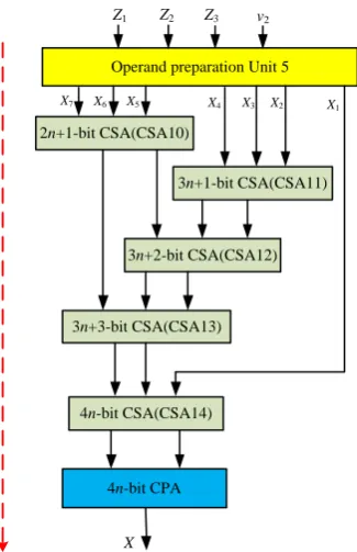
X is the summation of seven values,
7 P
k=1 Xk , where X1 = v2Z3Z2Z1 , X2 = 1· · ·1
| {z } n−1
¯
v21· · ·1 | {z } 2n+1
,
X3 = 1· · ·1 | {z } n+1
¯
v2Z¯3Z¯2 , X4 = 1· · ·1 | {z }
n ¯
v2Z¯3v¯2 , X5 = v20· · ·0
| {z } n−1
11 ,X6=v20· · ·0 | {z }
n
andX7=v2Z3.Xk with the bit-length of 4n-bit enters to the carry save adder tree and the outcomes of carry save adder connect to the input of a 4n-bit CPA to compute weighted number X. Figure4depicts the architecture of this scenario.
X
v2
Operand preparation Unit 5
Z1 Z2 Z3
4n-bit CPA
X1
X2
X3
X4
X5
X6
X7
2n+1-bit CSA(CSA10)
3n+1-bit CSA(CSA11)
3n+2-bit CSA(CSA12)
3n+3-bit CSA(CSA13)
4n-bit CSA(CSA14)
Figure 4. Hardware implementation for calculation ofX
3.3 Numerical Example
Considering moduli set{63, 127, 31, 64}, which is derived from moduli set Ψ whenn= 6, the RNS num-ber (33, 7, 5, 63) can be converted to its equivalent in weighted numberX as:
First stage:
x1= 3310= 1000012 x2= 710= 00001112 x3= 510= 001012
By substituting these values in Equation (6),(11), (19) and (21), the following results will be obtained:
Z1= 3310= 1000012 L1= 10000102 L2= 00011102 Z2= 01101002 Z3= 110012
Second stage: by considering Equation (31), (36) and (43), the desired values in second step are ob-tained:
v1=Y = 10732210= 110100011001110102 k1= 0
k2= 5710= 1110012 v2= 3910= 1001112
X = 107322 + 39×63×127×31 = 9876543 ThusX = 9876543, and the verification can be sim-ply done as
x1=|9876543|63= 33 x2=|9876543|127= 7 x3=|9876543|31= 5 x4=|9876543|64= 63
4
Hardware Cost and the Delay of
Pro-posed Converter
Table 2. Different conditions of a full adder cell according on constant input
Number of constant value Constant value Reduced gates
1 1 a pair of two input XNOR and OR gate
1 0 a pair of two input XOR and AND gate
2 Same value ( both 0 or both 1) Wire
2 Same value ( one input 0 another 1) Inverter gate
which two numbers are aggregated in a ripple structure. The logic function of a full adder is described by the following equations:
Sum=XOR(x, y, z) =xyz+xy¯z¯+ ¯xyz¯+ ¯xyz¯ (44)
Carry=xy+xz+zy (45) According to Equations (44) and (45), if one of the inputs of the full adder equals to 1 (for instancez= 1), the SumandCarry are equivalent toxy+ ¯xy¯and
x+yrespectively. If one of the inputs equals to 0 (for instancez = 0), theSumandCarry are equivalent toxy¯+ ¯xyandxyrespectively. In these two cases only two input gates are used. If two inputs have constant values, the simplification process is the same as above. Table2shows different conditions of a full adder cell according to constant inputs.
In the first step of the design of the reverse converter, the modular adders (MA1, MA2) are implemented by CPAs with EAC (Figure2). The 2k−1 modular adder has the similar area and double delay compared to thek-bit CPA. The latter modular adder (MA3) is implemented by a regularn-bit CPA neglecting its carryout (Figure3). CSAs used in the design of the reverse converter are divided to the regular CSA and CSA with EAC [13].
(1) In the first level of design, CSAs of the reduction tree are CSAs with EAC. The output of a final CSA enters to the modulo 2n−1−1 adder (MA2). (2) The summation of five operands in modulo 2n
computesV2in the initiation of the second step
of design. The structure of the reduction tree used for computing V2 employs three regular
CSAs. Due to the fact that the output of the reduction tree must be in modulo 2n, for achiev-ing the hardware cost efficiency, the carryout signal of every CSA in the architecture shown in Figure3is neglected.
(3) In the last part of the second step of design, for computingX, CSAs which their inputs are signals with different bit numbers, are used. The only difference between regular CSA and CSA with EAC is the generated result ofcfrom CSA.
Fig-ure5demonstrates basic architecture of a CSA and a CSA with EAC. The delay of n-bit CSA denotes additional time of a full adder cell. In CSA like CPA, hardware cost can be reduced according to the con-stant input values. In general, the hardware cost of
n-bit CSA is equal to the hardware cost ofnfull adder cell. Table3shows the hardware cost and the delay of various components in the proposed reverse converter.
5
Comparison
This section presents the comparison of the pro-posed reverse converter architecture for the mod-uli set Ψ with other balanced 4-modmod-uli sets with the same dynamic range class, such as the 4-moduli sets {2n−1,2n,2n + 1,2n+1−1
[13, 14],{2n−1,2n,2n + 1,2n+1+ 1 [13, 15],
{2n−3,2n−1,2n+ 1,2n+ 3}[16] and{2n,2n+1−
1,2n−1,2n−1−1 [17]. The comparisons are done
in terms of the delay and the area of the reverse converter. Table4shows the comparison between the proposed reverse converter and its other state-of-the-art counterpstate-of-the-art. In order to achieve fair comparison, the delay and the area of the modulus adders and carry save adders are considered the same as [24].As shown in Table2, the proposed reverse converter for the moduli set Ψ has achieved the highest speed of the reverse converter compared to{2n−1,2n,2n+ 1,2n+1−1 [13,14],{2n−1,2n,2n+ 1,2n+1+ 1 [13, 15], {2n−3,2n −1,2n + 1,2n+ 3} [16] and
{2n,2n+1 −1,2n −1,2n−1−1 [17]. It is worth mentioning that, the proposed reverse converter is the fastest adder based reverse converter in the balanced 4-moduli class [17].
x0 x1 x2 xn-2
yn-1
y0 y1 y2 yn-2
yn-1
z0 z1 z2 zn-2
zn-1
s0 s1 s2 sn-2
sn-1
...
...
c0 c1 c2
cn-1 cn-2 ... 0
α
β
Generate Sum and Carry from
α,β and operands
Carry Save Adder z y x
s c s
c x+y+z=2c+s
(a)
x0 x1 x2 xn-2
yn-1
y0 y1 y2 yn-2
yn-1
z0 z1 z2 zn-2
zn-1
s0 s1 s2 sn-2
sn-1
...
...
c0 c1 c2
cn-2 ...
Carry Save Adder with End Around Carry
z y x
s c s
c cn-1
(b)
Figure 5. Basic Architecture for (a) a Carry Save Adder and (b) a CSA with End Around Carry.
Table 3. Hardware and delay of various components in the proposed reverse converter.
Component Area Delay Component Area Delay
OPU1 (2n+ 1)AInv 1DInv CSA7 nAF A 1DF A
Comparator 3nAAN D+nAOR3 nDAN D CSA8 (n−1)AF A+AXOR 1DF A
+nDOR3 +AAN D
CSA1 1AF A 1DF A CSA9 (n−2)AXOR+ 1AXN OR 1DInv
+ (n−2) (AXN OR+AOR) + (n−2)AAN D+ 1AOR
CSA2 2AF A 1DF A MA3 (n−3)AF A (n−3)DF A
+1AXOR+ 1AAN D +1DHA
CSA3 (n−1)AF A 1DF A OPU5 (2n−1)AInv 1DInv
CSA4 (n−1)AF A 1DF A CSA10 (n−2)AF A 1DF A
+2AXOR+ 2AAN D
CSA5 (n−1)AF A 1DF A CSA11 (n−2)AF A 1DF A
+ (2n+ 2) (AXN OR+AOR)
OPU2 0 0 CSA12 2nAF A 1DF A
+ (n+ 1) (AXOR+AAN D)
CSA Tree n2−n
AF A pDF A CSA13 2nAF A 1DF A
+ (n+ 1) (AXOR+AAN D)
CSA6 (n−2)AF A 1DF A CSA14 (3n+ 1)AF A 1DF A
+AXOR+AAN D +2 (AXOR+AAN D)
MA1 (n+ 1)AF A (2n+ 2)DF A CPA (4n−2)AF A (4n−2)DF A
+2 (AXOR+AAN D) +1DHA
MA2 (n−1)AF A (2n−2)DF A MUX 2:1 0 0
Table 4. Hardware requirements and delay of reverse converters.
Moduli Set Design Hardware requirements Delay
2n−1,2n,2n+ 1,2n+1−1 [13]−1 (9n+ 5 + ((n−4) (n+ 1)/2))A
F A (23n+ 12)/2DF A
+ 2nAXN OR+ 2nAOR+ (6n+ 1)AIN V
2n−1,2n,2n+ 1,2n+1+ 1 [13] 2n2+ 11n+ 3 11.5nD
F A
2n−1,2n,2n+ 1,2n+1+ 1 [13]−2 (6n+ 7)A
IN V + n2+ 12n+ 12AF A (16n+ 22)DF A
+2n(AXN OR+AOR) + (4n+ 8)A2:1M U X
2n−1,2n,2n+ 1,2n+1+ 1 [15] (58n+ 23 +log
2(c+ 1))AF A 24n+ 17 + logc2+1
DF A
{2n−3,2n−1,2n+ 1,2n+ 3} [16]-C1CE 25.5n+ 12 + 2.5n2
AF A (18n+ 23)DF A
+5nAHA+ 3n(AXN OR+AOR)
{2n−3,2n−1,2n+ 1,2n+ 3} [16]-C2CE (20n+ 17)A
F A+ (3n−4)AHA (13n+ 22)DF A
+2n(5n+ 2)A
ROM +3DROM
{2n−3,2n−1,2n+ 1,2n+ 3} [16]-C3CE (23n+ 11)A
F A+ (2n− 2)AHA (16n+ 14)DF A
+(6n+ 4)2nA
ROM +DROM
2n−1,2n,2n+ 1,2n+1−1 [14]-3stage-CE (n2+ 10n+ 3)A
F A+AHA (9n+ 6 +m)DF A∗
+(3n+ 2)AIN V + 2A2:1M U X
2n,2n+1−
1,2n−1,2n−1−
1 [17]-D1-C-I n2+ 16n+ 6
AF A+ 4nAIN V (12n+ 9 +q)DF A∗
+ (n+ 2) (AXN OR+AOR)
+ (3n−5) (AXOR+AAN D)
2n,2n+1−1,2n−1,2n−1−1 [17]-D1-C-III n2+ 24n+ 24AF A+ (2n+ 3)AHA (8n+ 11 +q)DF A∗
+2(AXN OR+AOR)
+ (2n−5) (AXOR+AAN D)
+ (2n+ 1)A3:1M U X+ 4nAIN V
2n,2n+1−
1,2n−1,2n−1−
1 [17]-D1-C-II n2+ 22n+ 22
AF A+ (2n+ 2)AHA (8n+ 11 +q)DF A∗
+10(2n+ 1)AROM+ 2 (AXN OR+AOR)
+ (2n−5) (AXOR+AAN D)
+(2n+ 1)A2:1M U X+ 4nAIN V
2n,2n+1−
1,2n−1,2n−1−
1 Proposed n2+ 21n−11
AF A (7n+ 1)DF A
+ (3n+ 1) (AXN OR+AOR) +n(DOR3+DAN D)
+ (6n+ 9)AAN D+ (3n+ 9)AXOR +2DHA+ 4DIN V
+nAOR3+ (5n+ 1)AIN V
∗mandqare the number of levels in CSA tree with (n+ 2), (n+ 1) inputs, respectively.
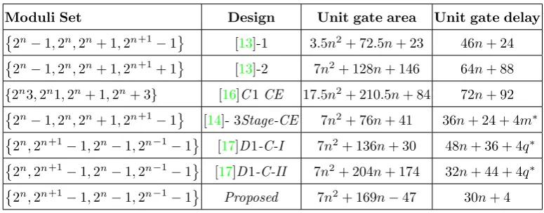
which confirms the remarkable improvement in terms of speed of the reverse converter. Also degraded hard-ware resources are achieved compared to [13–17].
6
Conclusion
In this paper, the quadruple moduli set Ψ was the fo-cus of study in reducing the computational intensity of the reverse converter design. Ψ has the dynamic range of 4n and utilizes modulos only in the form of 2k−1beside modulo 2n, which provides efficient
arithmetic operations in RNS channels. The new re-verse converter eliminates the extra intermediate cal-culations. For each level of design, the moduli subsets are selected to make the design more efficient in both delay and the hardware cost. To put everything in the nutshell, the overall area and time complexity analy-sis indicates that the proposed reverse converters are more efficient than the converters for the 4-moduli set
Table 5. Unit gate area and delay of reverse converters.
Moduli Set Design Unit gate area Unit gate delay
2n−1,2n,2n+ 1,2n+1−1 [13]-1 3.5n2+ 72.5n+ 23 46n+ 24
2n−1,2n,2n+ 1,2n+1+ 1 [13]-2 7n2+ 128n+ 146 64n+ 88
{2n3,2n1,2n+ 1,2n+ 3} [16]C1CE 17.5n2+ 210.5n+ 84 72n+ 92
2n−1,2n,2n+ 1,2n+1−1 [14]- 3Stage-CE 7n2+ 76n+ 41 36n+ 24 + 4m∗
2n,2n+1−1,2n−1,2n−1−1 [17]D1-C-I 7n2+ 136n+ 30 48n+ 36 + 4q∗
2n,2n+1−1,2n−1,2n−1−1 [17]D1-C-II 7n2+ 204n+ 174 32n+ 44 + 4q∗
2n,2n+1
−1,2n−1,2n−1
−1 Proposed 7n2+ 169n−47 30n+ 4
∗mandqare the number of levels in CSA tree with (n+ 2), (n+ 1) inputs, respectively.
Acknowledgements
The authors are grateful to the anonymous reviewers’ valuable comments and suggestions that improved the quality of manuscript. Also the authors would like to thank Dr. B. Yoberd and Ms. F. Shaker for their literature contributions.
References
[1] MA Bayoumi and P Srinivasan. Parallel arith-metic: from algebra to architecture. InCircuits and Systems, 1990., IEEE International Sympo-sium on, pages 2630–2633. IEEE, 1990.
[2] T Stouraitis and V Paliouras. Considering the alternatives in low-power design. Circuits and Devices Magazine, IEEE, 17(4):22–29, 2001. [3] Behrooz Parhami. Computer arithmetic:
algo-rithms and hardware designs. Oxford University Press, Inc., 2009.
[4] Mi Lu.Arithmetic and logic in computer systems, volume 169. John Wiley & Sons, 2005.
[5] Richard Conway and John Nelson. Improved rns fir filter architectures. Circuits and Systems II: Express Briefs, IEEE Transactions on, 51(1): 26–28, 2004.
[6] Ricardo Chaves and Leonel Sousa. Rdsp: A risc dsp based on residue number system. InDigital System Design, 2003. Proceedings. Euromicro Symposium on, pages 128–135. IEEE, 2003. [7] Wei Wang, MNS Swamy, and M Omair
Ah-mad. Rns application for digital image process-ing. InSystem-on-Chip for Real-Time Applica-tions, 2004. Proceedings. 4th IEEE International Workshop on, pages 77–80. IEEE, 2004.
[8] Sung-Ming Yen, Seungjoo Kim, Seongan Lim, and Sang-Jae Moon. Rsa speedup with chinese re-mainder theorem immune against hardware fault cryptanalysis. Computers, IEEE Transactions
on, 52(4):461–472, 2003.
[9] Mohammad Esmaeildoust, Dimitrios Schini-anakis, Hamid Javashi, Thanos Stouraitis, and Keivan Navi. Efficient rns implementation of el-liptic curve point multiplication over.Very Large Scale Integration (VLSI) Systems, IEEE Trans-actions on, 21(8):1545–1549, 2013.
[10] Javier Ram´ırez, Antonio Garc´ıa, U Meyer-Baese, and A Lloris. Fast rns fpl-based communications receiver design and implementation. In Field-Programmable Logic and Applications: Reconfig-urable Computing Is Going Mainstream, pages 472–481. Springer, 2002.
[11] Keivan Navi, Amir Sabbagh Molahosseini, and Mohammad Esmaeildoust. How to teach residue number system to computer scientists and engi-neers. Education, IEEE Transactions on, 54(1): 156–163, 2011.
[12] MohammadReza Taheri, Elham Khani, Moham-mad Esmaeildoust, and Keivan Navi. Effi-cient reverse converter design for five moduli set
{2n,22n+1−1,2n/2−1,2n/2+1,2n+1}.Journal of Computations & Modelling, 2(1):93–108, 2012. [13] PV Ananda Mohan and AB Premkumar. Rns-to-binary converters for two four-moduli sets{2 n-1, 2 n, 2 n+ n-1, 2 n+ 1- 1}and{2 n- 1, 2 n, 2 n+ 1, 2 n+ 1+ 1}. Circuits and Systems I: Regular Papers, IEEE Transactions on, 54(6):1245–1254, 2007.
[14] B Cao, T Srikanthan, and CH Chang. Efficient reverse converters for four-moduli sets {2n- 1, 2n, 2n+ 1, 2n+ 1- 1}and{ 1, 2n, 2n+ 1, 2n-1- 1}. IEE Proceedings-Computers and Digital Techniques, 152(5):687–696, 2005.
[16] PV Ananda Mohan. New reverse converters for the moduli set{2n-3, 2n-1, 2n+ 1, 2n+ 3}. AEU-International Journal of Electronics and Commu-nications, 62(9):643–658, 2008.
[17] Mohammad Esmaeildoust, Keivan Navi, Moham-madReza Taheri, Amir Sabbagh Molahosseini, and Siavash Khodambashi. Efficient rns to bi-nary converters for the new 4-moduli set{2n, 2n+ 1-1, 2n-1, 2n-1-1}. IEICE Electronics Express, 9 (1):1–7, 2012.
[18] Lampros Kalampoukas, Dimitris Nikolos, Costas Efstathiou, Haridimos T Vergos, and John Kala-matianos. High-speed parallel-prefix modulo 2n-1 adders. IEEE Transactions on Computers, (7): 673–680, 2000.
[19] Costas Efstathiou, Haridimos T Vergos, and Dim-itris Nikolos. Fast parallel-prefix modulo 2 n+ 1 adders. Computers, IEEE Transactions on, 53 (9):1211–1216, 2004.
[20] Riyaz Patel, Mohammed Benaissa, Neil Powell, Said Boussakta, et al. Novel power-delay-area-efficient approach to generic modular addition. Circuits and Systems I: Regular Papers, IEEE Transactions on, 54(6):1279–1292, 2007. [21] W Kenneth Jenkins and Benjamin J Leon. The
use of residue number systems in the design of finite impulse response digital filters. Circuits and Systems, IEEE Transactions on, 24(4):191– 201, 1977.
[22] Mohammad Esmaeildoust, Keivan Navi, and Mo-hammadReza Taheri. High speed reverse con-verter for new five-moduli set {2n, 22n+ 1-1, 2n/2-1, 2n/2+ 1, 2n+ 1}. IEICE Electronics Ex-press, 7(3):118–125, 2010.
[23] NAVI Keivan, Mohammad Esmaeildoust, and Amir Sabbagh Molahosseini. A general reverse converter architecture with low complexity and high performance. IEICE TRANSACTIONS on Information and Systems, 94(2):264–273, 2011. [24] Amir Sabbagh Molahosseini, Keivan Navi, Chitra
Dadkhah, Omid Kavehei, and Somayeh Timarchi. Efficient reverse converter designs for the new 4-moduli sets and based on new crts. Circuits and Systems I: Regular Papers, IEEE Transactions on, 57(4):823–835, 2010.
MohammadReza Taherireceived his B.Sc. in Computer Hardware Engineering from Is-fahan University, IsIs-fahan, Iran. He obtained his M.Sc. degree in Computer System Archi-tecture from Science and Research Branch of Islamic Azad University, Tehran, Iran. He is currently pursuing his Ph.D. Degree in Com-puter Architecture at Shahid Beheshti Uni-versity, Tehran, Iran. He is also a member of the Nanotechnology and Quantum Computing Laboratory of Shahid Beheshti University since 2009. His current research interests include residue number system, low power arithmetic, approximate computing, and circuit techniques for emerging technologies.
Nasim Shafieereceived the B.Sc degree in computer hardware engineering from Shahid Beheshti University, Tehran, Iran in 2014. She is a member of the Nanotechnology and Quantum Computing Laboratory of Shahid Beheshti University since 2013. Her research interests include low power computer arithmetic, approximate computing, and robotic.
Mohammad Esmaeildoust received his M.Sc. degree in Computer architecture at Shahid Beheshti University of Technology, Tehran, Iran, in 2008. He also received the Ph.D. degree in computer architecture from Shahid Beheshti University of Technology, Tehran, Iran, in 2012. He is currently As-sistant Professor in faculty of Marine Engi-neering, Khorramshahr University of Marine Science and Technology. His research interests include VLSI design, Cryptography, Network security, computer arithmetic.
Zhale Amirjamshidiearned her M.Sc. in electronic engineering from Central Branch of Islamic Azad University, Tehran, Iran. She is currently pursuing the Ph.D. degree in electronic engineering at Iran University of Science and Technology, Tehran, Iran. Her research interests are mainly focus on low power digital arithmetic and renewable energy.
Reza Sabbaghi-nadooshan received his B.Sc. and M.Sc. in electrical engineering from the Iran University of Science and Technology, Tehran, Iran, in 1991 and 1994 and Ph.D. in Electrical Engineering from the Science and Research Branch, Islamic Azad University, Tehran, Iran in 2010. From 1998, he became faculty member of Department of Electronics in Central Tehran branch, Islamic Azad University, Tehran, Iran. His current research interests include nanocomputing and networks-on-chips. He is a member of IEEE.