A Large Range Multi-Axis Capacitive Force/Torque
Sensor Realized in a Single SOI Wafer
D. Alveringh, R.A. Brookhuis, R.J. Wiegerink, G.J.M. Krijnen, M.J. de Boer and P.E. Veltink
Transducer Science and Technology Group, MESA+ Institute for Nanotechnology, University of Twente,
P.O. Box 217, 7500 AE Enschede, The Netherlands
Abstract—A MEMS-based silicon capacitive force/torque
sen-sor is designed and realized to be used for biomechanical applications and robotics. The sensor is able to measure the forces in three directions and two torques using four parallel capacitor plates and four comb-structures. Novel spring and lever structures are designed to separate the different force components and minimize crosstalk. The fabrication process is based on deep reactive ion etching on both sides of a single silicon-on-insulator wafer and uses only two masks making it very suitable for mass production. The sensor has a force range of 2 N in shear and normal direction and a torque range of more than 6 N mm. It has a high sensitivity of 38 fF N−1 and 550 fF N−1 in shear and
normal direction respectively. A calibration matrix is derived from the sensor’s measured characteristics.
I. INTRODUCTION
M
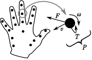
INIATURIZED multi-axis force/torque sensors are widely used in medical applications, tactile sensing and robotics. Many prostheses, for example, require safe and com-fortable interaction with people who underwent amputation of a part of a limb. Bad fitting between the socket of the prosthesis and the residual limb may cause pain and even damage to the underlying blood vessels [1], [2]. Measuring the shear forces and normal forces between the socket and the residual limb is possible with multiple small force sensors. The prosthesis can use this information to adjust the shape of the socket, making the load distribution as comfortable and healthy as possible.Other applications are in the field of characterization of the human body. For example, power measurements of the human hand are important for rehabilitation purposes or the optimization of the endurance of athletes [3]. These power measurements can be done with force/torque sensors, ac-celerometers and gyroscopes at each joint integrated in a glove (figure 1).
F
v
ω
T
[image:1.612.102.249.616.712.2]P
Fig. 1. Power measurements of the human hand using force sensors,
accelerometers and gyroscopes. The power P in one element is equal to
~
F·~v+T~·~ω.
Force sensors are also very interesting for robotics. Hu-manoid robots [4] or robotic hands [5] have to interact with the environment. Force sensors on top of the fingers and toes help the robot to measure load distributions on the hands and feet. Even the difference between rough and flat surfaces may be sensed by the robot.
For the three mentioned applications, a few specific require-ments are applicable:
• the sensor should measure multiple (preferably six)
de-grees of freedom;
• the sensor is small, preferably less than 1 cm2 with a
thickness of less than 1 mm;
• the sensor should be able to handle human forces, i.e. at
least a few newtons.
Commercially available non-MEMS load cells support high force ranges, but are often too large to integrate in the applications mentioned above. There are MEMS-based force and torque sensors available in literature, but many lack the support for measuring torques [6], [7] or forces [8]. Besides, many sensors only support forces in the milli newton or micro newton range [9], [10], [11]. The fabrication process of most MEMS-based sensors is still in an experimental stage [6], [7], [11], [12], [13], they use non-trivial polymer technologies or crucial wafer bonding steps in the process. This makes the existing force sensors even less attractive, since above specified applications need tens of these expensive sensors per device.
However, a few force/torque sensors with piezoresistive readout satisfy most of the requirements. But sensors with capacitive readout have a better temperature performance, lower drift and higher sensitivity [14]. We present a miniature easy to fabricate multi-axis capacitive force/torque sensor with a large range. The sensor is initially developed for quantitative measurement of the interaction forces and torques between human fingers and the environment as a cheaper alternative for the sensor of Brookhuis et al. [13] But given its large force range and small dimensions, the sensor can also be used for other biomechanical applications or robotics.
II. DESIGN
present in the device layer and results in a differential change in gap between the comb-fingers (figure 2).
Cx,− Cx,+
(a) In rest position.
Fx
↑Cx,−
↓Cx,+
[image:2.612.55.294.97.173.2](b) With load in x-direction.
Fig. 2. Principle of operation for shear forces.
A normal force results in an out-of-plane displacement, which is measured by parallel plate electrodes (figure 3(b)). By differential measurement of two opposite electrodes (figure 3(c)), the applied torque is determined.
Cz,11 Cz,22
(a) In rest position.
Fz
↓Cz,11 ↓Cz,22
(b) With load in z-direction.
Tx
↑Cz,11 ↓Cz,22
[image:2.612.329.543.158.250.2](c) With torque around x-axis.
Fig. 3. Principle of operation for normal forces and torques.
A. Mechanics of the suspended core
Capacitive force/torque sensors are based on measuring a displacement. A system of springs convert the force to a displacement. Ideal springs obey Hooke’s law.
F =k·u, (1)
T =c·φ, (2)
with F the force, k the stiffness and u the displacement, T the torque, c the rotational stiffness andφ the angle. The system of springs is dimensioned for forces in the first place, therefore, it is necessary to know the stiffness in each direction. The proposed force/torque sensor uses the point symmetric v-shaped spring system shown in figure 4.
Fig. 4. A six degrees of freedom stage using folded sheet springs. The
combination of three folded sheet springs is called a spring triplet.
The stiffness of the stage is equal for all shear directions [15]. The stage is initially only compliant for in-plane trans-lations. By reducing the thickness of the sheets compared to the length and width of the sheets, the stage can be made compliant for normal direction and torques too. To increase stiffness in all directions, multiple spring triplets are added as is illustrated in figure 5.
L
W
L
[image:2.612.58.294.267.407.2]N3s
Fig. 5. The point symmetric v-shaped spring system and the parameters of
each spring realized in the handle layer with thicknessT.
The stiffness in shear directions is equal to:
kx=
45N3sEIx
2L3 , (3)
with kx the stiffness in x-direction, N3s the number of
spring triplets, E Young’s modulus, Ix the second moment
of area in x-direction andLthe length of one spring part. The stiffness in normal direction is derived from the guided beam theory from [16]:
kz=
12(3N3s)EIz
(2L)3 , (4)
with kz the stiffness in z-direction and Iz the second
moment of area in z-direction. The second moments of area are as follows.
Ix=
T W3
12 , (5)
Iz=
W T3
12 , (6)
withT the thickness of the beam (equal to the thickness of the handle layer) andW the width of the beam.
The six degrees of freedom stage can be tuned for trans-lations with parameters L, W and N3s by substituting the
equations of 5 in equations 3 and 4:
kx∝
N3s
L3 W 3,
(7)
kz∝
N3s
L3 W. (8)
[image:2.612.126.222.644.721.2]length L to be larger. Table I shows the chosen dimensions for the proposed force/torque sensor.
TABLE I
DIMENSIONS OF THE SUSPENDED CORE.
Quantity Symbol Value
Length of one spring part L 480 µm
Width of the spring W 108 µm
Thickness of the spring T 400 µm
Number of spring triplets N3s 5
Diameter of the core Dcore 2.5 mm
Diameter of the sensor Dsensor 9.24 mm
Stiffness in shear direction kx 7.2·106N m−1
Stiffness in normal direction kz 1.9·107N m−1
B. Simulations of the suspended core
To verify the mathematical model and obtain an impression of the stress in the device, finite element method (FEM) sim-ulations were done using COMSOL Multiphysics 4.3.0.151. The suspended core was drawn using computer aided design (CAD) software with the dimensions of table I. All structures have rounded corners (see figure 5) for two reasons:
• it reduces the maximum stress because the beams are
thicker at places where the deformation would be origi-nally higher;
• the etching process does not allow very sharp corners. By
using round corners in the simulations, the simulations become more true to nature.
The simulations were done for a shear force of 10 N, a normal force of 10 N and a torque around a shear axis of 10 N mm. Table II shows the simulation results.
TABLE II FEMSIMULATION RESULTS.
Quantity Symbol Value
Stiffness in shear direction kx 8.9·106N m−1
Maximum stress forFx= 10 N σmax,x 8.5 GPa
Stiffness in normal direction kz 1.2·107N m−1
Maximum stress forFz= 10 N σmax,z 4.0 GPa
Rotational stiffness around shear axes cx 41 N m rad−1
Maximum stress forTx= 10 N mm σmax,φ 0.92 GPa
The found stiffnesses are slightly different than the model predicts. This may be because of the rounded corners. The found stresses for the simulated forces and torques are quite high for silicon; it can be concluded that the sensor’s maximum range for force and torque will be in the order of newtons and newton millimeters respectively.
C. Capacitive measurement
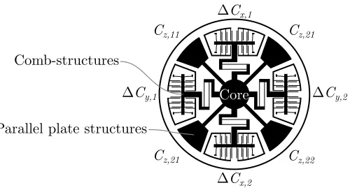
The sensor uses capacitive sensing structures. Figure 6 shows where the capacitors are located. There are large parallel electrode capacitors for normal force and torque measurements and comb-structures for shear force measurements. Both ca-pacitor structures can be modeled as gap closing parallel plate capacitors [17]:
C(u) =Npε
A d0−u
→C(F) =Npε kA
kd0−F
. (9)
ΔCx,1
ΔCx,2
ΔCy,2
ΔCy,1
Cz,11 Cz,21
Cz,21 Cz,22
Comb-structures
Core
[image:3.612.315.565.57.193.2]Parallel plate structures
Fig. 6. Design of the device layer with declaration of all sensing capacitors.
WithCthe capacitance,Npthe number of parallel plates or
finger pairs, εthe absolute permittivity (in this case equal to the dielectric constantε0),Athe overlapping area of one plate
or finger pair,d0 the distance between the plates or fingers in
rest, u the displacement in the same direction as d0, k the
stiffness in the same direction as d0 and F the force in the
same direction asd0.
Normal forces are measured non-differentially using the parallel plate capacitor structures. For small forces, the closing gap capacitor model can be linearized using the Maclaurin series:
Cz(Fz)≈ 1
X
n=0
Cz(n)(Fz)
n! F n z =
Np,zǫAz
d2 0,zkz
Fz+Cz(0). (10)
All parameters can be put in factorβz:
Cz(Fz)≈βzFz+Cz(0), with βz=
Np,zǫAz
d2 0,zkz
. (11)
C(F)is an expression for the total capacitance between two plates or two combs. As can be seen in the sensing structures in figure 6 and in the operating principles in figure 2, shear forces are measured differentially. The differential capacitance
∆Cx is defined as:
Cx,± =Cx,rest±Cx→∆Cx=
Cx,+−Cx,−
2 , (12)
i.e. the actual difference in capacitance due to displacement of one side, which can be measured by calculating half of the difference of the two measured structures (i.e. two plates or two combs). For small forces, the differential closing gap capacitor model may be linearized using the Maclaurin series:
Cx(Fx)≈ 1
X
n=0
∆Cx(n)(Fx)
n! F
n
x (13)
=βxFx, with βx=
Np,xǫAx
d2 0,xkx
. (14)
Fx Fy Fz Tx Ty Tz =K
∆Cx,1 ∆Cx,2 ∆Cy,1 ∆Cy,2
Cz,11
Cz,12
Cz,21
Cz,22
, with K∈R6×8 (15)
The elements in calibration matrix K will be found by measurements and will be reviewed in the discussion.
D. Comb-structures in the device layer
The comb-structures consist of combs mounted on a one degree of freedom stage which is supported by eight single flexures. Spring and lever structures are used to separate the different force components of the suspended core into comb-structure movements (figure 7). This transmission has (for small displacements) very high stiffness in x-direction and therefore transfers the full x-displacement from the core to the comb-structures. In z-direction, the stiffness of the transmis-sion springs are more than 80 times lower than the springs of the comb-structures, so less than 2 % of the z-displacement of the core is transferred to the comb-structures. In y-direction, the stiffness of the transmission springs are negligible com-pared to the the springs of the comb-structures making the comb-structures almost insensitive for y-displacements. In this way, crosstalk between the different force components is mechanically minimized.
u
xu
x4
1
2
3
3
(a) Shear force in x-direction.
u
y4
1
2
3
3
(b) Shear force in y-direction.
u
z4
1
2
3
3
[image:4.612.334.548.57.160.2](c) Normal force in z-direction.
Fig. 7. Transmission (2) from core (1) to comb-structures (4). There are
bumps (3) to prevent snapping of the fingers due to overloading.
All comb-structures have protection against snapping due to overloading: the stage will hit the bumps in figure 7 first before the fingers of the stage will snap to the fingers of the stator, as the distance between the finger pairs is 7 µm and the distance between the bumps and the stage is 5 µm.
The shear displacements are measured differentially. The stator consists of two symmetric electrically isolated parts (figure 8). Displacement of the stage results in an increasing gap at one half of the comb-structures and a decreasing gap at the other half of the comb-structures.
↓
C
x,+↑
C
x,−F
x(a) Differential capacitance change when loaded.
W
fingerd
0d
1 [image:4.612.87.300.65.162.2](b) Close-up of the finger struc-tures with dimensions.
Fig. 8. Electrical design of the comb-structures.
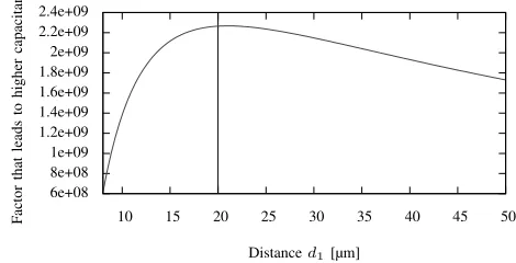
The asymmetric positioning (d1/d0-ratio in figure 11(b)) of
the shuttle-fingers between the stator-fingers is optimized, for a smallerd1/d0-ratio allows more finger structures but increases
the parasitic capacitance and a larger d1/d0-ratio decreases
the parasitic capacitance but takes mores space. The curve in figure 9 is derived from equation 9, its maximum is where:
∂ ∂d1
1
d0+d1+ 2Wf inger
1 d0 − 1 d1
= 0. (16)
The fingers have a width Wf inger of 7 µm. The minimum
distance between the fingers is 7 µm which is used for d0.
Choosing ∼ 20µm for d1 leads to maximum capacitance
change. All parameters are summarized in table III.
6e+08 8e+08 1e+09 1.2e+09 1.4e+09 1.6e+09 1.8e+09 2e+09 2.2e+09 2.4e+09
10 15 20 25 30 35 40 45 50
F actor that leads to higher capacitance
[image:4.612.320.555.399.519.2]Distanced1[µm]
Fig. 9. Optimization of the finger distances: choosingd0 the maximum of
the function will consequent in the highest capacitance.
TABLE III
PARAMETERS OF THE COMB-STRUCTURES.
Quantity Symbol Value
Number of finger pairs Np, x 149
Average overlapping area per finger pair Ax 1.2·10−8m2
Distance between fingers d0 7 µm
Distance between finger pairs d1 20 µm
Width of a finger Wf inger 7 µm
Average length of a finger Lf inger 240 µm
Thickness of a finger Tdevice 50 µm
E. Parallel plate structures in the device layer
capacitance of the comb-structures. The plate is electrically connected to the bond pad with springs that are compliant in all directions. In figure 10, one of the normal sensing structures is shown.
1
3
3
2
5
4
4
[image:5.612.143.205.113.241.2]3
3
Fig. 10. Capacitor plate (2) is directly coupled with the core (1). Wires (4)
connect the capacitor plate to the bond pand (5) and have no effect on the mechanics due to there folds. There are bumps (3) to prevent snapping of the plates due to shear overloading.
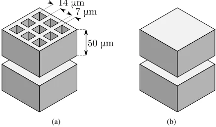
All floating structures need to have perforations for the release etch, this will be described in the fabrication process. Therefore, one of the normal structure plates is a grid of silicon beams as is illustrated in figure 11. This influences the capacitor model from equation 9, since the overlapping surface area decreases. These effects are simulated using FEM. The capacitance of a grid with the dimensions of figure 11 and a solid plate turned out to be approximately 11 % lower compared to the capacitance of two parallel plates. The fringing effects compensate for the holes in the plate.
7 μm 14 μm
50 μm
(a) (b)
Fig. 11. Parallel plate structure simulations. The capacitance of the situation with one perforated plate (a) performs 11 % lower compared to the situation with two solid parallel plates (b).
All parameters of the parallel plate structures are summa-rized in table IV.
TABLE IV
PARAMETERS OF THE PARALLEL PLATE STRUCTURES.
Quantity Symbol Value
Area of one plate Az 9.4·10−7m2
Perforation width and length Whole 14 µm
Grid beam width Wgrid 7 µm
Besides the parallel plate structures for measurements, there are several static parallel plate capacitor structures in the
sensor for reference measurements. These capacitors are not able to move and can be used to compensate for temperature and humidity effects.
F. Prevention of stiction
To achieve high sensitivity, large capacitor structures are needed. But care must be taken when designing such large floating structures, as stiction may occur. All large floating structures (figure 8 and figure 10) can be modeled as doubly clamped beams since they are always supported at two ends, this is illustrated in figure 12.
(a)
[image:5.612.379.494.207.340.2](b)
Fig. 12. Paths in the structures that can be modeled as doubly clamped
beams (a) or beams with a free end (b).
Following equation gives the maximum length for these structures [18].
Lcritical= 2.94
s
3 8
ET3 deviceg2
γs
≈3000µm, (17)
with Lcritical the critical length, E Young’s modulus (of
silicon), T the thickness of the beams (i.e. the thickness (50 µm) of the device layer), g the gap between the device layer and the handle layer (4 µm) andγs the adhesion energy
(assumed to be 100 mJ m−2). As a result of above equation,
all doubly clamped structures are less than 3000 µm in length. For structures with a free end, Lcritical should be 2.9 times
lower, hence, all structures that have a free end are always shorter than 1000 µm.
III. FABRICATION
A 100 mm p-type SOI wafer with a handle layer of 400 µm, a device layer of 50 µm and a box layer of 4 µm is used for the device.
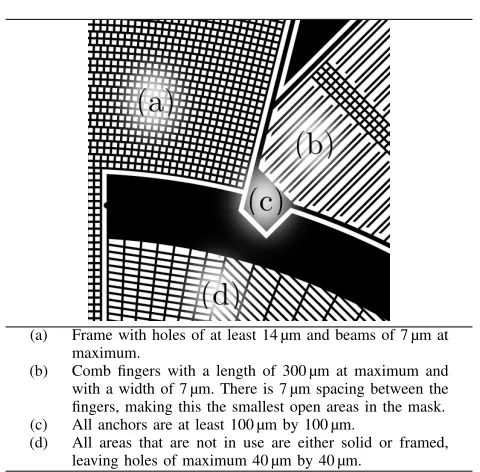
The fabrication process needs two masks: the mask for etching the handle layer and the mask for etching the device layer. The mask for the handle layer has relatively large structures. The rule of thumb of 1:10 [19] for aspect ratio is maintained, giving a minimum size for the trenches of 40 µm. The trenches are chosen slightly larger with 50 µm.
[image:5.612.58.276.436.564.2]The device layer contains more complicated structures. Table V gives the design rules that are related to the embedded figure with a closeup of the most complicated structures.
[image:5.612.72.274.669.710.2]TABLE V
DESIGN RULES WITH A CLOSEUP OF THE DEVICE LAYER.
(a) Frame with holes of at least 14 µm and beams of 7 µm at
maximum.
(b) Comb fingers with a length of 300 µm at maximum and
with a width of 7 µm. There is 7 µm spacing between the fingers, making this the smallest open areas in the mask.
(c) All anchors are at least 100 µm by 100 µm.
(d) All areas that are not in use are either solid or framed,
leaving holes of maximum 40 µm by 40 µm.
[image:6.612.55.295.70.306.2]There is a trench around the chip in both the handle layer and the device layer. There are small mounting points on both sides of the chip to fix the chips in the wafer. Releasing of the samples can be simply done by breaking them out. This technique does not need a dicing machine or other advanced methods and it allows arbitrary shapes for the chips. The trenches around the chips are the same as the smallest trenches on the chip (i.e. 7 µm for the device layer and 50 µm for the handle layer) to prevent damage to the oxide layer and possible leakage while etching.
Fig. 13. Impression of the location of the chips and how they can be broken
out of the wafer.
A. Wet oxidation and lithography
Wet oxidation (figure 14(b)) was done at 1150◦C. After 14 hours, the wafers had an oxide layer of 1963 nm. The SOI wafers were coated with positive photoresist (Fujifilm OiR 907-17).
B. Oxide etching and resist stripping
Etching of oxide was done using reactive ion etching (RIE) with an Adixen AMS100. A standard Bosch process was
used with a recipe based on an argon (Ar) and fluoroform (CHF3) chemistry. Both sides of the wafer were etched for
6 min (figures 14(d) and 14(g)). Resist stripping was done in O2-plasma using a Tepla 300E and nitric acid (HNO3)
(figures 14(e) and 14(h)).
(a)
(b)
(c)
(d)
(e)
(f)
(g)
(h)
(i)
(j)
(k)
silicon silicon dioxide photoresist
[image:6.612.52.301.459.582.2](l)
Fig. 14. Fabrication process: (a) SOI wafer, (b) oxidation, (c) lithography
on handle layer, (d) etching of oxide on handle layer, (e) resist stripping, (f) lithography on device layer (g) etching of oxide on device layer, (h) resist stripping, (i) etching of handle layer, (j) etching of device layer, (k) release etch, (l) materials.
C. Handle layer and device layer etching
The handle layer was etched using DRIE with an Adixen AMS100. Sulfur hexafluoride (SF6) was used as etchant and
flurocarbon (C4F8) was used for the deposition of passivation
layers. The handle layer etch underwent the process for 37 min (figure 14(i)). The device layer etch took 17 min (figure 14(j)). The fluorocarbon residues were removed using piranha clean-ing and O2-plasma.
D. Release etch
through the box layer of the SOI wafer. To prevent capillary forces making the structures snap to eachother, the final release etch was done using vapor HF and took 30 min (figure 14(k)).
Fig. 16. Photo of a fabricated force/torque sensor. The sensor has a diameter
of 9.24 mm and a thickness of 0.45 mm.
E. Fabrication results
The under etching was checked by removing several anchors of the device layer with a piece of tape. The anchors were between 5 µm and 10 µm under etched, which is enough to release the structures and not too much to release the anchors, since all floating structures are at maximum 10 µm by 10 µm and all anchors are at least 100 µm by 100 µm. By breaking the chip, potential tapering was inspected with scanning electron microscopy (SEM). But this appeared to be negligible. figure 15 contains SEM images of the result.
F. Final assembly
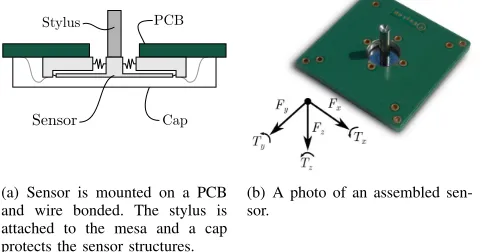
A hole is drilled in a printed circuit board (PCB). The sensor is mounted with the handle layer on the PCB using glue that cures when exposed to UV light. The sensor is wire bonded and a stylus is mounted using epoxy glue on the top of the suspended core through the hole in the PCB (figure 17).
Stylus PCB
Sensor Cap
(a) Sensor is mounted on a PCB and wire bonded. The stylus is attached to the mesa and a cap protects the sensor structures.
[image:7.612.112.238.103.208.2](b) A photo of an assembled sen-sor.
Fig. 17. Final assembly.
IV. CHARACTERIZATION
The force/torque sensor is characterized for five degrees of freedom, since there was no measurement setup realized for torques around normal axes (Tz).
(a) Overview of the device layer. (b) Close-up of the parallel plate structures.
(c) Close-up of the v-shaped springs. (d) Close-up of the comb-structures.
[image:7.612.319.560.167.293.2] [image:7.612.96.518.407.718.2]A. Method
The sensor’s force behavior is characterized by applying loads in shear and normal direction. An extra stylus is mounted on the back of the chip to make sure pure shear forces were applied. Torques around shear axes were measured by applying a load on the stylus at a defined distance from the sensor. The mechanical measurement setups for the three measurements are shown in figure 18.
x y
z
x y z
x y
z
m m
x y
z
m
(a)
[image:8.612.49.298.162.387.2](b) (c) (d)
Fig. 18. Measurement setups for applying loads to the sensor: (a) clamped
assembled sensor, (b) measuring normal force, (c) measuring shear force and (d) measuring torque.
The measurement electronics are schematically drawn in figure 19.
sensor
oscillators charge amplifier lock-in amplifier
V uout
Cfb
Crest+ΔC
uin
[image:8.612.329.555.386.508.2]Crest−ΔC
Fig. 19. Electronic setup for differential measurements including two oscilla-tors, a charge amplifier and a lock-in amplifier. Non-differential measurements are done using only one oscillator.
Measuring the (differential) change in capacitance is done using a custom built charge amplifier with a capacitor of 10 pF in the feedback loop. This makes the output of the charge amplifier as follows.
uout= 2∆C
Cf b
uin (18)
With uout the output voltage of the charge amplifier, uin
the input voltage, ∆C the differential change in capacitance and Cf b the feedback capacitance of the charge amplifier.
Two function generators (Agilent 33220A) with sine waves of 50 kHz with 180◦
phase shift are used for the input signals. The output of the charge amplifier is connected to a lock-in amplifier (Stanford Research Systems SR830) which was directly synchronized with one of the function generators.
B. Results
Figure 20 shows the results for applied shear forces, normal forces and torques. Shear force measurements (figure 20(a)) show a very linear (>99 %) differential change in capacitance with a sensitivity of 38 fF N−1. The values are corrected for
offset. The linear model is corrected for positive and negative shear forces with a factor of0.88 and0.78respectively.
-1e-13 -5e-14 0 5e-14 1e-13
-2.5 -2 -1.5 -1 -0.5 0 0.5 1 1.5 2 2.5
Normalized
dif
ferential
capacitance
[F]
Force [N] Model fit Meas.: X, load: X Meas.: X, load: Y
(a) Differential capacitance measurements of the comb-structures with varying shear forces.
-1.2e-12 -1e-12 -8e-13 -6e-13 -4e-13 -2e-13 0
0 0.5 1 1.5 2 2.5
Normalized
capacitance
[F]
Force [N] Model fit Meas.: Z, load: Z
(b) Capacitance measurements of the parallel plate structures with varying normal forces.
-2e-12 -1.5e-12 -1e-12 -5e-13 0 5e-13 1e-12 1.5e-12 2e-12
-0.006 -0.004 -0.002 0 0.002 0.004 0.006
Normalized
dif
ferential
capacitance
[F]
Torque [Nm] Model fit Meas: X, Torque: X Meas: X, Torque: Y
[image:8.612.50.301.467.580.2](c) Differential capacitance measurements of the parallel plate capacitors with varying torque.
Fig. 20. Measurement results.
[image:8.612.328.558.543.673.2]corrected for offset. A corrected model using the fourth order Maclaurin expansion from the design section is fit trough the measured values. The model is corrected for the distance between the parallel plates, the overlapping area of the plates and the stiffness with factors0.45,0.46and0.45respectively. The mentioned correction factors are necessary for the com-pensation of non-ideal effects in the mechanics, electrostatics or fabrication process. The distance between the capacitor structures may be smaller or larger than expected due to the etching process for example.
In figure 20(c) torque measurements around a shear axis are shown. The fitted model is based on a differential version of the normal force model.
The mounted styli on top and bottom of the sensor were the first parts that broke in the measurement setup. Mechanical robustness tests without styli show that the sensor can be safely overloaded in normal direction with more than 15 N without causing damage to the sensor.
V. DISCUSSION
The fabrication process and calibration will be discussed.
A. Fabrication
The mounting points that have to break for releasing the chips are too strong. This causes the need for a large force to remove the chips from the wafer. Besides, the very thin etched ring in the device layer (7 µm) caused the chips to get stuck after breaking the mounting points.
Some chips broke because of this and became instanta-neously useless, others were contaminated by particles and had to be cleaned in an ultrasonic bath. Most particles were removed in this way. Nevertheless, it is recommended to reduce the strength of the mounting points and increase the width of the etched rings around the chips.
B. Calibration
A slight crosstalk is observed when a shear force in orthogo-nal direction with respect to the measured direction is applied, caused by misalignment in the measurement setup (figure 20(a)). For this crosstalk is expected to be a consequent of the measurement setup, it is not included in the calibration matrix
K. The error bars in figure 20(a) represent misalignments from
−5◦ until 5◦.
Actual crosstalk occurs in the comb-structures when a torque is applied around shear axes. The rotation of the suspended core leads to a translation of the comb-structures as is illustrated in figure 21.
The crosstalk component is measured and its results are plotted in figure 22.
It can be concluded that the crosstalk measurements for forces applied at a distance of 1 cm of the sensor is in the same order of magnitude as for shear forces. However, there can be compensated for the crosstalk component using torque measurements with the parallal plate structures. Calibration matrix K is a six by eight matrix consisting of the inverted
↓Cx,−
[image:9.612.331.545.405.465.2]↑Cx,+ Tx
Fig. 21. Crosstalk in the comb-structures as consequence of an applied torque around a shear axis.
-1.5e-13 -1e-13 -5e-14 0 5e-14 1e-13 1.5e-13
-0.01 -0.006 -0.002 0.002 0.006 0.01
Normalized
dif
ferential
capacitance
[F]
Torque [Nm]
Fig. 22. Differential capacitance measurements of the comb-structures with
varying torques.
elementsβ−1and mentioned crosstalk componentsα−1.
Cali-bration matrixKis only valid for small forces and torques in the linear region. Expressions for the elementsβ−1
x andβ −1 z
were already given in equations 13 and 11.
K=
β−1
x βx−1 0 0 −α−x1 α−x1 −α−x1 α−x1 0 0 β−1
y β−y1−α−y1 αy−1 −α−y1 α−y1 0 0 0 0 β−1
z βz−1 βz−1 βz−1 0 0 0 0 β−1
φ β
−1
φ −β
−1
φ −β
−1
φ 0 0 0 0 β−1
θ −β
−1
θ β
−1
θ −β
−1
θ N/A N/A N/A N/A N/A N/A N/A N/A
(19)
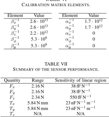
Characterization has been done and the crosstalk compo-nents are defined. The elements of calibration matrixKcan be calculated from the measurement results and are enumerated in figure VI.
TABLE VI
CALIBRATION MATRIX ELEMENTS.
Element Value Element Value
β−1
x 2.6·1013 α−
1
x 1.7·1012
β−1
y 2.6·1013 α−
1
y 1.7·1012
β−1
z 2.2·1012 α−
1
z 0
β−1
φ 5.3·109 α−
1
φ 0
β−1
θ 5.3·109 α−
1
θ 0
TABLE VII
SUMMARY OF THE SENSOR PERFORMANCE.
Quantity Range Sensitivity of linear region
Fx 2.16 N 38 fF N−1
Fy 2.16 N 38 fF N−1
Fz 2.34 N 550 fF N−1
Tx 5.84 N mm 23 nF N−1m−1
Ty 5.84 N mm 23 nF N−1m−1
[image:9.612.342.528.535.735.2]VI. CONCLUSION
A miniature large range five degrees of freedom force/-torque sensor is designed, realized and characterized. The first measurements were presented. It has a minimum force range of 2 N in shear and normal direction and a torque range of more than 6 N mm. The sensor shows in shear and normal direction competing sensitivities of 38 fF N−1 and 550 fF N−1
respectively. The proposed sensor is therefore suitable for biomechanical and robotic applications. The fabrication takes only two masks, making it a cheap and relatively fast process. The fabrication is also expected to be very reproducable, making it an interesting process for mass production. The rotation around the normal axis can be measured by the sensor, but is not yet characterized. Future work will focus on further characterization of this sixth degree of freedom, mechanical compensation for the crosstalk component and increasing the range and sensitivity.
REFERENCES
[1] A. F. Mak, M. Zhang, and D. A. Boone, “State-of-the-art research
in lower-limb prosthetic biomechanics-socket interface,” Journal of
rehabilitation research and development, vol. 38, no. 2, pp. 161–173, 2001.
[2] M. W. Legro, G. Reiber, M. del Aguila, M. J. Ajax, D. A. Boone, J. A. Larsen, D. G. Smith, and B. Sangeorzan, “Issues of importance reported
by persons with lower limb amputations and prostheses,”Journal of
rehabilitation research and development, vol. 36, no. 3, 1999. [3] P. H. Veltink, H. Kortier, and H. M. Schepers, “Sensing power transfer
between the human body and the environment,”Biomedical Engineering,
IEEE Transactions on, vol. 56, no. 6, pp. 1711–1718, 2009.
[4] K. Hirai, M. Hirose, Y. Haikawa, and T. Takenaka, “The development of
honda humanoid robot,” inRobotics and Automation, 1998. Proceedings.
1998 IEEE International Conference on, vol. 2. IEEE, 1998, pp. 1321– 1326.
[5] J. Butterfaß, M. Grebenstein, H. Liu, and G. Hirzinger, “Dlr-hand ii:
Next generation of a dextrous robot hand,” inRobotics and Automation,
2001. Proceedings 2001 ICRA. IEEE International Conference on,
vol. 1. IEEE, 2001, pp. 109–114.
[6] J. A. Dobrzynska and M. A. M. Gijs, “Capacitive flexible force sensor,” Procedia Engineering, vol. 5, pp. 404–407, 2010.
[7] E. S. Hwang, J. Seo, and Y. J. Kim, “A polymer-based flexible tactile sensor for both normal and shear load detections and its application for
robotics,”Journal of Microelectromechanical Systems, vol. 16, no. 3,
pp. 556–563, 2007.
[8] L. Beccai, S. Roccella, A. Arena, F. Valvo, P. Valdastri, A. Menciassi, M. C. Carrozza, and P. Dario, “Design and fabrication of a hybrid silicon
three-axial force sensor for biomechanical applications,”Sensors and
Actuators A: Physical, vol. 120, no. 2, pp. 370–382, 2005.
[9] H. K. Chu, J. K. Mills, and W. L. Cleghorn, “Design of a high sensitivity
capacitive force sensor,” in7th IEEE Conference on Nanotechnology.
IEEE, 2007, pp. 29–33.
[10] H. Muhammad, C. Oddo, L. Beccai, C. Recchiuto, C. Anthony, M. Adams, M. Carrozza, D. Hukins, and M. Ward, “Development of a bioinspired MEMS based capacitive tactile sensor for a robotic finger,” Sensors and Actuators A: Physical, vol. 165, no. 2, pp. 221–229, 2011. [11] H. K. Lee, J. Chung, S. I. Chang, and E. Yoon, “Normal and shear force measurement using a flexible polymer tactile sensor with
embed-ded multiple capacitors,”Journal of Microelectromechanical Systems,
vol. 17, no. 4, pp. 934–942, 2008.
[12] Y. Takei, K. Noda, T. Kawai, T. Tachimura, Y. Toyama, T. Ohmori, K. Matsumoto, and I. Shimoyama, “Triaxial force sensor for lingual
motion sensing,” in IEEE 25th International Conference on Micro
Electro Mechanical Systems (MEMS). IEEE, 2012, pp. 128–131. [13] R. Brookhuis, T. Lammerink, R. Wiegerink, M. de Boer, and M.
El-wenspoek, “3d force sensor for biomechanical applications,” Sensors
and Actuators A: Physical, vol. 182, pp. 28–33, 2012.
[14] R. Puers, “Capacitive sensors: when and how to use them,”Sensors and
Actuators A: Physical, vol. 37, pp. 93–105, 1993.
[15] H. Soemers,Design principles for precision mechanisms, 2010.
[16] E. Oberg, F. D. Jones, H. L. Horton, and H. H. Ryffel,Machinery’s
Handbook, 27th ed. Industrial Press, 2004.
[17] R. P. Feynman, R. B. Leighton, and M. Sands,The Feynman lectures on
physics, vol. 2: Mainly electromagnetism and matter. Addison-Wesley, 1979.
[18] N. Tas, T. Sonnenberg, H. Jansen, R. Legtenberg, and M. Elwenspoek,
“Stiction in surface micromachining,”Journal of Micromechanics and
Microengineering, vol. 6, no. 4, p. 385, 1996.
[19] H. Jansen, M. De Boer, S. Unnikrishnan, M. Louwerse, and M. Elwen-spoek, “Black silicon method X: a review on high speed and selective plasma etching of silicon with profile control: an in-depth comparison between Bosch and cryostat DRIE processes as a roadmap to next
gen-eration equipment,”Journal of micromechanics and microengineering,