S
u r f a c e
This document may not be copied, in whole or in part, without the prior written consent of Meiko World Incor-porated.
© copyright 1995 Meiko World Incorporated.
The specifications listed in this document are subject to change without notice.
Meiko, CS-2, Computing Surface, and CSTools are trademarks of Meiko Limited. Sun, Sun and a numeric suffix, Solaris, SunOS, AnswerBook, NFS, XView, and OpenWindows are trademarks of Sun Microsystems, Inc. All SPARC trademarks are trademarks or registered trademarks of SPARC International, Inc. Unix, Unix System V, and OpenLook are registered trademarks of Unix System Laboratories, Inc. The X Windows System is a trade-mark of the Massachusetts Institute of Technology. AVS is a tradetrade-mark of Advanced Visual Systems Inc. Verilog is a registered trademark of Cadence Design Systems, Inc. All other trademarks are acknowledged.
Circulation Control:
Meiko’s address in the US is: Meiko
130 Baker Avenue Concord MA01742 508 371 0088 Fax: 508 371 7516
Meiko’s address in the UK is: Meiko Limited
650 Aztec West Bristol
BS12 4SD
Tel: 01454 616171 Fax: 01454 618188
2.
MK403 Board Description . . . .
3
MBus. . . 5
ROSS Pinnacle Module . . . 6
Texas Instruments Viking Module . . . 7
Vector Processing Elements . . . 8
Memory Management. . . 9
Cache Coherency . . . 9
Fujitsu MB92831 Micro Vector Processor . . . 11
SBus Interfaces . . . 12
Memory Configuration . . . 12
IO Bus . . . 13
Board Control Processor . . . 14
3.
Using the MK403. . . .
15
Installation . . . 15
Removing the Module’s Front Panel . . . 15
Installing the Processor Board . . . 16
Boot ROM and H8 ROM . . . 20
Realtime Clock and Battery backed RAM . . . 20
Fuses. . . 20
External Connections . . . 20
Front Panel Connections. . . 21
RS232 Connections . . . 21
External Indicators . . . 22
A.
Address Maps . . . .
23
MBus Address Maps . . . 23
MBus Address Map Summary . . . 24
DRAM and SBus Slots . . . 26
µVP Cache Directory Mappings. . . 27
µVP Status and MMU Mappings . . . 28
BootRom, Serial Ports, Miscellaneous . . . 29
Control Area Network Interface . . . 30
Interrupt Request Control and Status Registers . . 31
STDIO IO Bus Control Registers . . . 33
MBus to SBus, Elan, and MBus Slot Slaves. . . 33
Vector Processors . . . 35
uVP Address Map . . . 36
B.
NVRAM Variables . . . .
39
C.
Forth Monitor Commands . . . .
45
CAN Commands . . . 45
Testing the CAN Device. . . 46
CAN Addresses . . . 49
Querying CAN Objects . . . 50
The MK403 Vector Processing Element offers high performance vector comput-ing power and flexible I/O options.
The board design encompasses at the lowest level the principle design objectives for the CS-2, offering a scalable modular construction with easy upgrade options, a reliance on state of the art commodity components, leading edge proprietary network components, and support for system wide fault tolerance.
In outline the Vector Processing Element offers:
•
Superscalar SPARC MBus module for scalar computing power and operating system services.•
Meiko Elan Communications Processor offering a high bandwidth, low latency interface to the CS-2 data network.•
Two Fujitsu Vector Processing Units (VPUs) on a plug-in module.•
Up to 128Mbytes of memory with 3 independent ports allowing simultaneous access by the SPARC MBus and the 2 Vector units.•
Three full size SBus slots for SCSI, Ethernet, or other third party options.•
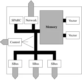
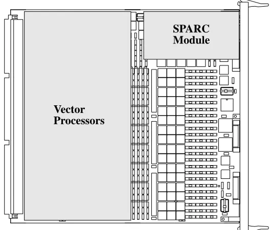
Keyboard, mouse, and dual serial ports.Figure 1-1 MK403 Board Overview
SBus SPARC
SBus SBus
Control
Network
Memory
Vector
Access by the 3 processors to the memory system is via three independent mem-ory ports. One port of the memmem-ory system is connected to an industry standard MBus interface giving access to the SPARC processor, the Elan Communications Processors, the MBus to SBus interface and its 3 SBus slots, and various other minor I/O devices on an I/O bus; in essence a SPARC workstation. Each of the remaining memory ports are used by the Fujitsu micro vector processors.
The 2 vector processing units on the MK403 are mounted on a single plug-in board which offers memory management and cache coherency with the SPARC caches. Cache coherency between the SPARC and vector processors has been achieved by defining a cache directory close to each vector processor; this cache directory attempts to replicate the contents of the SPARC cache tags/state, and is therefore potentially updated on every MBus cycle. Memory accesses by the vec-tor processors that conflict with the SPARC cache cause the vecvec-tor processor to stall until the appropriate MBus cycles have been generated.
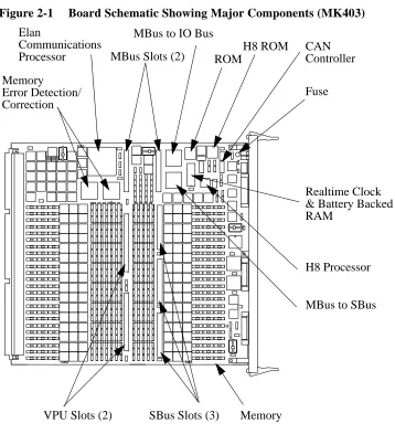
The major components and their placement on the MK403 motherboard are shown in Figure 2-1.
Figure 2-1 Board Schematic Showing Major Components (MK403) Elan
Communications
Processor MBus Slots (2)
SBus Slots (3) VPU Slots (2)
H8 ROM ROM
MBus to IO Bus
H8 Processor Realtime Clock & Battery Backed
MBus to SBus Fuse
Memory
CAN Controller
MBus, SBus, and Vector Processor plug-in modules not shown. Components are also fitted on the reverse of this board.
Memory
Error Detection/ Correction
Figure 2-2 Board Schematic Showing Major Components (MK534)
MBus
Two full size MBus sites are provided. One of these is used by the plug-in vector processors, the other by a uni-processor SPARC MBus module.
The MBus is fully level 2 compliant and runs at 40MHz. The SPARC processor shares the MBus with the Elan Communications Processor, the MBus-to-SBus interface, the I/O bus controller, and vector processors (but note that the vector board uses the MBus interface solely for memory management and cache coher-ency with the SPARC, and that direct memory accesses are made via memory ports that are independent of the MBus). The allocation of MBus id’s is:
•
MBus id 0 is the I/O bus controller.•
MBus id 4 is the MBus to SBus controller.•
MBus id 6 is the Elan Communications Processor.•
MBus id’s 8 and 9 are MBus slot 0.•
MBus id’s 10 and 11 are MBus slot 1. VectorMBus slot 0 is always used by the plug-in vector board. MBus slot 1 is always used by a uni-processor SPARC module, currently either a TI Viking (with or without second level cache) or a ROSS Pinnacle.
ROSS Pinnacle Module
The MK403 may be fitted with a uni-processor Pinnacle module which includes second level cache.
The Pinnacle MBus module is built upon a tightly coupled set of three ROSS de-vices: the RT620 HyperSPARC CPU, the RT625 cache controller, memory man-agement, and tagging unit (CMTU), and the RT627 cache data units (CDUs).
Features of the RT620 CPU are:
•
SPARC version 8 conformance.•
90MHz clock rate.•
4 execution units offering parallel execution of major instruction types: Load/Store, Branch/Call, integer and floating point units.•
Dual instruction fetch per clock cycle.•
8Kbyte 2-way set-associative on-chip instruction cache.•
Instruction pipelining including a cache stage to accommodate the latency for second level cache accesses on data. Simultaneous accesses to on-chip and second level cache for each instruction fetch.•
High bandwidth 64bit Intra Module Bus (IMB) provides the interface between the CPU and the second level cache. Use of second level cache decouples the processor clock rate from the lower MBus clock rate.Key features of the RT625 (CMTU) and RT627 (CDU) devices are:
•
Full level 2 cache-coherent MBus compatibility.This chapter describes the usage of the MK403 in terms of its installation, hard-ware interfaces, and field serviceable components.
Installation
The MK403 is designed for use solely in a CS-2 Processor Module. The Proces-sor Module supplies the board’s power, cooling, and connection to the CS-2 data and control networks. The MK403 is fitted into one of the four vertical board slots behind the Processor Module’s removable front panel.
Warning – You must disconnect the power fr om the Processor Module be-fore removing or installing pr ocessor boards.
Warning – The board may be fitted with fragile or static sensitive devices. You must handle with car e and observe anti-static pr ecautions.
Removing the Module’s Front Panel
The module’s front panel is held in position by four clips, one in each corner. To remove the panel pull firmly away from the module.
Use the reverse procedure to install the LEDs and front panel.
Installing the Processor Board
Insert the board so that it fits into the guide rails at the top and bottom of the mod-ule’s board rack, ensuring that the component side is to the left (viewed facing the module). Gently push the board squarely on its front panel. Before pushing the board fully into position fold back the levers at each end of the front panel so that they are at 90o to the board; now push the board (while holding the levers) until the base of the two levers is touching the card cage. To lever the board into its final position push both levers until they lie flat on the board’s front panel. Se-cure the board by tightening the two captive screws.
Use the reverse procedure to remove the board.
Warning – You should take car e not to damage the connectors at the r ear of the board and on the module’ s backplane. Ensur e that the board mates squarely with the module’ s backplane.
Warning – When r emoving or installing a board you should take car e not to damage the RFI (copper) seals along the edge of the board’ s front panel.
Warning – To maintain pr oper circulation of cooling air and to conform to RFI regulations all board slots must be fitted with a pr ocessor board or blanking plate.
Field Serviceable Components
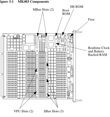
The MK403 has the following field upgradeable components (see Figure 3-1):
•
Superscalar SPARC processor module fitted to MBus slot.•
Three SBus slots.•
Two vector processor slots.•
H8 ROM.•
Realtime clock and non-volatile RAM module.•
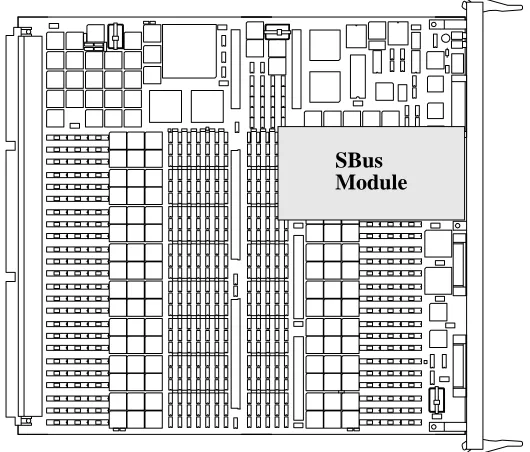
Fuses.Figure 3-1 MK403 Components MBus Slots (2)
SBus Slots (3) VPU Slots (2)
H8 ROM Boot
Realtime Clock and Battery Fuse ROM
Processor Modules
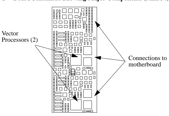
The 2 vector processor are mounted on a single plug-in board (MK534) which is connected to MBus slot 0 and both of the VPU slots. The board is fixed in place by 4 M3 screws.
A single uni-processor SPARC module is connected to MBus slot 1. The MK403 motherboard includes support for either Texas Instruments Viking or ROSS Pin-nacle module (although PinPin-nacle modules are typically used). The type of SPARC module is set when the MK403 board is manufactured and may not be reconfigured on site.
Figure 3-2 Position of the Vector and SPARC Modules
SPARC Module
Installing SBus Modules
Three SBus slots are provided and these may be fitted with standard SBus mod-ules; these are plugged into the SBus connectors and secured with two M3 screws. When using SBus cards that have external connections, for example a graphics card, remove the appropriate panel from the front of the MK403 — the panel is held in place by two small screws.
SBus devices are numbered from 0 to 2, device 0 being next to the processor slots (see Figure 3-3).
Figure 3-3 Position of SBus Module 0
SBus SCSI Cards
When using SBus SCSI cards to connect to disk devices within the Processor Module you must connect the front-panel output from the SBus card to the SCSI-A connector on the MK403 motherboard using Meiko cable 60-CSCSI-A0217-1T.
You should note that the Processor Module’s disks may be interconnected in one of three ways: each of the 4 disks connected to a separate processor board via SCSI bus A, disks connected in pairs to SCSI bus A on board’s 0 and 1, or all disks connected to SCSI bus A on board 0.
Boot ROM and H8 ROM
Both of these ROMs may be upgraded from time to time. They are held in sockets and are readily replaced. Note the position on pin 1 before removing the old de-vice (usually marked by a dot on the packaging).
Realtime Clock and Battery backed RAM
The real time clock and non-volatile RAM device is held in a DIL socket and is easily replaced. Before removing the old device note the position of pin 1 (usu-ally marked by a dot on the packaging). Note that the information within the RAM can only be restored by Meiko’s engineers.
Warning – This device contains lithium batteries; never dispose of this de-vice in a fir e or attempt to dismantle.
Fuses
There is one fuse on the MK403 motherboard to protect the keyboard/mouse cir-cuit. This is a 250mA quick blow fuse, Meiko part number 22-FU400-02E250.
External Connections
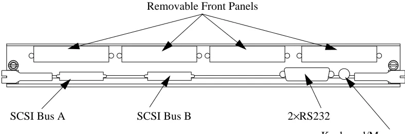
Front Panel Connections
Removable panels provide access to connectors on the optional SBus boards.
Figure 3-4 MK403 Front Panel Connections
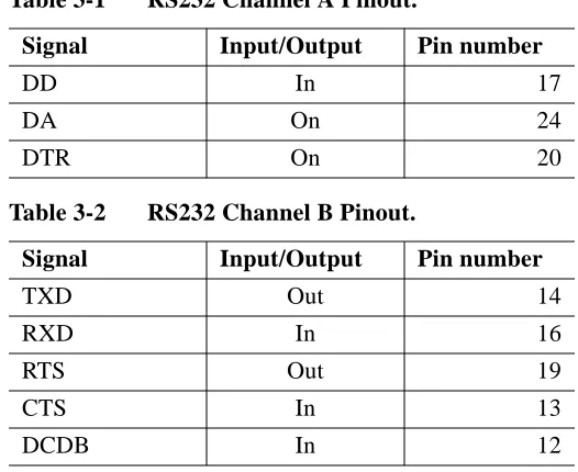
RS232 Connections
The two RS232 channels are output via a single 25-way connector. The connec-tions are as shown in the following tables. Signal ground is pin 7, chassis ground in pin 1.
Table 3-1 RS232 Channel A Pinout.
Signal Input/Output Pin number
TXD Out 2
RXD In 3
RTS Out 4
CTS In 5
CSR In 6
DCD In 8
DB In 15
Removable Front Panels
SCSI Bus A SCSI Bus B 2×RS232
External Indicators
Two LEDs (one green, one amber) are included on the board’s front panel. The green LED is the heart beat from the board’s (H8) CAN controller. The amber light illuminates each time the CAN controller transmits on the CAN bus. Both should flash steadily. These indicators are also displayed on the module’s LED display.
The green LED flashes at a slow steady rate (once per second) when operating normally. A quicker flash rate (2×normal) indicates that the board’s SPARC processor is not responding; a very quick flash rate (3×normal) indicates that the H8 processor on the module’s controller is not responding.
Each processor board within a processor module controls a 4×4 matrix of red LEDs on the module’s front panel. The MK403 displays a random pattern on these when running the Boot ROM. When Solaris has been booted a circulating pattern is displayed. The pattern can be changed by user programs and various system commands and daemons.
DD In 17
DA On 24
DTR On 20
Table 3-2 RS232 Channel B Pinout.
Signal Input/Output Pin number
TXD Out 14
RXD In 16
RTS Out 19
CTS In 13
DCDB In 12
Table 3-1 RS232 Channel A Pinout.
MBus Address Maps
This section gives the mapping of memory and peripherals into the MBus phys-ical address space. All addresses are in hexadecimal, all locations are word wide unless otherwise stated in the notes. The following notes are associated with some of the items in the tables:
1. These locations are byte wide and are mapped into all 4 bytes of a word. Care should be taken to generate correct bytewide accesses to the least significant byte of the word in order to maintain future compatibility.
2. These locations are halfword wide and are mapped into both halfwords of the word. Care should be taken to generate correct halfword accesses to the least significant halfword of the word in order to maintain future compatibility.
3. These locations are bytewide memory, mapped into contiguous byte locations. Word or halfword accesses will be automatically mapped into several succes-sive bytewide accesses.
µ
VP Status and MMU Mappings
a. The MMU RAM mappings should be such that Logical Address equals Physical Address, or the MMU RAMS should be accessed by bypassing the SPARC MMU. This allows the addresses to behave the same, regardless of whether we are con-figured as a Pinnacle or a Viking.
MBus Address Usage Rd/Wr Note
900000000 to 90001fff8a
µVP MMU (write both, readµVP 0) RW
910000000 to 91001fff8
µVP MMU (read-only ofµVP 1) R
920000000 MMU_ADDRESS0 R
920000000 LD_PF_INBOUND (note same address as above!)
W
930000000 MMU_ADRESS1 R
930000000 LD_PF_OUTBOUND (note same address as above!)
W
980000000 MMU_CONTROL W
980000008 MMU_MASK_FAULT W
980000010 MMU_CLEAR W
980000018 KILL_uVP W
980000028 CLEAR_INVALIDATE W
9A0000000 uVP Status R
9A0000010 SET_GATE_AND_SYNCH W
80000000 µVP EDC Error Data
80000008 µVP EDC Error Diagnosis
The battery-backed RAM in the realtime clock module is used to used to store basic machine start-up and communication options.
These parameters may be queried using the Forth Monitor (i.e. at theok prompt):
For example:
Alternatively the System Administrator can use theeeprom(1m) command to view and change the variables direct from a Unix command shell. For example:
Some of the parameters (those marked in the following list) may also be modified using the Set function in Pandora’s Network and Configuration Views.
printenv Display current variable settings.
setenv variable value Assign (or reassign) a value to a variable.
set-default variable Restore the variables default value.
set-defaults Restore the default values to all variables.
ok setenv output-device can
Variable Default Description
sbus-probe-list 43012 Identifies the SBus slots to probe and the probe order.
keyboard-click? false If true, enable keyboard click.
keymap no default Name of custom keymap file.
output-device
†
screen Power-on output device. One ofscreen,can,ttya, orttyb. Usecan to enable console connections to be grabbed bycancon(1m) and Pandora.
input-device
†
keyboard Power-on input device. One ofkeyboard,can,ttya, orttyb. Usecan to enable console connections to be grabbed bycancon(1m) and Pandora.
cancon-host 4294967295 Used to record the host of thecancon(1m) remote console connection through a reboot of this
processor. Do not change.
elanip-broadcast-high
†
4096 Highest Elan Id in network.elanip-broadcast-low
†
0 Lowest Elan Id in network.ep-btxpktlifetime
†
1000 Elan packet characteristics.ep-btxtimeout
†
1000 Elan packet characteristics.ep-txpktlifetime
†
10000 Elan packet characteristics.ep-txtimeout
†
10000 Elan packet characteristics.ep-bigmsgbcastboxes
†
4 Elan packet characteristics.ep-bigmsgboxes
†
32 Elan packet characteristics.ep-bigmsgsize
†
20416 Elan packet characteristics.ep-smallmsgbcastboxes
†
4 Elan packet characteristics.ep-smallmsgboxes
†
32 Elan packet characteristics.ep-smallmsgsize
†
4032 Elan packet characteristics.The following commands have been added to the Forth Monitor and are in tion to the commands that are normally present on a Solaris system. The addi-tional commands relate to the Control Network (CAN) and Elan network.
CAN Commands
To test and use the CAN bus you need to understand CAN addresses.
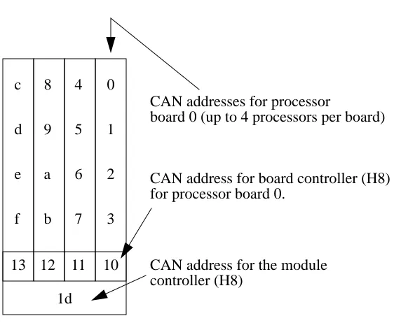
Nodes are addressed by their physical position in terms of Cluster, Module, and Node id’s (CMN). In CAN packets each of these id’s is represented by a 6bit field; the hexadecimal representation of these three 6bit fields is a Node Id.
The module id is derived from the switch at the rear of the module. The number-ing of the nodes within a module is shown in Figure C-1.
Testing the CAN Interface Device
Thetest command tests the SPARC’s CAN device by writing various values into its test register. The test is repeated using the test registers on the board con-troller’s H8 and the module concon-troller’s H8.
Testing the CAN Bus
You can test the CAN bus connection between nodes by using thertest com-mand. In the following example data is transferred from the current node to node 4:
ok test /can
Register test 0x00: OK Register test 0xff: OK Register test 0xaa: OK Register test 0x55: OK Checking on-board H8: OK.
Checking module controller: OK.
ok 4 rtest
Performing remote write/read test on node 4 Remote node type is MK405
Checking the Board and Module Controllers
You can check that both the board controller and module controller H8 proces-sors are running by using theping-h8 andping-module commands. Note that you need to change directory to/can before you use these commands.
Querying CAN Bus Usage
You can query the utilisation of the CAN bus by using theperf command. This command shows the number of CAN packets received since the machine was powered-up, and the number since the last query. You need to change to the
/can directory before using this command:
ok cd /can ok ping-h8
On-Board H8 is MK401. ok cd ..
ok cd /can ok ping-module
Module controller is MK515. ok cd ..
ok cd /can ok perf
Monitoring CAN Bus Packets
You can snoop the CAN bus (monitor that packets on the bus) using thesnoop
command. Note that you cannot use this facility if you are connected to the Forth Monitor via a cancon connection. You need to change to thecan directory before using this command.
CAN Addresses
To determine the CAN address of this node use.can-id. This displays the node’s address in terms of its CMN, Node Id, and Slot Id. The Slot Id is for Meiko engineering use1.
Similarly the CAN address of the board’s controlling H8 processor can be ob-tained with the.h8-id command:
1. The slot id is the node’s physical position in the machine represented by a 5 bit cluster number, a 5 bit module number, a 2 bit slot number, 2 unused (always 0 bits), and a 2 bit processor number; the 2 bits that represent the slot number are transposed.
ok cd can ok snoop
Can’t can-snoop if you are a cancon slave ok cd ..
ok .can-id
SlotId: 0090, CAN Node-id: 00088 [00:02:08]
ok .h8-id
The CAN address of the H8 that controls the board’s module can be determined by the.module-id command:
You can convert from CAN node id’s to Cluster, Module, Node addresses (and vice versa) by using thecanid>cmn andcmn>canid commands respectively. Note that you need to change directory tocan before you use these commands.
Querying CAN Objects
Can packets include a 10 bit address space which, although not sufficient to map into the MBus/H8 physical address space, is adequate to map-in various status and control devices. These are referred to as CAN objects. Reading or writing to these objects allows you to query the status of a processor, board, or module, and to issue control instructions. See the header file /opt/MEIKOcs2/inclu-de/canio/canobj.h for a list of object addresses and their meanings.
Local CAN objects are those that relate directly to this node. Remote CAN ob-jects maybe those of a board, module controller, or remote SPARC.
ok .module-id
The module controller is node 0009d.
ok cd can ok 4 canid>cmn 0 0 4
ok cd ..
ok cd can
You use therlo command to read a local object. You need to pass an object id on the Forth stack; in the following example we request the board type and are returned 191 (an MK401):
To read a remote object you need to push onto the Forth stack a CAN node id and the object id. In the following example we request the board type of nodec1
(module 3, board 0, node 2), which is an MK405:
The following additional example fetches the board type of nodedd, which is the controller for module 3, cluster 0:
Similar commands exist to write to CAN objects, but their direct use is not rec-ommended (they can reconfigure and reset the machine).
Remote Console Connections
You can create a console connection to a remote node by usingcancon. You need to pass on the Forth stack a CAN node id.
ok 0 rlo Read: 191
ok c1 0 rro Read: 195
You cannot create acancon connection from within an existing cancon connec-tion. If you are remotely interacting with a node’s Forth monitor viacancon (or Pandora) an attempt to create anothercancon connection will fail.
If your node is currently serving a remote console connection to someone else you can force it to disconnect that connection by usingcancon-dis. In the fol-lowing example the current connection to node 8 is dropped:
Elan Commands
The Elan device includes self test code that can be executed by thetest-all
command (which tests memory, SBus, CAN, Elan and all other devices with self test code) or explicitly by thetest /elan command.
ok 4 cancon
Connected to node 00004
cs2-4 console login:
ok 8 cancon-dis
Disconnecting node 00008 [00:00:08] ...
ok test /elan
Initialising Elan/Selftest software ... OK Checking threads processor ... OK
Testing from level 1 to level 1. Generating a route to level 1 ... OK Ping ... OK
Check-Ping ... OK
Spraying data to top switch ... OK Testing spray buffer ... OK