Article
In-situ Mechanical Characterization of Mixed-Mode
Fracture Strength of Cu/Si Interface for TSV
Structures
Chenglin Wu *, Congjie Wei and Yanxiao Li
Department of Civil, Architectural, and Environmental Engineering, Missouri University of Science and Technology, Rolla, MO, USA
* Correspondence:[email protected]; Tel.: +1-573-341-4465
Abstract: In-situ nanoindentation experiment has been widely adopted to characterize material behaviors of microelectronic devices. This work introduces the latest developments of nanoindentation experiment in characterizing nonlinear material properties of 3D integrated microelectronic devices with through-silicon-vias (TSVs). The elastic, plastic, and interfacial fracture behavior of the copper via and matrix-via interface have been characterized using small scale specimens prepared with focused-ion-beam (FIB) and nanoindentation experiment. A brittle interfacial fracture was found at the Cu/Si interface under mixed-mode loading with a phase angle ranging from 16.7 to 83.7 degrees. The mixed-mode fracture strengths were extracted using the linear elastic fracture mechanics (LEFM) analysis and a fracture criterion was obtained by fitting the extracted data with the power-law function. The vectorial interfacial strength and toughness were found to be independent with mode-mix.
Keywords: TSV; nanoindentation; FIB; micro-cantilever beam; mixed-mode; fracture
1. Introduction
Thermal mechanical reliability plays a critical role in microelectronic devices affecting their performance and service life-spans. In-situ mechanical characterizations are essential to predict the thermal-mechanical behaviors of these devices. The associated techniques and approaches rapidly emerge along the technology growth in 3D integrated circuits and devices [1-7]. One of the typical approaches is the nanoindentation [6, 8, 9], which utilizes a small-scale probe with controlled force and displacement applied directly to the substrates or micro and nanostructures [10, 11]. Utilizing various sizes and shapes of the probe, the small-scale nonlinear material behavior can be characterized. This work focuses on the latest development of the nanoindentation techniques applied to 3D integrated microelectronic devices with through-silicon via (TSV).
As the microelectronic devices become smaller and more complex, 3D integration becomes necessary for more efficient engineering and design. This integration consists the micro-meter copper vias passing through silicon die serving as both electronical connections and mechanical supports. The copper vias were typically deposited by electroplating approach and have complex grain structures. Under such conditions, the TSVs share different material properties comparing to the bulk copper. Surface treatments were often conducted to the TSVs to avoid diffusion and enhance mechanical strength at Cu/Si interface. To have a comprehensive understanding of the mechanical behavior of TSV and related interface, in-situ small scale characterizations are required.
Nanoindentations have been widely adopted for in-situ characterization of mechanical properties of thin-films and nanostructured materials [6-11]. The elastic and plastic properties can be readily extracted using the force-displacement responses produced by nanoindentation with various tip shapes and sizes. In addition, miniature specimens prepared using focus-ion-beam (FIB) fabrication techniques can also be utilized to obtain more systematic understanding of the
deformation mechanisms at small-scales. Therefore, the combination of nanoindentation and FIB fabrication presents a unique opportunity in probing mechanical behavior of TSV structures and interfaces in 3D integrated microelectronic devices. In this paper, a cantilever beam approach for extracting mixed-mode interface strength is proposed. The nonlinear elastic-plastic behavior of the copper TSV is characterized using micro-pillar experiment. Miniature cantilever beams with various lengths were fabricated using FIB. Both analytical and numerical models were developed to extract the mixed-mode interfacial strength at the TSV/Si interface. The extracted results were then fitted with the power-law failure criterion [12-15] producing an input for failure prediction and reliability evaluations.
2. Materials and Sample Preparation
Figure 1. TSV specimens: (a) FIB-SEM dual beam system, (b) TSV in silicon substrate, schematics of (c) micro-pillar, (d) micro-cantilever experiments, SEM images of (e) micro-pillar adapted with permission from [8], (f) cantilever beam specimens.
Figure 2. Micro-cantilever beam specimens: (a) isometric view and structural components, (b) top view, and (c) side view with dimensional details (L = 4 µm).
3. Nanoindentation Experiment
The nanoindentation experiments were conducted using the Hysitron TI-95 Tribo-indenter® on both micro-pillar and micro-cantilever specimens with a flat-punch tip having diameters of 5 and 2 µm, respectively. The experimental details and subsequent extraction methods have been described in our previous work [8, 16]. For the micro-cantilever beam experiment, the flat punch tip was placed inside the loading crater of the loading pad to apply displacement-controlled loading. A loading rate of 0.5 nm/s was applied till the cantilever beam fails at the Cu/Si interface. It is worth noting here that the mechanical backlash was corrected during the tip-optic calibration process. A pre-loading with the maximum load of 1 µN was applied at the end of the beam to ensure a proper contact.
4. Analysis
4.1. Micro-pillar experiment
The force-displacement response obtained is shown in Figure 3a. Significant plastic responses were observed indicated by the permanent deformation after each unloading. The residual deformations were also confirmed by the SEM images shown in Figure 3a. To extract this observed elastic-plastic property, a finite element analysis was conducted considering the tapering caused non-uniform stress distribution [8, 16]. The Ramberg-Osgood power-law relationship [17] was adopted in the numerical models to compare with experimental results. In this relationship, the stress versus plastic strain response follows the description below,
𝜀
𝑝=
3 7𝜎𝑒
𝐸
(
𝜎𝑒𝜎0
)
𝑛−1
(1)
where 𝜀𝑝 is the plastic strain, 𝜎𝑒 is the equivalent stress, 𝜎0 is the yield stress (which is found to be
Figure 3. (a) Force-displacement response of micro-pillar experiment Reproduced with permission from [8], (b) stress-plastic strain relationship from Ramberg-Osgood relationship.
Figure 4. FEA analysis of micro-pillar experiment reproduced with permission from [8]
4.2. Micro-cantilever experiment
4.2.1. Failure surface characterization
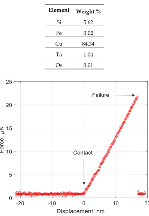
are shown in Table 1. As listed, most of the elements detected are Cu, which is followed by Si and elements in the liner materials at the TSV/Cu interface (Fe, Ta, Os). This result is similar to that of the shear failure surface from the previous work [8]. As previous concluded, the majority of the Cu signal comes from the background Cu materials in the TSV indicating an interfacial failure locus within the silicon matrix.
Table 1. Element and weight percentage of EDS.
Element Weight %
Si 5.62
Fe 0.02
Cu 84.34
Ta 1.04
Os 0.01
Figure 5. Typical force-displacement response of micro-cantilever beam (L = 4 µm).
Figure 7. (a) Illustration of micro-cantilever beam with pre-crack, (b) FEA mesh details (yellow indicates Cu, grey indicates Si), (c) normal stress at the crack tip, (d) shear stress at the crack tip.
4.2.2. Mixed-mode fracture
(1) LEFM analysis
The stress analysis for the micro-cantilever beam experiment was conducted using both LEFM and non-linear fracture mechanical model (NLEFM) considering the effect of Cu plasticity. Analytically, the far-field load generated near-field stress has both normal (𝜎0) and shear (𝜏0) components. From the Euler beam theory and ignore the nonlinear shear deformation caused by root rotation, these stresses can be obtained using the beam geometry and material constants of the silicon.
𝜎
0=
𝑃𝐿6𝑏ℎ2
,
𝜏
0=
3𝑃
2𝑏ℎ
(2)
The local stress at the crack tip can then be computed using these near-field stress and the stress intensity factor as
𝐾 = 𝐾
𝐼+ 𝑖𝐾
𝐼𝐼(3)
𝜎 =
𝑅𝑒(𝐾𝑎𝑖𝜖) √2𝜋𝑙,
𝜏 =
𝐼𝑚(𝐾𝑎𝑖𝜖)
√2𝜋𝑙
(4)
where 𝑎 is the crack length, 𝜖 = 1
2𝜋𝑙𝑛 ( 1−𝛽 1+𝛽), 𝛽 =
1 2
𝜇1(1−2𝑣2)−𝜇2(1−2𝑣1)
𝜇1(1−𝑣2)+𝜇2(1−𝑣1) are the materials mismatch parameters [18, 19], 𝜇𝑖, 𝑣𝑖 are shear modulus and Poisson’s ratio for Cu and Si respectively, where 𝑖 =
1, 2, 1 represents Cu, 2 represents Si. 𝑙 = 100 𝑛𝑚 which is the length scale for the investigated problem. The stress intensity factors are obtained using the LEFM FEA analysis.
The mesh details for the LEFM finite element analysis are shown in Figure 7a, where the plain strain 4-node bilinear quadrilateral elements were used in the region away from the crack tip. The singular elements were then used near the crack-tip with a square root singularity [20]. The normal, shear stress and strain contours of the analyzed micro-cantilever beam are shown in Figure 7b. The analysis was then conducted for the six types of specimens with given tested failure loads (𝑃) and geometrical characteristics. The phase-angle was defined in terms of stress [19] as 𝜓 =
arctan (𝐼𝑚(𝐾𝑎𝑖𝜖)
fracture strength corresponding with the associated phase angle. The vectorial fracture strength can also be obtained by Τ = √𝜎02+ 𝜏02. The fracture toughness was also calculated using the critical stress
intensity factors calculated following the equation [18] below,
Γ =
(1−𝛽2) 𝐸∗(𝐾
𝐼𝑐2
+ 𝐾
𝐼𝐼𝑐2
)
(5)
It should be noted here that these crack-tip stresses are essentially the stresses at 𝑙 away from the crack-tip. The effect of the plastic-zone was omitted since the calculate stresses at these distances are much smaller than the yield strength of the Cu (216 MPa). However, the NLEFM analysis was nevertheless conducted to justify the negligence of the plastic effect.
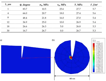
Table 2. Mixed-mode fracture analysis results.
L, µm 𝝍, degree 𝝈𝟎, MPa 𝝉𝟎, MPa 𝜯, MPa 𝜞, J/m2
1 83.7 10.5 25.6 27.7 5.7
4 66.0 20.7 18.0 27.4 5.6
8 48.4 21.8 16.0 27.0 5.4
12 36.9 25.0 10.0 26.9 5.4
18 26.6 26.3 5.0 26.8 5.3
30 16.7 26.7 0.0 26.7 5.3
Figure 8. NLEFM analysis results of micro-cantilever beam for L = 4 µm: (a) far-field view, (b) localized view near crack-tip showing equivalent plastic strain contour.
(2) NLEFM analysis
regime is labeled by the red-dashed circles. The radius of these circles range from 10 to 15 nm, which are smaller than the 100-nm characteristic length scale used in the LEFM analysis validating the obtained mixed-mode fracture results.
Figure 9. (a) phase angle versus beam length, (b) vectorial fracture strength and toughness versus phase angle,.
5. Results and Discussions
5.1. Size effect in Cu via
The yield strength measured from the micro-pillar experiment is close to those measured at the bulk scale. However, the hardening exponent (n = 3) measured at micro-scale is much less than those typically measured at bulk scale (n = 5) indicating a possible size effect caused by the reduced relative grain size. The average grain sizes measured for the TSV used in this study is about 500 nm [8], which is slightly smaller than the typical grain size observed at the bulk scale. The smaller grain size increases the total grain boundary area that contributing to the strain hardening mechanism as illustrated by Taylor’s theory [21-25]. This increased strain hardening behavior of Cu can effectively “lock” the plastic strain development within a small region as observed in shear fracture of our previous work as well as in the micro-cantilever beam experiment. Therefore, it is worth noting here that the Cu plasticity has limited effects on the interfacial fracture of Cu/Si interface. The NLEFM results also confirmed that the crack-tip induced stress singularity causes limited plastic effect, however was constrained within area that smaller than the characteristic length of the investigate interface.
5.2. Mixed-mode Cu/Si interfacial behavior
The phase angle versus the beam length (L) is plotted in Figure 9a. A decreasing trend was observed as the beam length increases. The range of the phase angle is from 16.7 to 83.7 degrees covering most part of the positive mode-mix (0-90 degrees) indicating a completeness of the experimental data set in determining the fracture criterion at the Cu/Si interface.
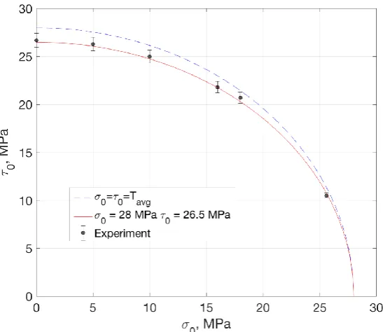
Given this results, a fracture criterion is then proposed for the tested Cu/Si interface. Following the power-law failure criterion proposed by Carlsson et al. [12], the failure strength of the Cu/Si interface can be descried as the following equation.
(
𝜎0𝜎𝑐
)
𝜆
+ (
𝜏0𝜏𝑐
)
𝜆
= 1
(6)
where 𝜎𝑐, 𝜏𝑐 are the fracture strength for pure mode-I (normal) and mode-II (shear). 𝜆 is a fitting
parameter which was set at 1.8. The measured experimental data are then fitted with the proposed failure criterion as shown in Figure 10. The dashed blue line shows the fitting of experimental data with 𝜎𝑐= 𝜏𝑐 = 𝑇𝑎𝑣𝑔. The red solid line shows the fitting of 𝜎𝑐 = 28 𝑀𝑃𝑎, 𝜏𝑐 = 26.5 𝑀𝑃𝑎. The better
fitting of the experimental was observed when setting different fracture strengths for pure mode-I and mode-II. This results indicates that the mode-mix still has moderate effect on the fracture strength although the vectorial value stays almost constant.
Figure 10. Failure criterion and experimental data.
6. Conclusions
This work combines the micro-pillar compression and micro-cantilever experiments to extract the mixed-mode fracture strength of the Cu/Si interface at small scale (<100 nm). A series of micro-cantilever beam specimens with various beam lengths were fabricated and tested covering almost full range of the positive mode-mix (0~90 degrees). Following conclusions are drawn from the experiment and analysis results:
(1) The mixed-mode fracture at the Cu/Si interface is brittle in nature. No significant cohesive zone was observed nor the plastic hinge that typically found for micro-cantilever beam consists of metal materials.
(2) The effect of the plastic behavior of the Cu is negligible. The NLEFM analysis results have shown that this is mostly due to the constrained plastic region, which is much smaller than the characteristic length (100 nm).
(3) The vectorial fracture strength and toughness were obtained from the analysis indicating the effect of mode-mix is limited, which is suspected to be related to the constrained plastic zone.
Future studies will focus on evaluation of effects of residual stress, interfacial defects, and impurities of Cu on the mixed-mode interfacial strengths.
Acknowledgments: The author would like to thank the seed funding from Material Research Center for this project.
Author Contributions: Chenglin Wu and Yanxiao Li conceived and designed the experiments; Chenglin Wu performed the experiments; Chenglin Wu and Congjie Wei analyzed the data; Chenglin Wu contributed reagents/materials/analysis tools; Chenglin Wu and Congjie Wei wrote the paper.
Conflicts of Interest: The authors declare no conflict of interest.
References
1. Garrou, P., C. Bower, and P. Ramm, Handbook of 3D Integration, Volume 1: Technology and Applications of 3D Integrated Circuits. 2011: John Wiley & Sons.
2. Jiang, T., Im, J., Huang, R., et al., Through-silicon via stress characteristics and reliability impact on 3D integrated circuits. MRS Bulletin, 2015. 40(3): p. 248-256.
3. De Wolf, I., Croes, K., Pedreira, O.V., et al., Cu pumping in TSVs: Effect of pre-CMP thermal budget. MICROELECTRON RELIAB, 2011. 51(9-11): p. 1856-1859.
4. Heryanto, A., Putra, W.N., Trigg, A., et al., Effect of copper TSV annealing on via protrusion for TSV wafer fabrication. J. Electron. Mater., 2012. 41(9): p. 2533-2542.
5. De Messemaeker, J., Pedreira, O.V., Vandevelde, B., et al. Impact of post-plating anneal and through-silicon via dimensions on Cu pumping. in 2013 IEEE 63rd Electronic Components and Technology Conference. 2013. IEEE.
6. Jiang, T., Wu, C., Im, J, et al., Impact of grain structure and material properties on via extrusion in 3D interconnects. J ELECTRON PACKAGING, 2015. 12(3): p. 118-122.
7. Jiang, T., Wu, C., Spinella, L., et al., Plasticity mechanism for copper extrusion in through-silicon vias for three-dimensional interconnects. Appl. Phys. Lett, 2013. 103(21): p. 211906.
8. Wu, C., Huang, R. and Liechti, K.M., Characterizing Interfacial Sliding of Through-Silicon-Via by Nano-Indentation. IEEE Transactions on Device and Materials Reliability, 2017. 17(2): p. 355-363.
9. Wu, C., et al. Material characterization and failure analysis of through-silicon vias. in Physical and Failure Analysis of Integrated Circuits (IPFA), 2014 IEEE 21st International Symposium on the. 2014. IEEE. 10. Wu, C., Taghvaee, T., Wei, C., et al., Multi-scale progressive failure mechanism and mechanical properties of
nanofibrous polyurea aerogels. Soft Matter, 2018. 14(38): p. 7801-7808.
11. Li, Y., Liao, W., Taghvaee, T., et al., Bioinspired Strong Nanocellular Composite Prepared with Magnesium Phosphate Cement and Polyurea Aerogel. Mater. Lett., 2018. 237(15): p. 274-277.
12. Carlsson, L., J. Gillespie Jr, and R. Pipes, On the analysis and design of the end notched flexure (ENF) specimen for mode II testing. J. Compos. Mater., 1986. 20(6): p. 594-604.
13. Chai, H., Experimental evaluation of mixed-mode fracture in adhesive bonds. Exp.Mech., 1992. 32(4): p. 296-303.
14. Dollhofer, J., Beckert, W., Lauke, B., et al., Fracture mechanics characterization of mixed-mode toughness of thermoplast/glass interfaces (brittle/ductile interfacial mixed-mode fracture). J. ADHES. SCI. TECHNOL, 2001. 15(13): p. 1559-1587.
15. Kfouri, A. and M. Brown, A fracture criterion for cracks under mixed-mode loading. Fatig. Fract. Eng. Mater. Struct, 1995. 18(9): p. 959-969.
16. Wu, C., Using far-field measurements for determining mixed-mode interactions at interfaces. 2017. 17. Ramberg, W. and W.R. Osgood, Description of stress-strain curves by three parameters. 1943.
18. Dundurs, J., Discussion of edge-bonded dissimilar orthogonal elastic wedges under normal and shear loading. J. appl. Mech, 1969. 36: p. 650-652.
19. Hutchinson, J.W. and Z. Suo, Mixed mode cracking in layered materials, ADV. APPL. MECH. 1991. 29, Elsevier. p. 63-191.
20. Aoki, S., K. Kishimoto, and M. Sakata, Crack-tip stress and strain singularity in thermally loaded elastic-plastic material. ASME, Transactions, Arch. Appl. Mech, 1981. 48: p. 428.
21. Kocks, U. and H. Mecking, Physics and phenomenology of strain hardening: the FCC case. Prog. Mater. Sci, 2003. 48(3): p. 171-273.
23. Mecking, H., U. Kocks, and C. Hartig, Taylor factors in materials with many deformation modes. Scr. Mater, 1996. 35(4).
24. Kocks, U., The relation between polycrystal deformation and single-crystal deformation. Metall. Mater. Trans, 1970. 1(5): p. 1121-1143.
![Figure 1. TSV specimens: (a) FIB-SEM dual beam system, (b) TSV in silicon substrate, schematics of (c) micro-pillar, (d) micro-cantilever experiments, SEM images of (e) micro-pillar adapted with permission from [8], (f) cantilever beam specimens](https://thumb-us.123doks.com/thumbv2/123dok_us/8042515.1339207/3.595.86.516.120.287/specimens-substrate-schematics-cantilever-experiments-permission-cantilever-specimens.webp)
![Figure 3. (a) Force-displacement response of micro-pillar experiment Reproduced with permission from [8], (b) stress-plastic strain relationship from Ramberg-Osgood relationship](https://thumb-us.123doks.com/thumbv2/123dok_us/8042515.1339207/4.595.115.476.323.615/displacement-response-experiment-reproduced-permission-relationship-ramberg-relationship.webp)