FPGA Implementation of Functional
Broadside Test Using Fixed Hardware
Structure
Anc y Joy1
,
Sani John2, Sruthi James
3PG Student [VLSI & Embedded Systems], Dept. of ECE, VJCET, Va zhakula m, Kera la, India1
Assistant professor, Dept. of ECE,
VJCET, Va zha kula m, Kera la, India2PG Student [VLSI & Embedded Systems], Dept. of ECE, VJCET, Va zhakula m, Kera la, India3
ABSTRACT: Testing of VLSI c ircuits are normally a tedious process due to the test data volume. It leads to extra power dissipation along with minimu m fault coverage. Initialization of states to known reachable states is very important to reduce unwanted operations. The fault coverage can be improved by using efficient lfsr structure to generate input pattern. On-chip test generation has the added advantage that it reduces test data volume and facilitates at-speed test applicat ion. This paper shows that on-chip generation of functional broad side tests can be done using a simp le and fixed hardware structure, with a sma ll number of para meters that need to be tailored to a given circuit, and can achieve high transit ion fault coverage for testable circu its. Also this paper e xp la ins the variat ions in output fault coverage due to diffe rent methods of input generation.
KEYWORDS: Functional broadside tests, Lfsr, Reachable states.
I.INTRODUCTION
Very Large Scale Integration (VLSI) has made a dramatic impact on the growth of integrated circuit technology. It has not only reduced the size and the cost but also increased the comple xity of the c ircuits. The positive imp rovements have resulted in significant performance/cost advantages in VLSI systems [1]. There are, however, potential proble ms which may retard the effective use and growth of future VLSI technology. Among these is the problem of c ircu it testing, which beco mes increasingly difficult as the scale of integration grows. Because of the high device counts and limited input/output access that characterize VLSI c ircuits, conventional testing approaches are often ineffective and insufficient for VLSI circuits. Built-in self-test (BIST) is a commonly used design technique that allows a circuit to test itself. BIST has gained popularity as an effective solution over circuit test cost; test quality and test reuse problems. Test time is a significant component of IC cost. It needs to be min imized and yet has to have ma ximu m coverage to ensure zero -defect.
The goal of testing is to apply a min imu m set of input vectors to the device to determine if it contains a defect. Costs increase dramatica lly as faulty components find their way into higher levels of integration. Thus, there is a need for design for testability techniques. For any testing methodology, the following factors should be considered - high and easily verifiable fau lt coverage, minimu m test pattern generation, min imu m performance degradation, at -speed testing, short testing time , and reasonable hardware overhead. With increasing integration density, the amount of manufacture faults is increasing .Thus we have to test the chip. With increasing comple xity of the design, it becomes impossible to test the chip externally. Thus, we have to use Built-In Self-Test (BIST) provides a feasible solution to the above demands. Another advantage of this methodology is that the test patterns are not applied by external Automatic Test Equip ments (ATEs) but generated by in built testing circuit. It saves the memo ry require ment during test.Built -In Se lf-Test is a design technique in which parts of a circuit a re used to test the circuit itself.
There is a wide range of deterministic logic BIST (D LBIST) methods[2] that apply determin istic test patterns and hence improve the low fault coverage often obtained by pseudorandom patterns. But due to the presence of extra hardware the power d issipation gets increases.
In functional broad side test[3] als o ineffic ient design of finite state machine will guide the circuit to unreachable states and it will not return back. Therefore init ia lize he circu it to a known state then the operations will lead through the known states of finite state machine. Here ps eudo random generators like linear feedback shift registers(LFSR)[4] are used to generate random sequences. This will help to improve the fault coverage. All the transition delay faults can be tested with minimu m powe r and delay time . The units used is an LFSR, Circuit under test(CUT) ,Co mpactor and a Co mparator to co mpare t rue value with faulty circuit output.This is the ma in logic o f a ll the broadside tests[5].By using these logic we can derive a nu mber o f method to test circuits.
This paper is organized as follows. Section II gives an overview of generation of input patterns and application of functional broadside tests. Section III describes the details. Section IV presents experimental results demonstrating the achievable fault coverage.
II OVERVIEW
There are many built-in self test(BIST) schemes in e xistence. Among them most widely used BIST approach is the signature analysis. In signature analysis,the test responses of a system are co mpacted into a signatureusing a linear feedback shift register (LFSR) or a mu ltip le input signature register (MISR).
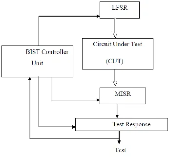
Figure 3.1 shows the BIST block diagra m. The signature of the circuit under test (CUT) is comparedwith the expected (refe rence) signature. If they bothmatch, the CUT is declared fault free , else it is declaredfaulty. Since several thousands of test responses are compactedinto a few bits of signature by an LFSR/MISR, there is an informat ion loss. As a result some faulty devices mayhave the same correct signature. The probability of a faultydevice having the sa me signature is called the probability ofaliasing. Thisprobability may be higher if the faults in the CUT are correlated.As a result there is no guarantee that the devicedeclared to be fault free is really fault free .
Fig. 1-BIST Bloc k Diagra m
Actual test selection depends upon the manufacturing level (processing,wafer, or package) being tested[6]. Although some testing is done duringdevice fabrication to assess the integrity of the process itself, most device testing isperformed after the wafers have been fabricated. The first test, known as wafer sortor probe, differentiates potentially good devices from defect ive ones . Afterthis, the wafer is scribed and cut, and the potentially good devices are packaged.Also, during wafer sort, a test site characterization is performed. Specia llydesigned tests are applied to certain test sites containing specific test patterns.These are designed to characterize the processing technology through measure mentof parameters such as gate threshold, polysilicon field threshold, bypass, metal fieldthreshold, poly and meta l sheet resistances, contact resistance[6], etc.
the sequence takes the circuit into the same or similar reach able states repeatedly. This is referred to as repeated synchronization. In addition, the on-chip test generation hardware consists of a single gate that is used for determining which tests based on will be applied to the circuit. The result is a simple an d fixed hardware structure, which is tailored to a given circuit only through the follo wing para meters.
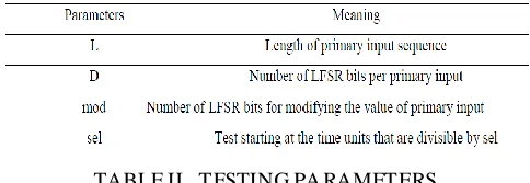
1) The number of LFSR bits.
2) The length of the prima ry input sequence .
3) The specific gates used for modifying the LFSR sequenceinto the sequence .
4) The specific gate used for selecting the functional broadsidetests that will be applied to the circuit based on . 5) Seeds for the LFSR in order to generate several primary input sequences and several subsets of tests.
The test generation hardware used in this paper has a simple and fixed structure, and it is independent of the number of sequences used. The sequences differ only in the seed used for the LFSR. The seeds can be stored on-chip, or a seed can be scanned in together with the initial state of the circuit before the application of every prima ry input sequence.When the circuit-under-test is embedded in a la rger design, its primary inputs may be driven by other logic blocks that are part of the same design. In addition, the primary inputs of the circuit-under-test include any external inputs of the design that drive the circuit-under-test. The primary outputs of the circuit-under-test may drive other logic blocks, or they may be prima ry outputs of the complete design. For simplicity this paper ass umes that primary inputs can be assigned any combination of values.
III FUNCTIONAL B ROADS IDE TES T
This section describes the on-chip generation of input patterns by using new efficient LFSR design based on the concepts discussed in Section II. Section III-A describes the generation of the input sequence using LFSR Section III -B describes the selection of tests that will be applied based on the number of input pins and fault level of the circuit. Section III-C describes the selection of parameter values in order to match the on-chip test generation hardware to a given circuit. The para meters of the on-chip test generation hardware are summa rized in Tab le I for ease of reference.
A.GENERATION OF INPUT PATTERN
The easiest way to generate input pattern is using binary counter. But this is very old technique and it takes a long time to detect faults. LFSR is an advanced version ,it gives ma ximu m randomness in the generation of patterns. Therefore within minimu m clock cycles ma ximu m nu mber of faults detected. Here an advanced LFSR is designed with some additional parameters. By using these parameters for a fixed hardware structure an LFSR can be designed.The basic parameters used in the design of LFSR is shown in TABLE II.
TABLE II. TESTING PA RAMETERS
Also the input patterns will initia lize the nets to a known sate. Once it enters into unreachable state , then the finite sta te machine will start operation with some unwanted states.For illustration, Fig.2 shows the hardware used for with
parameters.
Fig. 2-Input Pattern Generation
The 12-b it LFSR is shown at the top of Fig. 2. Here d=3 ,mod =2 and n=4 ,it is used fo r tests for input circuits such as S27 standard bench mark c ircu its. Bits 0, 1 and 2 of the LFSR are used for producing the values of I0 . Since , an OR
gate is used for increasing the probability that will be assigned the value 1. The OR gate is driven by bits 0 and 1 of the LFSR. Bit 2 of the LFSR reduces the dependencies between the values of and the values of I0 and I1 . Bits 3, 4, and 5 of
the LFSR are used for producing the values of I1. There fore, I1 is driven directly by bit 3 of the LFSR. Bits 4 and 5
reduce the dependencies between the values of and the values of I1 and I2 . Bits 6, 7, and 8 are used for producing the
values of I2. Since , an AND gate is used for increasing the probability that will be assigned the value 0. The AND gate
is driven by bits 6 and 7. Bit 8 of the LFSR reduces the dependencies between the values of I2 and those of I3 . Finally,
bits 9, 10, and 11 are used for producing the values of I3.Therefore, is driven directly by bit 9 of the LFSR. In general,
if there are prima ry inputs with , the imp le mentation illustrated by Fig. 2 requires a 12-b it LFSR, and AND or OR gates with mod inputs.
B.FAULT TES TING
The on-chip test generation hardware described so far has parameters L, mod,sel and d. These para meters determine the prima ry input sequence , and the tests that will be applied based on it. Keeping L, mod, d and sel constant in order to keep the hardware fixed, there is fle xib ility only in determin ing the seed of the LFSR. Diffe rent seeds yield different prima ry input sequences and different tests. Therefore, it is possible to increase the fault coverage by using several diffe rent seeds.
Fig. 3- 7 Input Co mb inational Circuit
Consider a 7 input combinational circuit in Fig.3. It is associated with 6 faults. Let F be the target fault list and here F contains;
2) Bridging fault 3) Short
4) OR gate is replaced by XOR gate 5) Stuck at one fault
6) Open
By applying suitable input patterns ,it is possible to detect the faults in each net one by one. As the pseudo random patterns having ma ximu m randomness ,then with minimu m cloc k cycles itself the maximu m fault coverage can be obtain. Also it leads to reduce the power dissipation. Therefore by every clock cycle the detected fault from the target list will e liminate and at the end,it is possible to make the target fault list empty.The efficiency of detection and elimination is completely based on the LFSR designed and the input patterns developed from it. If the input patterns are not capable to activate all the nets ,then it is not possible to detect errors in all nets.
C.S ELECTION OF PARAMET ERS
Increasing L and d can potentially increase the fault coverage. Increasing L increases the number of available tests, and increasing reduces the dependencies between the values of the prima ry inputs. Increasing sel can potentially decrease the fault coverage since it decreases the number of tests that will be applied to the circu it.
Increasing mod is not beneficia l always. Based on the number of input pins the selection of mod is determined .The values of the input parameters with determine the effectiveness of test patterns. If the test patterns are designed in highly effic ient manner then it is very easy to determine the target faults in min imu m c lock cycles. The target fault detection in earlier cycles will reduce the amount of power dissipation in the chip . This is also helpful to protect other circuits present in the IC . Otherwise by increasing power dissipation may cause unintended damage of co mponents.
Based on the values of parameters we can obtain the results as;
1)If the fau lt coverage does not exceed that of ordinary methods for any solution, we report on the followin g solutions. a) The solution with the highest fault coverage and thelowest number of seeds.
b) The solution with the highest fault coverage and thelowest number of applied tests.
2) If the fault coverage of at least one solution exceeds that ofbroad side t est, we report on the follo wing solutions. a) The solution with the highest fault coverage.
b) The solution with a fault coverage higher than that ofbroadside test and the lowest number of seeds. c) The solution with a fault coverage higher than that ofbroadside test and the lowest number of applied tests.
One of these solutions is expected to be the most appropriatefor the circuit. In addition to these solutions there are others with intermediate nu mbers of seeds and applied tests, which are not reported .
IV.RES ULT AND DISCUSS ION
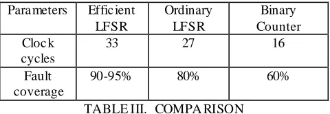
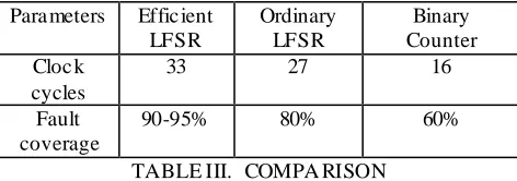
Based on this the application of different test patterns gives the f_list(target fault list) as shown in the Fig 4.As the number of input pins increases the comple xity of testing increases. Output contains the f_list based on binary counter, input patterns due to LFSR a lso with respect to efficient LFSR by selecting parameters.
Para meters Effic ient LFSR
Ordinary LFSR
Binary Counter Cloc k
cycles
33 27 16
Fault coverage
90-95% 80% 60%
TABLE III. COMPA RISON
Fig. 4- Simu lation Of 7 input Co mbinational Circuit
Para meters Effic ient LFSR
Ordinary LFSR
Binary Counter Cloc k
cycles
33 27 16
Fault coverage
90-95% 80% 60%
TABLE III. COMPA RISON
The Table III represents the comparison of different input generation methods based on clock cycles and fault coverage. Fro m the table it is clear that the Efficient LFSR design will give ma ximu m fault coverage with minimu m input clock cycles therefore it reduces the power consumption as compared to other methods of fault detection.
V. CONCLUDING REMARKS
This paper described a test generation method for functional broadside tests using efficient LFSR with selecting parameters. The hardware was based on the application of prima ry input sequences starting from a known reachable state, thus using the circuit to produce additional reachable states. Random primary input sequences were modified to avoid repeated synchronization and thus yield varied sets of reachable states. Two -pattern tests were obtained by using pairs of consecutive time units of the primary input sequences. The hardware structure was simple and fixed. Input patterns designed with selecting parameters will give ma ximu m output fault coverage with min imu m c lock cycles as compared with ord inary binary counter input sequence and LFSR rando m pattern generation. Also it reduces the power dissipation and increases the reliab ility of testing combinational circuits.
REFER ENC ES
[1] J.Rearick, “Too much delay fault coverage is a bad thing,” in Proc.Int.T est Conf., 2001, pp. 624–633.
[2] V. Gherman, H.-J. Wunderlich, J. Schloeffel, and M. Garbers, “Deterministic logic BIST for transition fault testing,” in Proc. Euro. T est Symp., 2006, pp. 123–130.
[3] I. Pomeranz and S. M. Reddy, “On reset based functional broadside tests,” in Proc. Design Autom. Test Euro. Conf., 2010, pp. 1438–1443. [4] I. Pomeranz, “Built-in generation of functional broadside tests,” presented at the Design Autom. T est Euro. Conf., Grenoble, France, 2011. [5] P. H. Bardell, W. H. McAnney, and J. Savir, Built-In Test for VLSI.
[6] Polian and F. Fujiwara, “Functional constraints vs. test compression in scan-based delay testing,” in Proc. Design, Autom. Test Euro. Conf., 2006, pp. 1–6.
[7] B. Konemann, “LFSR-coded test patterns for scan designs,” in Proc. Euro. Test Conf., 1991, pp. 237–242..