Vol. 4, Issue 7, July 2015
High Performance Conditional Push Pull
Pulsed Latches Using Dual Stack Approach
Shaik Khadar Sharif1, R.Sindhura2
Associate Professor, Dept. of ECE, VNR Vignana Jyothi Institute Engineering and Technology, Hyderabad, India1
PG Student [VLSI], Dept. of ECE, VNR Vignana Jyothi Institute Engineering and Technology, Hyderabad, India2
ABSTRACT: Latches and flip-flops are fundamental blocks for sequential circuits. New type of pulsed latches is introduced. Conditional push–pull pulsed latch is based on a push– pull final stage driven by two split paths with a conditional pulse generator. Two circuit implementations are discussed; the main difference in these two circuits is pulse generator, which can be either shared (CSP3L) or not (CP3L). Also the power consumption of these CP3L and CSP3L latches is further reduced by using the dual stack approach and delay will be approximately same. The performance for proposed topology is very fast, and outperforms the well-known transmission gate pulsed latch (TGPL) and TGPL is taken as reference circuit.Hence the proposed pulsed latch has the highest performance ever reported. Accordingly, the proposed class of pulsed latches goes beyond the current state of the art and it is well suited for VLSI systems that require high performance. The designs are simulated in tanner tools with a supply voltage of 1.8v at 180nm technology.
KEYWORDSClocking, energy efficiency, flip-flops, high speed, low power, pulsed latches, VLSI
I.INTRODUCTION
Flip Flops (FFs) and latches are responsible for a large fraction of the power budget in VLSI systems. Typically, theydissipate 80% of the total clock power, and 30% of the overall power budget. Now a days to get high performance using FFs and latchesis more critical than in past, considering speed can only increase through improvements in performance, since VLSI systems are power limited. Therefore, the novel topology with a targeted speed under relatively low power consumption iscrucial.Among latches and flip-flops, pulsed latches exhibit the best energy efficiency from moderate to highperformance design targets, among the existing classes of FFs. The transmission gate pulsed latch (TGPL) (see Fig. 1) usedin various Intel microprocessors is the most energy-efficient. Some other flip-flops such as STFF, TGFF gives low performance and low speed compared to TGPL. The TGPL will be taken as a reference circuit for high-speed and high performance designs. When slower designtargets are considered, master-slave FFs exhibitbetter energy efficiency. The traditional TGFF has better performance with more delay.
A new class of pulsed latches (conditionalpush–pull pulsed latch) is introduced to increase speed and performance. Two versions are presented, respectively, without (CP3L)and with (CSP3L) shareable conditional pulse generator.
II.PREVIOUS WORK
The existing work of this paper includes description of previous structure Transmission gate Pulsed Latch. The structure of Transmission Gate Pulsed Latch is shown in below figure.
CONDITIONAL PUSH–PULL PULSEDLATCH: MAIN IDEAS AND OPERATION.
In most existing technologies the pulsed latches shown in Fig. 2,a push–pull output stage is adopted (M7–M8) as opposed tothe traditional output inverter stage. This technique reduces the driving circuitryload, thereby it provides faster and high performance. It allows M7–M8 transistors in Fig.2 to be up-sized, and it provides a faster output stage. The output stage in Fig.2is driven by two split paths which generates the pulsed signals active-high R (active-low set
Vol. 4, Issue 7, July 2015
Fig.1: Schematic of TGPL
R and Sbar pulsesare alternatively generate the output for fall/rise transition and at the falling clock edge by using the conditional pulse generator these pulses are generated. These outputs are transferred to the next stage by using half latch M1–M3 or M4–M6, depending on input D, low or high. The half latches in the first stage contains the D–Q
critical path have less parasitic compared to clocked inverters or inverters with cascaded transmission gate (see M1–M4 in Fig. 2). It has two different paths which is driven by input D using NMOS (M5) and a PMOS (M2) transistor in Fig 6, and it is equivalent to the load of a input inverter stage (see M1–M2 in TGPL in Fig. 1).
Fig.2: Block diagram of the proposed class of pulsed latches.
The operation in Fig. 2 is explained in Fig. 3, the internalsignals are also added in the main waveform. If previous output QD is high or low will be checked by using pulse generator after the falling clock edge.The next output Qcan stay at the same value or make a falling transition(cycle 1in fig 3) if previous output QD=1, and it generates a pulse in
the fall path in Fig. 2 through theCPf, otherwise nothing changes in the risepath (CPris kept low, thus latch M4–M6 transistors keeps Sbarhigh and M8 OFF). If input D=1stays at the previous value, the latch M1–M3 is OFF; and R
should be kept at the previous valueR = 0. If input changes to D = 0, the latch M1–M3 is ON and a highpulse in R is
determinedbyCPf,and M7 transistor is ON and brings the output Q tolow. Afterwards, the QD experiences same transition as Q but with some delay.
A pulse is generated in the rise path through the CPr(cycle 2 in Fig. 3)based onprevious output QD=0 after the falling clock edge(nothing changes in thefall path). If inputD = 0stays at the previous value, the latchM4–M6 is disabled and
Sbaris high, and there is no change in the rise path. If input changes to D = 1, the latch M4–M6 is ON and the pulse
Vol. 4, Issue 7, July 2015
Fig.3: Waveforms of internal signals of the general scheme in Fig. 2
The output is maintained at the desired value by the keeper by turning of the M7-M8 transistors at the steady state, R
(Sbar )in Fig. 2 is set to 0 (1). The keeper which is the memory element in Fig. 2 is placed at the output node because in first stage the half latch need to drive only single transistor, but in other topologies it is placed before the outputstage and we can observe in TGPL. These permits to move the parasitic associated with the memoryelement to the output node, thereby making the output stage lightly loaded and hence faster and moreenergy efficient.
III.IMPLEMENTATION OF PROPOSED TOPOLOGIES
As we discussed above pulsed latch in Fig. 3 have lightly loaded D–Q critical path, and it makes potentially fast and energy-efficient. Thesefeatures can be implemented in different ways. In thefollowing two versions are presented without (Section III-A) and with (Section III-B) shareable pulsegenerator.
A.CONDITIONAL PUSH–PULL PULSED LATCH
The CP3L schematic is shown in Fig. 5.The output Q is driven by the keeper and it contains cross coupled inverter pair, and the forward inverter is used to avoid current contention. Output stage in the pull-down network is ON and pull-up network of keeper is OFF if R = 1. Analogously, the output stage of the pull-up is ON and pull-down of keeper is OFF if Sbar= 0
Vol. 4, Issue 7, July 2015
The R and Sbar pulsesare alternatively generated, through M10 or M11 in the keeper is actually subject to transitionsof the gate terminal in a given cycle. In contrast, the first stagemust drive two transistors associatedwith the keeper, and both of them are subject to transitions (see transistors M11–M12 in Fig. 1, which loadtransistors M3–M4 lying in the critical path). This reduces the parasitic load in the first stage of CP3L and reducesactivity at the keeper capacitances, thereby making the first stage faster.
Fig 5 Clock phase generator
Pulse generatorconsists of a clock phase generator, pseudo-NAND/NOR gates for the fall/rise paths. Generally, the CPf/CPr signals should be high or low based on pseudo-NAND/NOR gates and the clock signals CK (I and IV) is complementary with the CK(0and III) and each inverter is assumed to have the same delay τinv. The width of CPfand CPrpulsesdetermines the width of the transparency window of CP3Llatch in which the input can affect the output. The transparency window width can bemodified by changing the inverter delay in clock phase generator in Fig. 5. Almost all pulsed latches adopt thesame pulse generator topology. The delayed QD is kept stable as its previous value during the transparency window; it prevents glitches in CPr/CPfand reduces dynamic energy.
The output Q is connected directly to the pseudo-NAND/NOR without the delay stage in Fig.4, hence any outputtransition within the transparency window immediatelytriggers the generation of an additional (undesired) pulse.Ifdelay stage is not inserted in the feedback path the glitch occurs in CPr but it doesn’t affect the output. The delay stage is not strictly necessary, but its insertion of delay provides better results.
B. CONDITIONAL SHAREABLE PUSH–PULL PULSED LATCH
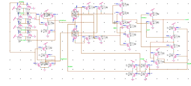
Here we present a different implementation with same concept and the total pulse generator is shared by adding a conditional logic. But in CP3L, the pulse generator cannot be shared amongmultiple latches since pseudo-NOR/NAND are driven by QD,which is different for each latch. The schematic of conditional shareablepush–pull pulsed latch (CSP3L) is shown in Fig. 6
Vol. 4, Issue 7, July 2015
In CP3L pseudo NAND/NOR gates used but in case of CSP3L in shareable pulse generator static NAND/NOR gates are used to generate the pulses which is CPf,ext andCPr,extand have thesame role as CP f and CPrhad in CP3L. The external pulses are coming from sharable pulse generator. The conditional pulse selection logic consists of two transmissiongates and two small keepers to maintain the same operationas before. The extra delay is added in the feedback because the transmission gates need complementary control signals.
The operation is similar to CP3L but the main difference is in conditional pulse selection logic and it enables the pulses according to the delayed output QD.Based on QD (1 or 0) the rise/fall paths will be enabled and it transfers the pulses to the next stage which is similar to the CP3L. A small difference from CP3L, the input capacitance seen fromexternal pulses in CSP3L depends on Q, which may leadto data-dependent clock skew. In practical cases, this is not possible.
IV.DUAL STACK TECHNIQUE
A variation of the sleep approach is the zigzagapproach, the overhead caused by sleeptransistors is reduced by placing alternating sleep transistors. Another technique for powerreduction is the stack approach, which breaks down an existing transistor into two half Size transistor by using stack effect then sleep transistors areadded in parallel to one of the divided transistors.
During sleep mode, sleep transistors are turned offand stacked transistors suppress leakage current whilesaving state. Each sleep transistor, placed in parallel to the one of the stacked transistors, reducesresistance of the path, so delay is decreased duringactive mode. However, area penalty is aNMOS significant matter for this approachNMOS once every transistor is replaced by threetransistors and NMOS once additional wires are addedfor S and S’, which are sleep Signals. Anothertechnique called Dual stack approach uses theadvantage of using the two extra pull-up and twoextra pull-down transistor NMOS in sleep mode eitherin OFF state or in ON state. NMOS once the dualsleep portion can be made common to all logiccircuitry, less number of transistorNMOS is needed toapply a certain logic circuit.
Fig.7: Dual-Stack approach
This dual stack approach is implemented to the above conditional push- pull latches and the new designs are proposed and are shown in figures 8 and 9.
Vol. 4, Issue 7, July 2015
Fig.9: CSP3L with dual stack technique
V. SIMULATION RESULTS
The simulation of all above designs is carried out by using Tanner EDA tool v13.0 with 180nm technology. The simulated waveforms of existing and proposed TGPL, CP3L, and CSP3L are given in below figures:
Fig.10: Simulated waveforms of TGPL design
The above fig:10 contains the clk and D are the inputs and Q is the output. In this figure clk operates in rising edge the output Qwill be based on D input.
Fig.11: Simulated waveforms of CP3L design
Vol. 4, Issue 7, July 2015
Fig.12: Simulated waveforms of CSP3L design
Both the fig:11 &12 the clk will be operated in falling edge and the output Q will be based on D input and delayed Qd
which will acts as another input. If D=0, Qd=0 or 1 then Q=0. If D=1, Qd=0 or 1 then output Q=1 based on CPf and CPr.
Fig.13: Simulated waveforms of CP3L Dual Stack design
Dual stack techniques for CP3L and CSP3L are mainly used to reduce power dissipation and delay. In dual stack technique all the vdd and gnds can be removed and places dual stack transistors and connects to single vdd and gnd
Fig.14: Simulated waveforms of CSP3L dual stack design
Both the fig: 13& 14 the clk operates at the falling edge and if D=0 and Qd=0 or 1 output Q=0.if D=0, Qd=1 or 0 then
Vol. 4, Issue 7, July 2015
PERFORMANCE COMPARISION
Table.1: Performance comparison table of different designs
TGPL CP3L CSP3L CP3L
dual
stack
CSP3L
dual
stack
Power
dissipat
-ion(w)
138µ 114µ 104µ 111µ 101µ
Delay(
sec)
3.22n 2.32n 2.34n 2.31n 2.34n
From the above comparison the CP3L and CSP3L dual stack techniques is having high performance (means less power dissipation and delay)and TGPL is having less performance.
VI. CONCLUSION
In this paper, a new class of pulsed latches has been introduced. Its push–pull final stage and split paths in the first stage enable a significant reduction in path and parasitic effort. Also the dual stack transistor method is applied to these pulsed latches to improve the performance by reducing the power consumption. All designs are simulated in Tanner tool with 180nm CMOS technology and the comparison results are tabulated.
The future activities may include other sequential designs using pulsed latches with high performance
REFERENCES
[1] S. Naffziger and G. Hammond, “The implementation of the next generation 64b itanium microprocessor,” in Proc. IEEE ISSCC, pp. 276-504, Feb. 2002,
[2] B. Dally,“Architectures and circuits for energy-efficient computing,” inProc. CICC, pp. 1–10.Sep. 2012,
[3] M. Alioto, E. Consoli, and G. Palumbo, “Flip-flop speed/performanceversus clock slope and impact on the clock network design,” IEEE Trans.Circuits Syst., vol. 57, no. 6, pp. 1273–1286, Jun. 2010.
[4] C. Giacomotto, N. Nedovic, and V. Oklobdzija, “The effect of the system Specification on the selection of clocked storage elements,” IEEEJ Solid-State Circuit, vol. 42, no. 6, pp. 1392–1404, Jun. 2007.
[5] T. Fischer, S. Arekapudi, E. Busta, C. Dietz, M. Golden, S. Hilker,A. Horiuchi, K. A. Hurd, D. Johnson, H. McIntyre, S. Naffziger, J. Vinh,J. White, and K. Wilcox, “Design solutions for the Bulldozer 32nm SOI2-core processor module in an 8-core CPU,” in IEEE ISSCC Dig. Tech.Papers, pp. 78–80,Feb. 2011.
[6] P. Gronowski, W. Bowhill, R. Preston, M. Gowan, and R. Allmon,“High-performance microprocessor design,” IEEE J. Solid-State Circuits, vol. 33, no. 5, pp. 676–686, May 1998.