Available online: https://edupediapublications.org/journals/index.php/IJR/ P a g e | 1128
PALAPARTHI.BUJJIBABU
ASSISTANT PROFESSOR Dept. of E.C.E
MALINENI LAKSHMAIAH WOMENS ENGENERING COLLEGE
GUNTUR DT.
ABSTRACT—
A parallel-prefix adder gives the best performance in VLSI design. However, performance of existed adder through black cell takes huge memory. So, gray cell can be replaced instead of black cell which gives the Efficiency in proposed Adder. The proposed system consists of three stages of operations they are pre-processing stage, carry generation stage, post-processing stage. The pre-post-processing stage focuses on propagate and generate, carry generation stage focuses on carry generation and post-processing stage focuses on final result. In ripple carry adder each bit of addition operation is waited for the previous bit addition operation. In efficient proposed adder, addition operation does not wait for previous bit addition operation and modification is done at gate level to improve the speed and to decreases the memory used.Key Words: Parallel Prefix Adder, Kogge stone Adder, Carry Select Adder
I.INTRODUCTION
The important component in most digital circuit styles together with digital signal processors and micro chip information path units is the binary adder. As such, intensive analysis continues to be targeted on raising the facility delay performance of the adder [1]. Parallel-Prefix adders are glorious to own the most effective performance in Very Large Scale Interagation. Field Programmable Gate Arrays is a configurable logic which has improved its quality in recent years as a result of which the speed and power over DSP-based and microprocessor-based solutions for several sensible styles has been improved
involving mobile DSP, telecommunication
applications, of which it results a reduction in development time and price over Application Specific computer circuit styles. The facility advantage is particularly vital with the growing
quality of mobile and moveable physical science, that create intensive use of DSP functions.
However, the structure of the configurable logic and routing resources in Field Programmable Gate Arrays and parallel-prefix adders has a special performance than Very Large Scale Integration implementations. Specifically, most up-to-date Field Programmable Gate Arrays use a fast-carry chain that optimizes the carry path for the straightforward Ripple Carry Adder. In this paper, the coming up concerned
sensible problems are delineated with the
implementing tree-based adders on Field
Programmable Gate Arrays. Associate degree economical testing strategy for evaluating the performance of those adders is mentioned [3]. Many tree-based adder structures are enforced and characterized on a Field Programmable Gate Arrays and compared with the Ripple Carry Adder and also the Carry Skip Adder. Finally, some conclusions and suggestions for rising Field Programmable Gate Arrays styles to change higher tree-based adder performance are given.
The working principle of the Arithmetic Logic Units is to calculate the data which was send to the ALU. In general, we can calculate the values line by line or in the order. It will take some more time than the actual time. There will be lot of time is consuming in the process. To rectify this problem, a new technique has been introduced in the digital computer system. That is Parallel Prefix Adder. Adders are the important components in the digital computer systems due to their fast functionality in their work. The main purpose of these adders is to calculate the address in quick time. Among all the adders Parallel Prefix Adder is the main useful adder. Adders are to calculate the address and the give the solutions to the problems in no time. Kogge Stone
GONUGUNTLA.MOUNIKA
M.TECH – SCHOLAR – E.C.E Dept. of E.C.E
MALINENI LAKSHMAIAH WOMENS ENGENERING COLLEGE
Available online: https://edupediapublications.org/journals/index.php/IJR/ P a g e | 1129 Adder is one of the common types of parallel prefix
adder. Kogge – Stone adder has been developed by Xilinx 14.1 software which is more advantageous and more developed.
If the complete operation is leaded by the inputs of the initials, that is called prefix. If the execution of the operation is been in parallel condition it is called parallel. This will be done by making the operation into some small pieces. The main advantage in this technique is that the operation or the calculation part will be completed in parallel direction. The former calculating techniques will make the calculations in one by one process. But in this technique the calculations will be calculated in parallel condition. Then there will be lot of time can be saved.
II.EXISTED SYSTEM
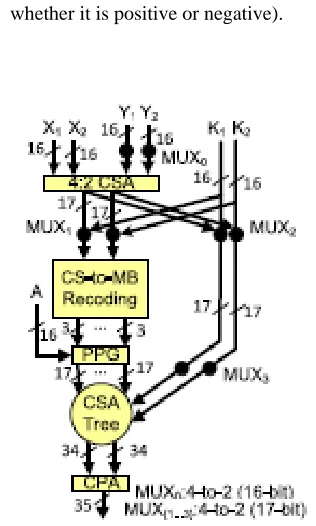
This proposed system incorporates the CS-to-MB recoding unit. We assume 16-bit input operands for all the designs and, without loss of generality; we do not consider any truncation concept during the multiplications. A carry-save adder is a type of digital adder, used In computer micro architecture, to compute the sum of three or more n-bit numbers in binary a type of digital is used that is carry
save adder.
It differs from other digital adders in that it outputs two numbers of the same dimensions as the inputs, one which is a sequence of partial sum bits and another which is a sequence of carry bits. Using basic arithmetic. Although we know the last digit of the result at once, we cannot know the first digit until we have gone through every digit in the calculation, passing the carry from each digit to the one on its left. To take a time proportional to n add two n digit numbers, even if the machinery we are using would otherwise be capable of performing many calculations simultaneously.In electronic terms, using bits (binary digits), this means that even if we have n one-bit adders at our disposal, to allow a possible carry to propagate from
one end of the number to the other a time proportional to n is required. Until we have done this,
1. We do not know the result of the addition.
2. We do not know whether the result of the addition is larger or smaller than a given number (for instance, we do not know whether it is positive or negative).
Fig. 1.
Incorporating the CS-to-MB
recoding concept
A carry look-ahead adder can reduce the delay. In principle the delay can be reduced so that it is proportional to logn, but for large numbers this is no longer the case, because even when carry look-ahead is implemented, the distances that signals have to travel on the chip increase in proportion to n, and propagation delays increase at the same rate.A carry look-ahead is not of much use in public key cryptography, once we get the 512bit to 2048 bit number sizes that is required.
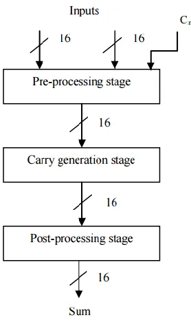
III.PROPOSED SYSTEM
Available online: https://edupediapublications.org/journals/index.php/IJR/ P a g e | 1130 network and post-processing. Pre-possessing stage is
to calculate, produce and spread the signals. Carry generation network is to calculate the values in parallel level and these calculations will be segmented in minute pieces. Finally, the Post-processing stage is to complete the calculation part by collecting all the bits.
Carry look-ahead Adder: The main theme of this carry look-ahead adder is, to attempt and generate all incoming bits in parallel.
Pre-Processing Stage: Generate and propagate are from each pair of inputs in the pre-processing stage. The propagate gives “XOR” operation of input bits and generates gives “AND” operation of input bits [7]. The propagate (Pi) and generate (Gi) are shown in below equations.
Fig. 1. Block Diagram
Carry Generation Stage
In this stage, carry is generated for each bit and this is called as carry generate (Cg). The final cell present in the each bit operation gives carry and for further operation the carry propagate and carry generate is generated.The last bit carry will help to produce sum of the next bit simultaneously till the last bit. The
carry generate and carry propagate are given in below equations.
The above carry propagate Cp and carry generation Cg in equations 6&7 is black cell and the below shown carry generation in equation 8 is gray cell. The carry propagate is generated for the further operation but final cell present in the each bit operation gives carry. The last bit carry will help to produce sum of the next bit simultaneously till the last bit. This carry is used for the next bit sum operation, the carry generate is given in below equations 8.
Post-processing stage:
It is the final stage of an efficient P.P.A adder, the carry of a first bit is XORed with the next bit of propagates then the output is given as sum and it is shown in equation.
Each bit carry undergoesthe post-processing stage with propagateand used for two sixteen bit addition operations which gives the final sum.
The first input bits goes under pre-processing stage and it will produce propagate and generate. The carry generates and carry propagates are produced by carry generation stage with the help of propagates and generates which undergoes post-processing stage to give the final sum. The step by step process of efficient P.P adder.
The Efficient P.P adder structure is looking like tree structure for the high performance of arithmetic operations and it is the fastest adder which focuses on gate level logic. It designs with less number of gates. So, it decreases the delay and memory used in this architecture.
Available online: https://edupediapublications.org/journals/index.php/IJR/ P a g e | 1131 cells are active in low inputs and produce the active
high outputs. And second cells are active in high inputs and low outputs.
Parallel prefix adder has the lower delay of power when compared with other adders. Power will be saved by using this method than that of other methods. This is more suitable design and method for Arithmetic Logic Unit to work properly and accurately. It is also useful for yielding good performance in the calculating the data.
IV.RESULTS TECHNOLOGY SCHEMATIC
OUTPUT WAVEFORM
V.CONCLUSION
In this paper, a new approach to design P.P adder concentrates on gate levels to improve the speed and decreases the area.It is like tree structure and cells in the carry generation stage are decreased to speed up the binary addition. The great advantage in reducing delay is offered by the proposed adder addition operation.
VI.REFERENCES
[1] Padmajarani, S. V., and M. Muralidhar. "A New Approach to implement Parallel Prefix Adders in an FPGA." (2012): 1524-1528.
[2] JianhuaLiuZhu, Haikun, Chung-Kuan Cheng, John Lillis, “Optimum prefix Adders in a Comprehensive Area,Timing and power Design Space”., Proceeding of the 2007 Asia and South pacific Design Automation conference.Washington, pp.609-615,jan 2007.
[3] Taeko Matsunaga and Yusuka Matsunaga., “Timing-Constrained Area minimization Algorithm for parallel prefix adders”, IEICE TRANS, Fundamentals, vol.E90-A, No.12 Dec, 2007.
[4] Hoe, David HK, Chris Martinez, and Sri JyothsnaVundavalli. "Design and characterization of parallel prefix adders using FPGAs." System Theory (SSST), 2011 IEEE 43rd Southeastern Symposium on. IEEE, 2011.
[5] GiorgosDimitrakopoulos and DimitricNikolos, “High Speed Parallel –Prefix VLSI Ling Adders”, IEEE Trans on computers, Vol.54, No.2, Feb 2005 [6] Pakkiraiah. Chakali, madhu Kumar. Patnala “Design of high speed Ladner - Fischer based carry select adder” IJSCE march 2013
[7] HaridimosT.Vergos, Member, IEEE and
GiorgosDimitrakopoulos, Member, IEEE,” On modulo 2n +1 adder design” IEEE Trans on computers, vol.61, no.2, Feb 2012
[8] David h, k hoe, Chris Martinez and Sri Jyothsnavundavalli “Design and characterization of parallel prefix adders using FPGAs“, Pages.168-172, march2011 IEEE.
[9] K. Vitoroulis and A.J. Al-Khalili, “performance of parallel prefix adders implemented with FPGA technology,” IEEE Northeast Workshop on circuits and systems, pp.498-501, Aug 2007.
[10] GiorgosDimitrakopoulos and DimitrisNikolos, “High Speed Parallel Prefix ...Ling adders," IEEE Transactions on Computers, vol.54, no.2, February 2005
[11] S. Knowles,” A family of
Available online: https://edupediapublications.org/journals/index.php/IJR/ P a g e | 1132
PALAPARTHI.BUJJIBABU
studied B.Tech at RVR&JC
college of engineering and
M.Tech at Godavari institute
of
engineering
and
technology. At present he is
working
as
assistant
professor
at
malineni
lakshmaiah
women’sengineering college
with 8 years of experience.
His area of interest is digital
electronics.
GONUGUNTLA MOUNIKA
studied B.Tech at Sri Mittapalli college ofengineering during 2011-2014.At present she is pursuing M.TECH atMalineni lakshmaiah