Design and Implementation of Dual Mode
Logic Based Phase Locked Loop with Sleepy
Stack Approach
Neelima Koppala
1, P. Uma Maheswari
2, Charan Kumar K
3Assistant Professor, Department of ECE, Sree Vidyanikethan Engineering College, A.Rangampet, Tirupati, Andhra
Pradesh, India 1,2,3
ABSTRACT: - This paper deals with Type-I Phase Locked Loop designed for an operating frequency of 1MHz, capture to lock frequency ratio as 0.63. Further the design is extended with low power techniques which aim at reducing the leakage power of the design. Two low power novel techniques called sleepy stack approach and dual mode logic are used. The existing design is modified with these two approaches and their combination for low power designs. The designs are simulated in HSPICE synopsis tool and the waveforms are verified in Avanwaves tool. The proposed design of PLL using both dual mode logic and sleepy stack approach reduces the power dissipation by nearly 95% when compared to the existing design. Hence the low power PLL is best suited for practical applications as it doesn’t deviate much from the specifications.
KEYWORDS: Type-I PLL, Sleepy Stack Approach, Dual Mode Logic, VCO, Phase detector.
I. INTRODUCTION
A PLL [1] is a feedback system that includes a VCO, phase detector, and low pass filter within its loop. Its purpose is to force the VCO to replicate and track the frequency and phase at the input when in lock. The PLL is a control system allowing one oscillator to track with another. It is possible to have a phase offset between input and output, but when locked, the frequencies must exactly track.
The PLL [2] output can be taken from either Vcont, the filtered (almost DC) VCO control voltage, or from the output of the VCO depending on the application. The former provides a baseband output that tracks the phase variation at the input. The VCO output can be used as a local oscillator or to generate a clock signal for a digital system. Either phase or frequency can be used as the input or output variables as shown in figure 1.
Figure 1: Block Diagram of PLL
The basic applications of PLL include Clock Generation, Frequency Synthesizer, Clock recovery in a serial data link, etc.
II. EXISTING PLL
The PLL is designed with the following specifications i.e., for Wideband FM with operating frequency f0=1MHz,
kf=250kHz/V, kd=0.1 V/rad, R=10KΩ, C=1000pF, the lock range frequency is f_lock = kf*kd*pi/2 = 39kHz, and the
corresponding voltage lock value is v_lock = kd*pi/2 = 0.157. The capture to lock range is f_capture/f_lock ~=
1/sqrt(2*pi*R*C*f_lock) = 0.63, the corresponding capture potential is v_capture ~= 0.100.
III. LOW POWER TECHNIQUES
In this paper, two low power techniques are used i.e., Sleepy Stack approach and Dual Mode Logic. Both of these techniques aim at reducing the power dissipated. Also the sleepy stack approach is designed to reduce the leakage power.
A. Sleepy Stack approach
B. Dual Mode Logic
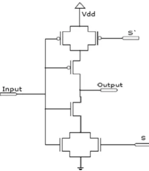
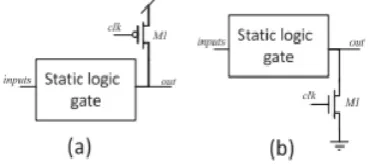
The basic DML (Dual Mode Logic) gate is having an normal static logic gate, which can be an conventional CMOS logic gate and at the output side we are connecting an normal transistor. And whose gate is connected to a global clock signal is applied to it as switching circuit. The whole operation is based upon the external connected transistor and its clock signal speed. The DML [5] can be arranged as two ways depending upon the type of transistor using at the output side either PMOS or NMOS transistor as following way shown in the figure 3.
Figure 3: DML Topology (a) Type A (b) Type B
The DML [6] provides the designer with a very high flexibility to overcome the disadvantages of the following two methods – 1) static mode and, 2) dynamic mode. Since, in static mode of operation the power dissipation is low and speed is also very low compared to the dynamic mode. Similarly in dynamic mode the speed is very high and power dissipation is also high compared with static mode.
IV. PERFORMANCE & DIFFERENCE BETWEEN EXISTING AND PROPOSED PLL DESIGNS
The PLL is designed in four ways i.e., with (i) existing technique, (ii) Sleepy Stack approach (iii) Dual Mode Logic and (iv) both sleepy stack and dual mode logic.
In the existing design, the power is obtained in terms of mW. In sleepy stack approach, as the technique is applied to only PLL, the design doesn’t vary much with existing design. In dual mode approach using type B, the design slightly decreases the power dissipation. But with the combination of both dual mode logic and sleepy stack approach, the power is reduced drastically as shown in table 1.
Table 1: Comparison in terms of Power dissipation
PLL Design Power Dissipation
(W)
Existing PLL 2.4749E-03
Sleepy Stack based PLL 2.4749E-03
DML based PLL 2.4328E-03
DML based PLL with Sleepy Stack
Figure 4: Graphical comparison of Power dissipation of existing and proposed PLL designs.
The graphical representation is shown in figure 4. From figure 4 and table 1, it is shown that the design of PLL with DML logic reduces by 2% but in combination with sleepy stack approach, it reduces by 95% when compared with existing PLL design.
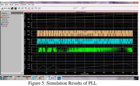
IV. RESULTS
Figure 5: Simulation Results of PLL
VI. CONCLUSION
The PLL is designed for an operating frequency of 1MHz, capture to lock frequency ratio as 0.63 using low power techniques like sleepy stack approach and dual mode logic. The existing design is modified with these two approaches and their combination for low power designs with reduction in overall power dissipation. The low power designs aim at reducing the leakage power and increase the speed. The designs are simulated in HSPICE synopsis tool and the waveforms are verified in Avanwaves tool. The proposed design of PLL using both dual mode logic and sleepy stack approach reduces the power dissipation by nearly 95% when compared to the existing design, which makes it suited for practical applications like clock generation, frequency synthesizer,etc.
REFERENCES
[1] Levi I,Ben, Beer-Sheva,, Fish. A, “High Speed CMOS Charge Pump Circuit for PLL Applications Using 90nm CMOS Technology”, Middle-East Journal of Scientific Research, ISSN 1990-9233, 2012, pp.1584-1590.
[2] Yashpal Sen, Nitin Jain, “Design and Implementation of Pahse Locked Loop using Current starved Voltage Controlled Oscillator”, Advance in Electronic and Electric Engineering, ISSN 2231-1297, Vol.4, No.0, 2014, pp. 637-644.
[3] C.jagadesssh, R.Nagendra, Neelima Koppala, “Design & Analysis of Different Types of sleepy Methods for Future Technologies”, International Journal of Engineering Trends and Technology (IJETT), ISSN 2231-1297, Vol.4, Issue 4, April 2013, pp. 1273-1278.
[4] Ajay Kumar Dadoria, Kavita Khare, “A Novel Approach For Leakage Power Reduction Techniques In 65nm Technologies”, International Journal of VLSI Design & communication Systems (VLSICS), Vol.5, No.3, June 2014, pp. 1-11.
[5] Levi I,Ben, Beer-Sheva,, Fish. A, “Logical Effort for CMOS –based Dual Mode Logic Gates”, IEEE Transactions on VLSI Systems, ISSN 1063-8210, Vol. 22, Issue 5, May 2014, pp.1063-8210.