IJEDR1504129
International Journal of Engineering Development and Research (www.ijedr.org)744
Design of High performance and Low Power 8T Full
Adder Cell Using Double Gate MOSFET at 45nm
Technology
1Shalini,2Mrs. Deepti Malhotra 1Department of electronics and communication
1KUK University Kurukshetra,India
________________________________________________________________________________________________________
Abstract - Design of complex arithmetic logic circuits considering active power and delay is an important and challenging task in deep submicron circuits. Double gate transistor circuit consider as a promising candidate for low power application domain as well as used in Radio Frequency (RF) devices. In this paper we designed full adder with the help of double gate transistor, the used parameters value has been varied significantly thus improving the performance of full adder. Power Gating is one of the most used circuit techniques to reduce the leakage current in idle circuit. In this paper different parameters are analysed on Power Gating Technique. Power Gating technique achieves 93% reduction of leakage current, active power is reduced by 65% and delay is reduced by 24% as compared with conventional double gate full adder. Simulation results of double gate full adder have been performed on cadence virtuoso with 45nm technology.
Keywords - Power Gating, Double-gate MOSFETs, full adder, Power, Delay.
________________________________________________________________________________________________________
I. Introduction
Life of battery is the most important factor in portable electronics devices. An adder is the most important component of an arithmetic unit. The efficiency of arithmetic unit is depending on the efficiency of adder. To improve the performance in terms of low power and high speed of an adder many structure are designed. Adder is the critical and most essential building blocks in DSPs and microprocessors. In this paper we present a 8T full adder circuit by using double gate MOSFET which consume low power and give faster response. In the proposed adder circuit we use 8 double gate transistors so it is called 8T adder cell. We used 8T adder because it required less area as compared to the higher gate count full adders, lower power consumption and low operating voltage 5v-7v. It is difficult to keep full voltage move forward and backward operation with transistor count and low power consumption are pursued. In transistor logic circuit, the output voltage move forward and backward may be degraded due to threshold problem. The disadvantage of 8T full adder circuit is loss of threshold voltage in transistors. To overcome this drawback circuit design in this paper. Double gate MOSFET technique reduces power consumption, area and transistor stack height. In double gate MOSFET, there are two electrically independent gates, which give more flexibility in design of low power. To reduce short channel effect of scaled device Double gate transistor is used due to their better electrostatic control on channel charges. As compared to the conventional structure 8T structure saves up to 84% of the number of transistor involved in the conventional full adder so the area required by 8T structure is reduced. The power consumption for CMOS circuit is given by the following equation :
𝑃𝑎𝑣𝑔 = 𝑃𝑑𝑦𝑛𝑎𝑚𝑖𝑐+ 𝑃𝑙𝑒𝑎𝑘+ 𝑃𝑠ℎ𝑜𝑟𝑡 𝑐𝑖𝑟𝑐𝑢𝑖𝑡 (1)
We clearly say that the power depend on the different parameter as well as on the supply voltage. Lowering the supply voltage would significantly lower the power consumption of the circuit. This basic concept of would be used to improve the performance of adder circuit.
II. STRUCTURE OF DOUBLE GATE AND BENEFITS
In double gate MOSFET (DGMOSFET), Si channel is very small in width and can be controlled by applying gate control on both sides of channel. In double gate device both gate are coupled each other and this reduce the short channel effect and leakage. By using two gates circuit with double gate transistor can be operated as low input voltage as compared to the planer CMOS circuit and these means low power consumption. Gate leakage is also low in double gate device. It is occur due to gate tunnelling and overlap tunnelling current. Here short channel effect is controlled by two gates so there is no need to heavy doping. Since very light doped or undopped channel can be used in double gate transistors.
III. FULL ADDER
IJEDR1504129
International Journal of Engineering Development and Research (www.ijedr.org)745
Full adder is a combinational circuit addition operation of input bits. Full adder contains three inputs and two outputs. The input variables are A, B and Cin. The two output variables are SUM and carry (Cout). The Boolean expression for full defined below:𝑆𝑈𝑀 = (𝐴 𝑥𝑜𝑟 𝐵 𝑥𝑜𝑟 𝐶) (2)
𝐶𝐴𝑅𝑅𝑌 = (𝐴 𝑎𝑛𝑑 𝐵) 𝑜𝑟 (𝐴 𝑎𝑛𝑑 𝐶) 𝑜𝑟 (𝐵 𝑎𝑛𝑑 𝐶) (3)
IV. PROPOSED FULL ADDER
In this we have proposed full adder circuit which shows better results as compare to given circuit. The four-transistor XNOR module has been used in this full adder. XNOR signal is used as the selector of two static multiplexer. XNOR signal has Vt threshold loss. Output multiplexers have Vt threshold loss too. COUT and SUM generator circuits are two multiplexers that each uses only two transistors. There are not any VDD and GND in these components therefore these components consumes low power. Simplicity of the carry generator and sum generator circuits are another reason to decrease power and delay in these circuits. The main problem of the circuit is output threshold loss problem. The total number of transistors used in this circuit is ten. There is semi inverter to invert input A. This inverter should work only when XNOR signal is equal to logic 0. Therefore, we use XNOR signal as GND of the inverter to decrease short circuit and leakage power in the inverter. On the other hand, switching activity on the node X will be reduced by using XNOR signal in the mentioned inverter. Input C, drive one transistor gate and two transistor junctions. The schematic of 4T XNOR circuit is shown in Figure 1 and Figure 2 shows a truth able of XNOR circuit. This is heart of full adder circuit.
Fig.1:4T XNOR circuit
Fig.2: Truth table
a) Block diagram and truth table
The block diagram and truth table for proposed circuit is shown in this section. The block diagram tells how the circuit works and implementation of proposed circuit is verified by given truth table. The Figure 3 and 4 shows block diagram and truth table respectively.
Fi.3: Block diagram
Fig.4: Truth table for proposed circuit
IJEDR1504129
International Journal of Engineering Development and Research (www.ijedr.org)746
In double gate MOSFET (DGMOSFET), Si channel is very small in width and can be controlled by applying gate control on both sides of channel. In double gate device both gate are coupled each other and this reduce the short channel effect and leakage. By using two gates circuit with double gate transistor can be operated as low input voltage as compared to the planer CMOS circuit and these means low power consumption. Gate leakage is also low in double gate device. It is occur due to gate tunnelling and overlap tunnelling current. Here short channel effect is controlled by two gates so there is no need to heavy doping. Since very light doped or undoped channel can be used in double gate transistors .Double gate 10t full adder circuit
Double gate Transistor can be constructed by connecting two transistors in parallel as a manner that their source and drain are connected together. Double gate transistor can be designed by two gate structure, based on gate biasing, first one is achieved by independent gate control and it is described as four terminal devices. When the front and back gate are connected together second one is implemented abd it is described as three terminal devices, this structure is used for direct replacement of single gate transistor.
Fig 5:Double gate 10T transistor full adder
VI. REDUCTION TECHNIQUE
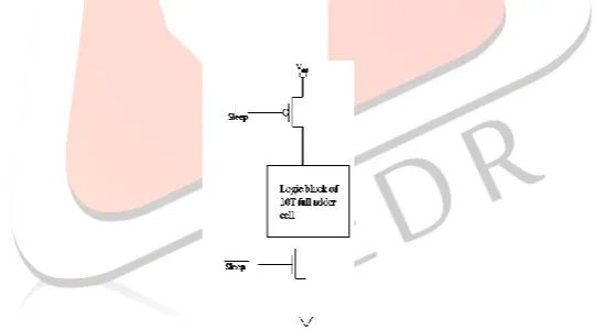
Power Gating
Power Gating, it reduces the leakage by inserting n-MOS and p-MOS to the circuitry. Figure shows the power Gating circuit. This technique is very popular for reducing leakage in the circuits. Because of simplicity implementation of the technique, power gating has been used to minimize leakage energy in circuits at architectural level. The effectiveness of power gating required following
Fig.6: Power Gating Circuit.
It provides the switches for turning off and on of the functional units at circuit level.
These switches controls the power g ate at various parts of the circuit can be provided as handles at the system software or the level thereby giving the system compiler the ability to control them.
A sleep control mechanism is used for efficient power management. In the active mode, sleep is set to low and sleep controlled transistor is turned on. Since their resistance is small the supply voltage Vdd and Vss(gnd) function as real power line. In standby mode, sleep is set to high and transistors are turned off, and leakage current is low. In fact only one type of transistor is enough for leakage control. Power gating is a technique that can be easily implemented on existing circuits. Power Gating can reduce the stand by leakage power and
inserted MOSFET can increase the area and delay .For p-mos(n-MOS) insertion, applied voltage on gate 0v is active mode and virtual Vdd line is connected to the supply Vdd. figure shows the Power Gating technique diagram
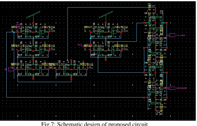
Schematic design of proposed circuit
IJEDR1504129
International Journal of Engineering Development and Research (www.ijedr.org)747
Fig.7: Schematic design of proposed circuit
VI. SIMULATION AND RESULTS
A bit full adder circuit based on double gate MOSFET technique is proposed. Simulation of the propose circuit is done by using the Cadence virtuoso tools. It is used for measurement of power consumption, leakage, and delay of circuit at 45nm technology with different supply voltage. The simulations have been done for different supply voltage and temperature. The proposed circuit is simulated for voltage range of 0.3 to 0.7 at room temperature.
Fig 8: Input and Output waveform for proposed circuit
The table I show power dissipation of proposed circuit for given range of supply voltage which is from 0.3 to 0.7 V. This table shows that circuit can perfectly for low power. The delay for given circuit is 10 nsec. This table also reveals that this circuit work for wide range of supply voltage. The table II shows variation power with temperature and this table tells that power dissipation is increased with increasing temperature. This is due to affects like phonon scattering at high temperatures.
Table 1: Power dissipation Serial
no
Power supply(mV)
Power dissipation
(𝑛𝑊)
Power delay product(×e18)
1 300 6.1 61
2 400 9.8 98
3 500 17.0 170
4 600 28.0 280
IJEDR1504129
International Journal of Engineering Development and Research (www.ijedr.org)748
Table 2: Variation power with temperatureDELAY
Propagation delay is the required by a digital signal to travel from that input of the circuit to the output. The propagation delay is related to the speed of the architecture as inversely in nature and hence it is important performance parameter. The basic equation of delay in presence of sleep
transistor is shown in Eq. below
𝑑𝑠𝑙𝑒𝑒𝑝=
𝐾.𝐶𝑙.𝑉𝑑𝑑 𝑉𝑑𝑑−2 𝑉𝑥−𝑉𝑡𝑙2
(4)
Where, 𝑉𝑋 is the potential of the virtual rails, and K is the proportionality constant, CL is the load capacitance at the gate output; VtL is the low-voltage threshold. Fig.9. Delay Comparison Graph for different technology
Fig9: Delay comparison graph for different technology
VII. CONCLUSION
In this paper we designed the double gate full adder with Power Gating technique. Double Gate MOSFET technology achieves low leakage and high performance operation with high speed. The Power Gating technique reduces the leakage current in standby mode. Different parameters are analysed at various voltage supplies. The active power is reduced by 64% and delay is reduced by 14% respectively as compared to conventional double gate full adder. Simulation results of double gate full adder have been performed on cadence virtuoso with 45nm technology.
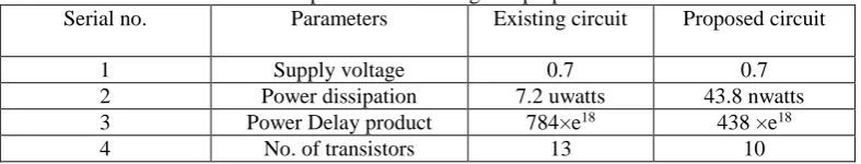
Table 3: Comparison for existing and proposed circuit
Serial no. Parameters Existing circuit Proposed circuit
1 Supply voltage 0.7 0.7
2 Power dissipation 7.2 uwatts 43.8 nwatts
3 Power Delay product 784×e18 438 ×e18
4 No. of transistors 13 10
The table 3 shows a comparison for existing and proposed circuit. The table III shows a comparison between exiting and proposed. This table shows that 98% power reduction in proposed circuit. The overall power delay product is reduces by 46%. Although the delay is increased but still PDP is low as compare to base paper. Again there is lower number of transistors are used the proposed circuit has 10 transistors whereas the existing circuit has 13 transistors. The proposed circuit shows overall improvement for designing full adder circuit.
VIII. ACKNOWLEDGMENT
The authors would have been grateful to KUK University to provide cadence software lab and valuable support by its staff. Serial no. Temperature(degrees) PDP
(×e18)
1 0 47
2 10 49
3 20 55
4 30 65
5 40 76
IJEDR1504129
International Journal of Engineering Development and Research (www.ijedr.org)749
REFERENCES
[1] Sun, X.-G., Mao, Z.-G., and Lai F.-C. “A 64 bit parallel CMOS adder for high performance processor ”, Proc. IEEE Asia-Pacific Conf. on ASIC, 2002, pp. 205–208.
[2] VahidMoalemi and Ali Afzali -Kusha, “Subthreshold 1-bit Full adder cellsin sub-100nm technologies”, IEEE Computer Society Annual Symposium on VLSI (ISVLSI-07, Porto Alegre, Brazil, March, 2007.
[3] N. H. E. Weste and D. Harris, "CMOS VLSI Design: A Circuit andSystems Perspective," Third Edition," Addison Wesley, 2005.
[4] AP. Chandrakasan, S.Sheng, and .W.Brodersen , "Low-Power CMOSdigital design," IEEE 1. Solid-State Circuit, vol. 27, pp. 473-483, Apr.1992.
[5] 1.B Kuo and 1.-H. Lou, "Low-Voltage CMOS VLSI Circuit," JohnWiley & Sons, Inc.,1999.
[6] S.M. kang, and L.Yusuf, "CMOS Digital integrated Circuit Analysis andDesign," McGraw-Hili, 1999.
[7] M. Zhang, 1. Gu, and C. H. Chang, "A novel hybrid pass logic withstatic CMOS output drive full-adder cell," Proc. 36th IEEE IntSymp. Circuits and Systems, vol. Y, Bangkok, Thailand, May 2003, pp. 317-320.
[8] C. K. Tung, Y. C. Hung, S. H. Shieh, and G. S. Huang, "A Low- PowerHigh-Speed Hybrid CMOS Full Adder for Embedded System," Designand Diagnostics of Electronic Circuits and Systems IEEE, April 2007,Page(s): 1-4.
[9] F. Jiang, Z. G. Mao, W. F. He, Q. Wang, "A new full adder design fortree structured arithmetic circuits," Proc. 2nd IntConf on (ICCET2010), voL4, pp.Y4-246-V4-249, 16-18 April, 2010.
[10] J. Wang, S. Fang, and W. Feng, “New efficient designs for XOR and XNOR functions on the transistor level”, IEEE J. Solid-State Circuits, vol. 29, no. 7,Jul. 1994, pp. 780–786.
[11] R. Shalem, E. John, and L. K. John, “A Novel Low Power Energy Recovery Full Adder Cell” in Proc. IEEE Great Lakes VLSI Symp., pp. 380–383, Feb.1999.
[12] H. T. Bui, A. K. Al-Sheraidah and Y. Wang, “Design and Analysis of 10-transistor Full Adders using Novel XOR-XNOR Gates” , Proceedings of ICSP2000.
[13] P. M. Lee, C. H. Hsu, and Y. H. Hung, “Novel 10-T full adders realized by GDI structure” IEEE International Symposium on Integrated Circuits (ISIC-2007).
[14] J. F. Lin, Y. T. Hwang, M. H. Sheu and C. C. Ho, “A novel High-Speed and Energy Efficient 10-Transistor Full Adder Design”, IEEE Transactions onCircuits and System—I: Regular Papers, VOL. 54, NO. 5, May 2007.
[15] D. Radhakrishnan, “Low-voltage low-power CMOS full adder,” in Proc. IEEE Circuits Devices Systems, vol. 148, FEB 2001, pp 19-24.