R E S E A R C H
Open Access
Verify level control criteria for multi-level
cell flash memories and their applications
Yongjune Kim
1, Jaehong Kim
2, Jun Jin Kong
2, B V K Vijaya Kumar
1*and Xin Li
1Abstract
InM-bit/cell multi-level cell (MLC) flash memories, it is more difficult to guarantee the reliability of data asMincreases. The reason is that anM-bit/cell MLC has 2Mstates whereas a single-level cell (SLC) has only two states. Hence, compared to SLC, the margin of MLC is reduced, thereby making it sensitive to a number of degradation mechanisms such as cell-to-cell interference and charge leakage. In flash memories, distances between 2Mstates can be controlled by adjusting verify levels during incremental step pulse programming (ISPP). For high data reliability, the control of verify levels in ISPP is important because the bit error rate (BER) will be affected significantly by verify levels. AsM increases, the verify level control will be more important and complex. In this article, we investigate two verify level control criteria for MLC flash memories. The first criterion is to minimize the overall BER and the second criterion is to make page BERs equal. The choice between these criteria relates to flash memory architecture, bits per cell, reliability, and speed performance. Considering these factors, we will discuss the strategy of verify level control in the hybrid solid state drives (SSD) which are composed of flash memories with different number of bits per cell.
Introduction
Flash memory is now the fastest growing memory seg-ment, driven by the rapid growth of mobile devices and solid state drives (SSD). To satisfy the market demand for lower cost per bit and higher density of nonvolatile memory, there are two approaches: (1) technology scaling, (2) multi-level cell (MLC) [1-4].
As the technology continues to scale down, flash mem-ories suffer from more severe physical degradation mech-anisms such as cell-to-cell interference (coupling) and charge leakage [5,6]. In addition, M-bit/cell MLC flash memories have 2M states within the threshold voltage window whereas the single-level cell (SLC) has only two states. Therefore, the reliability of stored data is an impor-tant challenge for high density flash memories.
In order to cope with this reliability problem, many approaches have been proposed. The incremental step pulse programming (ISPP), which is the most widely used programming scheme, was proposed to maintain a tight cell threshold voltage distribution for high reliability [7,8].
*Correspondence: [email protected]
1Electrical and Computer Engineering, Carnegie Mellon University, Pittsburgh, PA, 15213, USA
Full list of author information is available at the end of the article
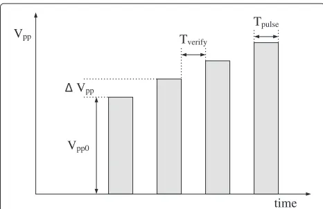
ISPP is a program and verify strategy with a stair case pro-gram voltageVppas illustrated in Figure 1, whereVppis
the incremental step size. During each program and ver-ify cycle, the floating gate threshold voltage is first boosted by up toVppand then compared with the
correspond-ing verify level. If the threshold voltage of the memory cell is still lower than the verify level, the program and ver-ify iteration continues. Otherwise, further programming of this cell is disabled [7-10].
Therefore, positions of program states (except the erase state) are determined by verify levels and the tightness of each program state depends on the incremental step size Vpp. By reducingVpp, the cell threshold voltage
dis-tribution can be made tighter, but the programming time will increase [7,8]. In brief, ISPP can control both the dis-tances between states by verify levels and the tightness of program states by the incremental step size.
For SLC, determining the verify level of the program-ming state is a simple problem because there is only one program state and the margin between the erase state and the program state is sufficiently large so that small changes in the margin will not change the error rates noticeably. However, the verify level control issue forM-bit/cell flash memories is more important and complex than that for SLC. This is because 2Mstates have to be crammed within
Vpp0 Vpp
Tpulse Tverify
time Vpp
Figure 1Program pulses in ISPP.A verify operation is carried out after each pulse.Vppis the incremental step size of the program pulse.Vpp0is the initial value of the program pulse.Tverifyis the verify read time.Tpulseis the program pulse width [10].
the given constrained threshold voltage windowW. More states will significantly reduce the margin between states and bit error rates (BER) will vary in response to small changes in verify levels. Furthermore, the number of verify levels which ISPP has to control increases from 1 (for SLC) to 2M−1 (forM-bit/cell MLC). In addition, as explained in the following, the multipage architecture of MLC flash memories makes verify level control more complex than SLC.
Most MLC flash memories adopt the multipage tecture. The important property of the multipage archi-tecture is that different bits of a single cell are assigned into different pages [10-15]. Therefore, BERs of each page can be different. As a page is the unit of data that is pro-grammed and read at one time, the error control coding (ECC) should be applied within the same page. It means that each page is composed of one or several codewords. Therefore, ECC has to be designed for the worst page BER and this leads to wasted redundancy for the other (i.e., bet-ter) pages. This uneven page BER problem is an important and practical issue and there have been several attempts to deal with it [11-15].
To deal with this different page BERs issue, we investi-gate two verify level control criteria for MLC flash mem-ories. The first criterion is to minimize the overall BER. The second criterion is to make all page BERs equal [14]. These two criteria will be formulated as convex optimiza-tion problems. After solving these optimizaoptimiza-tion problems, we will compare the numerical results from two criteria. In addition, the advantages and disadvantages of the two criteria will be discussed based on reliability, speed per-formance, and architecture of MLC flash memories. To the best of authors’ knowledge, the convex optimization approach for verify levels of ISPP has not been addressed in the open literature though experimental approaches could be investigated in industry.
An interesting way to combine the speed advantage of SLC and the cost advantage of MLC is to use a hybrid solid state drive (SSD) that judiciously uses both SLC and MLC flash memories. The basic idea of hybrid SSD is to complement the drawbacks of SLC and MLC with each other’s advantages [16-19]. Based on the architecture of the hybrid SSD and properties of the proposed ver-ify level control criteria, we propose a strategy to apply the proper verify level control criterion for the hybrid SSD. This strategy is aimed at both reliability and speed performance.
The rest of this article is organized as follows: Section “Cell threshold voltage distribution” discusses the cell threshold voltage distribution under the assumption of a Gaussian mixture model (GMM). Based on this statisti-cal model, the overall BER and the page BER are derived. Sections “Criteria for verify level control” and “ECC and flash memories of multipage architecture” address ver-ify level control criteria and discuss their advantages and disadvantages for various MLCs (M = 2 ∼ 4) consider-ing multipage architecture and ECC. Section “Hybrid SSD and strategy for verify level control” proposes a method to choose these criteria for the hybrid SSD based on reliabil-ity and speed performance. Finally, Section “Conclusion” concludes this article.
Cell threshold voltage distribution
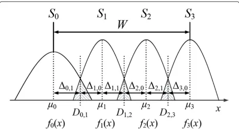
InM-bit/cell flash memory, the cell threshold voltage dis-tribution is composed of 2M states from S0 (the erase state) to S2M−1 (the highest state). Even though there
are tail cells and asymmetry in cell distributions, the cell threshold voltage distribution of flash memories could be approximated as a sum of Gaussian distributions [6,20,21]. Therefore, we will model the cell threshold voltage distri-butionf(x)by the following GMM.
f(x)=
2M−1
i=0
P(Si)fi(x)
= 1
2M
2M−1
i=0 1
√
2π σi
exp
−(x−μi)2 2σi2
(1)
where x refers to the threshold voltage and fi(x) is a
Gaussian pdf with meanμiand standard deviationσi cor-responding to the stateSi. P(Si)is the probability of the
stateSi. If data size is sufficiently large and a scrambler is
used, then we can assume thatP(S0)≈ · · · ≈P(S2M−1)≈
1
2M with high probability.
dis-Figure 2Cell threshold voltage distribution for 2-bit/cell flash memories.There are four states fromS0toS3. Each stateSican be modeled by the distributionfi.
tance between the mean of the erase state and the mean of the highest state, which is given by
W =μ2M−1−μ0. (2)
The overall BER (i.e., BERoverall) is the total number of erroneous bits divided by the total number of data bits which contains data of all pages. If the Gray mapping is used, there is only one bit difference between Si and Si+1. For example, in 2-bit/cell MLC, states S0, S1, S2, andS3denote bit patterns 11, 10, 00, and 01. Probabili-ties that cells are misread as states which are more than two states away from the original state are much smaller than probabilities of cells being misread as adjacent states and thus are negligible. Therefore, the overall BER can be expressed as
BERoverall= 1
M2M
2M−2
i=0
Q
i,1
σi,1
+Q
i+1,0
σi+1,0
(3)
where i,1 is the distance from μi to Di,i+1 and i+1,0 is the distance fromμi+1 toDi,i+1.Di,i+1is the optimal decision level between Si and Si+1, which satisfies the condition offi(Di,i+1) = fi+1(Di,i+1)[22-24]. In addition,
σi,0andσi,1are used separately for convenience although σi,0 = σi,1 = σi. The tail probability function Q(x) is defined as
Q(x)=
∞
x
1
√
2π exp
−t2
2
dt. (4)
If we change the index ofi,j intok andσi,jintoρk by k=2i+j, (3) can be rewritten as
BERoverall= 1
M2M
22M−1
k=1
Q k ρk (5)
where allks are positive since it is natural thatμi+1> μi.
Most MLC flash memories adopt multipage architec-tures [10]. In this multipage architecture, ECC encoding
and decoding are performed within each page. This means that pages with higher BERs will suffer from worse decod-ing failure rate. Therefore, the BER of each page could be more important than the overall BER in terms of ECC [11,13-15].
The page BER (i.e., the BER of each page) depends on the mapping scheme that converts a state level to cor-responding bit representation. We will define BERpagem
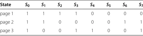
as the BER of pagem. For example, if the 2-bit/cell flash memory adopts the Gray mapping of Table 1, the data of page 1 are obtained by one read operation betweenS1and
S2. Therefore, the BER of page 1 is determined byf1(x)and
f2(x). In order to read the data of page 2, two read opera-tions (one betweenS0andS1, and another betweenS2and
S3) are required. Then the BER of page 2 is determined by
f0(x)andf1(x),f2(x), andf3(x). Therefore, page BERs for 2-bit/cell are given by
BERpage 1= 1 4 Q 1,1 σ1,1 +Q 2,0 σ2,0 ,
BERpage 2= 1 4 Q 0,1 σ0,1 +Q 1,0 σ1,0 +Q 2,1 σ2,1 +Q 3,0 σ3,0 . (6)
By the same method, page BERs for 3-bit/cell adopting the Gray mapping of Table 2 are given by
BERpage 1= 1 8 Q 3,1 σ3,1 +Q 4,0 σ4,0 ,
BERpage 2= 1 8 Q 1,1 σ1,1 +Q 2,0 σ2,0 +Q 5,1 σ5,1 +Q 6,0 σ6,0 ,
BERpage 3= 1 8 Q 0,1 σ0,1 +Q 1,0 σ1,0 +Q 2,1 σ2,1 +Q 3,0 σ3,0 +Q 4,1 σ4,1 +Q 5,0 σ5,0 +Q 6,1 σ6,1 +Q 7,0 σ7,0 . (7)
Similarly, page BERs for 4-bit/cell or more could be derived from the mapping scheme provided.
Table 1 Gray mapping for 2-bit/cell flash memories
State S0 S1 S2 S3
page 1 1 1 0 0
Table 2 Gray mapping for 3-bit/cell flash memories
State S0 S1 S2 S3 S4 S5 S6 S7
page 1 1 1 1 1 0 0 0 0
page 2 1 1 0 0 0 0 1 1
page 3 1 0 0 1 1 0 0 1
The overall BER of (3) can be expressed as the mean of page BERs, which is given by
BERoverall= 1
M M
m=1
BERpagem. (8)
The distance between the means ofSiandSi+1isμi+1−
μi=i,1+i+1,0. We will termμi+1−μias the distance
fromSito Si+1, and the distance fromSi toSi+1will be determined byi,1andi+1,0. For all states, we will define two parameters as follows.
−
→ =
1,. . .,2(2M−1)
(9)
− →ρ =ρ
1,. . .,ρ2(2M−1)
(10)
wherek = i,jandρk = σi,jbyk = 2i+j. Therefore, −
→
and−→ρ will represent the all distances between states and the tightness of program states, respectively, and they will determine the overall BER and the page BERs. In the ISPP scheme,−→can be controlled by verify levels and−→ρ by the incremental step size. In the following section, we will propose criteria for verify level control, which means how to determine−→ at the given−→ρ.
Criteria for verify level control
We investigate two verify level control criteria. The first criterion is to minimize the overall BER, which is aimed at only reliability. The second criterion is to make page BERs equal considering both the reliability and the multipage architecture. These two criteria will be formulated as opti-mization problems. If the parameters ofW(=μ2M−1−μ0)
and−→ρ are given,−→ =
1,. . .,2(2M−1)
will be the variables of optimization problems.
We will show that the proposed criteria for verify level control are convex optimization problems. Therefore, the (globally) optimal solution can be efficiently found using numerical optimization techniques and the interior-point method was used to obtain the numerical results [25]. Also, mathematical conditions for the optimal solutions of these criteria are derived.
Criterion 1: minimize overall BER
The first criterion is to minimize the overall BER. This cri-terion 1 forM-bit/cell flash memories can be formulated as follows.
minimize−→
g1 −→ =
22M−1
k=1
Q k ρk subject to
22M−1
k=1
k=W
k ≥0, k=1,. . ., 22M−1
(11)
whereg1
−→
=M2M·BERoverallby (5).
The cost functiong1(·)is a nonnegative weighted sum ofQ(·). From (4), the second derivative ofQ(·)is given by
d2Q(x)
dx2 =
x √
2πexp
−x2
2
≥0 forx≥0. (12)
Sincekis the distance andρkis the standard deviation,
all ks and ρks are always positive. Therefore, (11) is a convexoptimization problem and can be solved by several numerical methods [25].
We will define the LagrangianG1as follows.
G1(−→,λ,−→η )=g1+λ
⎛ ⎝2(2
M−1)
k=0
k−W ⎞ ⎠+2(2
M−1)
k=1
ηk(−k)
(13)
where −→η =
η1,. . .,η2(2M−1)
. The optimal solution of (11) has to satisfy the following Karush-Kuhn-Tucker (KKT) conditions [25].
ηk ≥0, k=1,. . ., 22M−1
ηk(−k)=0, k=1,. . ., 22M−1
∇G1=0
(14)
Since all ks are positive, ηk = 0 for all k by (14), which results from complementary slackness. Therefore, the optimal solution will satisfy the following condition from (13) and (14).
∂G1
∂k = − 1
√
2π ρkexp
−2k
2ρk2
+λ=0,
k=1,. . ., 22M−1.
(15)
From (15), the optimal solution has to satisfy the fol-lowing condition in order to minimize the overall BER.
f0μ0+0,1=f1μ1−1,0= · · ·
=f2M−1
μ2M−1−2M−1,0
=λ (16)
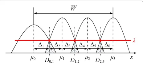
Figure 3 illustrates the condition of (16) for minimiz-ing the overall BER. In addition, Figure 3 shows that the decision level Di,i+1 satisfies the condition fi
Di,i+1
Figure 3Example of criterion 1 for 2-bit/cell.This example illustrates the condition which minimizes the overall BER.
fi+1
Di,i+1
which corresponds to the definition of the optimal decision level [22-24].
If variances for all states are equal (i.e.,σk2 = σ2), then allks become = 2 W
(2M−1) from (11) and (15). In this
case, the BER of pagem(1≤m≤M)is given by
BERpagem=
1 2M−m ·Q
σ
. (17)
(17) shows that BERpagem+1will be twice BERpagemif
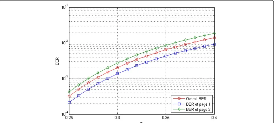
vari-ances for all states are same. WhenM = 2, BERpage 1= 1
2·Q
σ
and BERpage 2=Q
σ
. From (8), BERoverall=34·
Qσ. Figure 4 shows BERpage 1, BERpage 2, and BERoverall as a function ofσfor 2-bit/cell flash memories. From (17), it is seen that the ratio of page BERs for 3-bit/cell is 1:2:4. For 4-bit/cell flash memories, the ratio of page BERs will be 1:2:4:8 [11-15]. Therefore, using criterion 1 makes the difference between page BERs larger asMincreases.
In addition, the difference between page BERs from cri-terion 1 could increase if variances for states are not equal. For example, it is possible that the erase state S0 has wider distribution than other program states since the cell threshold voltage distribution of the erase state is not con-trolled as tightly as other program states by ISPP [8]. In this case, more errors will occur betweenS0andS1, which results in the increase of the last page BER (BERpageM)
in the Gray mapping schemes of Tables 1 ∼ 3. Table 4 shows the increase of the difference between page BERs. In Table 4, we assumed that the standard deviation of the erase state(S0)isσ0and standard deviations of other pro-gram states(S1 ∼ S3) are same asσ. As the erase state distribution becomes broader, criterion 1 will lead to more difference between page BERs.
Criterion 2: make page BERs equal
The second criterion is to make the page BERs equal [14]. In addition, the overall BER has to be made as small as possible. Therefore, this criterion 2 for M-bit/cell flash memories can be formulated as follows.
minimize−→
,ε
g2=ε
subject to
22M−1
k=1
k =W
hm
−→
≤ε, m=1,. . .,M
k ≥0, k=1,. . ., 22M−1
(18)
where hm
−→
= 2M· BERpagem. Therefore, from the
constraints of this optimization problem,εwill represent the maximum value among all page BERs. While trying to minimizeε, we can find the optimal solution which min-imizes the overall BER among candidates satisfying the following condition.
BERpage 1≈BERpage 2≈ · · · ≈BERpageM≈BERoverall
≈ ε
2M
(19)
In other words, even though the formulation in (18) does not explicitly set the page BERs to be identical, it implicitly minimizes the difference between all page BERs. Intu-itively, if BERpagem is higher than other page BERs, the
optimization in (18) will try to reduce BERpagemand make
it as close to other page BERs as possible.
(18) is aconvexoptimization problem sincehm
−→
is a nonnegative weighted sum of convex functionQ(·). The convex property of Q(·) was shown in (12). Therefore, the optimal solution can be obtained by several numerical methods.
The LagrangianG2associated with (18) is given by
G2(−→,−→λ,−→η )=g2+λ0·
k−W
+ M
m=1
λm(hm−ε)
+
2(2M−1)
k=1
ηk(−k)
(20)
Table 3 Gray mapping for 4-bit/cell flash memories
State S0 S1 S2 S3 S4 S5 S6 S7 S8 S9 S10 S11 S12 S13 S14 S15
page 1 1 1 1 1 1 1 1 1 0 0 0 0 0 0 0 0
page 2 1 1 1 1 0 0 0 0 0 0 0 0 1 1 1 1
page 3 1 1 0 0 0 0 1 1 1 1 0 0 0 0 1 1
Figure 4BER of 2-bit/cell flash memories using Criterion 1.The constrained voltage windowWis assumed to be 5.
where−→λ =
λ0,. . .,λ2(2M−1)
and−→η =
η1,. . .,η2(2M−1)
. The optimal solution of (18) has to satisfy the following KKT conditions.
λm≥0, m=1,. . .,M
λm(hm−ε)=0, m=1,. . .,M
ηk≥0, k=1,. . ., 22M−1
ηk(−k)=0, k=1,. . ., 22M−1
∇G2=0
(21)
As discussed in criterion 1, all ηks will be zero due to
complementary slacknessof (21).
Figure 5 shows how criterion 2 works for 2-bit/cell flash memories. In order to make page BERs equal,|μ2−μ1| = 3+4of criterion 2 has to be reduced compared to that of criterion 1. Meanwhile,|μ1−μ0| =1+2and|μ3−
μ2| =5+6will be larger than those of criterion 1.
Table 4 BERpage 2/BERpage 1for 2-bit/cell flash memories
(W=5)
σ σ0=σ σ0=2σ σ0=3σ σ0=4σ
0.20 2.00 2.55 3.16 3.83
0.22 2.00 2.56 3.19 3.89
0.24 2.00 2.57 3.22 3.97
0.26 2.00 2.58 3.26 4.04
0.28 2.00 2.59 3.30 4.12
0.30 2.00 2.61 3.34 4.21
From (21), we can obtain following conditions for the optimal solution of 2-bit/cell flash memories.
∂G2
∂ε =1−λ1−λ2=0, ∂G2
∂i =
λ0+λ1·√ 1 2π ρiexp
−2i
2ρi2
=0, i=3, 4,
∂G2
∂j =
λ0+λ2· 1
√
2π ρj
exp
−
2
j
2ρj2
=0, j=1, 2, 5, 6
(22)
If one ofλms (form = 0,. . .,M) is zero, then allλms
should be zero since ∂G2
∂k =0 and
1
√
2π ρk exp
−2k
2ρk2
>0
for allk. However, if allλms are zero, the condition of 1− λ1−λ2=0 in (22) cannot hold. Therefore, we can see that λm = 0, which results inhm−ε= 0 by KKT conditions
of (21). It means that all page BERs will be equal for the optimal solution of (18)∵hm
−→
=2M·BER
pagem
. Taking into account the aforementioned discussions, the conditions of (22) can be modified by
λ1+λ2=1,
1
√
2π ρi
exp
−2i
2ρi2
= −λ0
λ1
, i=3, 4,
1
√
2π ρj
exp
−
2
j
2ρj2
= −λ0
λ2, j=1, 2, 5, 6
(23)
which are illustrated in Figure 5.
Figure 6 shows the numerical results of criterion 2 for 2-bit/cell flash memories when variances for all states are equal toσ. All page BERs and the overall BER are made equal by criterion 2. Even if variances for all states are not equal, the optimal solution can be obtained by the same method.
It is worth mentioning that the overall BER from crite-rion 2 is worse than that from critecrite-rion 1. The reason is that the overall BER increases when we try to make page BERs equal. Figure 7 shows the degradation of the overall BER from criterion 2 compared to criterion 1 for 2-bit/cell flash memories. In order to measure this degradation, we will define the degradation ratioγ given by
γ = BERoverallfrom criterion 2 BERoverallfrom criterion 1
. (24)
Figure 8 shows the degradation ratioγ for 2-bit/cell, 3-bit/cell and 4-3-bit/cell flash memories where we assume
that variances for all states are same. For 2-bit/cell,γ is about 1.05, which means that the degradation of the over-all BER is 5 %. Meanwhile, the degradation of 3-bit/cell is about 14 %(γ ≈1.14)and the degradation of 4-bit/cell is about 25 %(γ ≈1.25). These results reveal that equalizing page BERs causes an increase of the overall BER.
Verify level control criteria and charge leakage
After programming data into flash memories, the cell threshold voltage distribution can change because of charge leakage. The cell threshold voltage distribution change due to charge leakage can be modeled as a change in the mean and the variance of the distributions, i.e., [6]
μpost=μpre+μshift,
σpost2 =σpre2 +σshift2 , (25)
whereμpreandσpre2 are the mean and the variance before charge leakage.μpostandσpost2 are the mean and the vari-ance after charge leakage.μshiftandσshift2 are the mean and the variance of threshold voltage shift by charge leakage. μshift andσshift2 depend on the program and erase (P/E) cycle count, retention time and temperature [6].
The proposed verify level control criteria should be applied based onμpostandσ2postbecauseμpostandσpost2 will determine the BER of flash memories. Therefore, we have to controlμpre andσpre2 considering the amount of
μshiftandσshift2 . Basically,μpreandσpre2 can be controlled by verify levels and the incremental step sizeVppof ISPP
though physical mechanisms such as cell-to-cell inter-ference, program disturbance, and background pattern dependency also affectμpreandσpre2 [5,7,8].
Figure 7Comparison between the overall BER from the two criteria.The constrained voltage windowWis assumed to be 5.
Via chip testing, we can measure the amount of μshift and σshift2 as a function of P/E cycle count and reten-tion time [6]. However, the allowable maximum values of μshift andσshift2 are generally used because ECC has to be designed to guarantee the reliability even in the worst case, which is also called end-of-life (EOL). EOL assumes the allowable maximum P/E cycle count and the allow-able maximum retention time. Therefore, it is a practical method to apply the proposed verify level control criteria based onμpost andσpost2 of EOL. In this case,μpost and
σpost2 should be used to formulate the convex optimization problems shown in (11) and (18). Other than this minor modification, no additional change is required for our proposed mathematical formulations.
Verify level control criteria and other statistical distributions
We will extend these proposed verify level control criteria for other distributions. Suppose that the threshold volt-age distribution of each stateSican be approximated as an
arbitrary distributionφi(x) which has a maximum value
atx= νi (i.e.,νiis the mode ofφi(x)). Instead of (2), the
constrained voltage windowW will be defined by
W =ν2M−1−ν0. (26)
The distance betweenSiandSi+1will be defined asνi+1−
νi instead ofμi+1−μi and it is assumed thatνi+1 > νi
for alli. In the case of Gaussian distributions,μiandνiare
same.
Then, the error probability between Si and Si+1 (i.e.,
Ei,i+1) is given by
Ei,i+1=P(Si)· ∞
νi+i,1
φi(t)dt+P(Si+1)·
νi+1−i+1,0
−∞ φi+1(t)dt
(27)
whereP(Si)is the probability ofSi. In addition,i,1is the distance fromνitoDi,i+1andi+1,0is the distance from
νi+1toDi,i+1.Di,i+1is the decision level betweenSi and Si+1.
Sinceνi and νi+1 of (27) are also variables which are determined by−→ =
1,. . .,2(2M−1)
, we will modify (27) as follows.
Ei,i+1=P(Si)· ∞
ν0+i,1
φi,−(t)dt+P(Si+1)·
ν2M−1−i+1,0
−∞ φi+1,+(t)dt
(28)
where φi,−(t) = φi(t+(νi−ν0)) and φi+1,+(t) = φi+1
t−ν2M−1−νi+1
.ν0andν2M−1are fixed value by
(26).
The overall BER and the page BERs ofM-bit/cell MLC flash memories are nonnegative weighted sums ofEi,i+1 fori=0,. . ., 2M−2. Therefore, ifEi,i+1is a convex func-tion ofi,1 andi+1,0, the proposed verify level control criteria will be convex optimization problems.
The Hessian matrix ofEi,i+1is given by
Ifφi,−(ν0+i,1)=φi(νi+i,1)≤0 andφi+1,+(ν2M−1− i+1,0) = φi+1(νi+1−i+1,0) ≥ 0 (i.e.,∇2Ei,i+1is pos-itive semidefinite),Ei,i+1is aconvexfunction. Therefore, the conditions ofφi(x)for convex optimization problems
are given by
φ0(x)≤0 forx> ν0,
φi(x)≥0 forx< νi and φi(x)≤0 forx> νi,
i=1,. . ., 2M−2 φ2M−1(x)≥0 forx< ν2M−1,
(30)
which mean thatφi(x)should be aunimodaldistribution for convex optimization.
Since the measured threshold voltage distributions of recent flash memory products [2-4] are unimodal, the proposed verify level control criteria can be effectively applied to flash memories. In addition, the proposed ver-ify level control criteria can be applied to other memo-ries such as phase change memory (PCM) because the measured distributions of PCM in literature seem to be unimodal [26-28]. Especially, [26] claims that the distribu-tions of PCM could be approximated by the log-normal distribution in spite of the anomalous tail. Therefore, our proposed verify level control criteria are expected to be useful in PCM.
ECC and flash memories of multipage architecture When algebraic ECC such as Bose, Chaudhuri, and Hoc-quenghem (BCH) codes are used in a binary symmetric channel (BSC) with bit error probabilityp, the word error rate (WER) is given by
WER(p)≤
n
i=t+1
n
i
pi(1−p)n−i (31)
where n is the codeword length and t is the error cor-recting capability. The bound becomes an equality when the decoder corrects all combinations of errors up to and includingterrors, but no combinations of errors greater
∇2E
i,i+1=
⎡ ⎢ ⎢ ⎢ ⎣
∂2Ei,i+1 ∂2i,1
∂2Ei,i+1 ∂i,1∂i+1,0
∂2Ei,i+1 ∂i+1,0∂i,1
∂2Ei,i+1 ∂2i+1,0
⎤ ⎥ ⎥ ⎥ ⎦
=
⎡ ⎢ ⎢ ⎣
−P(Si)·
dφi,−(ν0+i,1)
di,1
0
0 −P(Si+1)·
dφi+1,+(ν2M−1−i+1,0)
di+1,0
⎤ ⎥ ⎥ ⎦
=
−P(Si)·φi,−(ν0+i,1) 0
0 P(Si+1)·φi+1,+(ν2M−1−i+1,0)
.
than t (i.e., bounded distance decoder) [29,30]. In this article, the bounded distance decoder will be considered. Once ECC parameters such as nandtare selected, the WER is a function of onlyp.
Though errors in flash memories are generally not sym-metric, the asymmetric component of errors could be minimized if the decision level are selected appropriately [22-24]. For example, for 2-bit/cell flash memories, the errors of page 1 will be symmetric if we select the deci-sion levelD1,2betweenS1andS2which makesQ
1,1
σ1,1
= Q
2,0
σ2,0
in (6). Similarly, the errors of page 2 can be
sym-metric if we choose the decision levelsD0,1andD2,3which makeQ
0,1 σ0,1
= Q
1,0
σ1,0
andQ
2,1 σ2,1
= Q
3,0 σ3,0
in (6).
In the case of σi = σi+1, the decision level Di,i+1 which makes the errors symmetric is equal to the optimal decision levelDi,i+1as follows.
Di,i+1=Di,i+1= 1
2(μi+μi+1) (32)
Although σi = σi+1, if σi is not substantially differ-ent fromσi+1, the difference betweenDi,i+1andDi,i+1is almost negligible [22]. Therefore, the BER based onDi,i+1 is similar to that based onDi,i+1. Considering these, we will use (31) to calculate the WER of flash memories [31]. In most of flash memories, program and read operations are performed in page units [10]. Therefore, ECC encod-ing and decodencod-ing are also performed in page units [13-15]. It means that the WER of each page depends on each page BER which corresponds topin (31). Therefore, the overall
WER is given by
WERoverall= 1
M M
m=1
WERBERpagem
(33)
where WERBERpagem
is the WER of pagem.
Theorem 1.If0<=p<= n−t1, then WER(p)of (31) is a convex function of p.
Proof. WER(p) of (31) can be computed from the incomplete beta functionIx(a,b)[32].
WER(p)=Ip(t+1,n−t)
=(n−t)
n t
p
0
xt(1−x)n−t−1dx
The second derivative of WER(p)is given by
d2WER(p)
dp2 =(n−t)
n
t
pt−1(1−p)n−t−2{t−p(n−1)}.
Therefore,d2WERdp2(p) >=0 when 0<=p<= n−t1. Generally, the operation range of ECC satisfies the con-dition of 0 <= p <= n−t1. By the convex property of WER(p)and (33), the following equation holds.
WER
1
M M
m=1
BERpagem
≤ 1
M M
m=1
WERBERpagem
(34)
Figure 10Comparison between the overall WER from criterion1 and from criterion 2 for 2-bit/cell, 3-bit/cell and 4-bit/cell.The BCH code (n=8752,k=8192,t=40) is applied. The constrained voltage windowWis assumed to be 5.
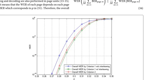
(34) reveals that the overall WER would be improved by interleaving. If the interleaver is applied for the whole data from page 1 to page M, all page BERs will be averaged into the overall BER of (8) and the overall WER would be improved according to (34). In other words, minimizing the overall BER (i.e., criterion 1) is preferred over achiev-ing identical page BERs (i.e., criterion 2), if interleavachiev-ing is applied.
Actually, the application of interleaving and similar ideas have been proposed in order to resolve the uneven page BER problem and improve the reliability [11,12]. However, the adoption of interleaving will slow down the program and read speed performance because the inter-leaver should wait to collect at leastMpages data before program and read operation in the multipage architec-ture. Especially, random speed performance would be more degraded than sequential speed performance when employing an interleaver (see Section “Hybrid SSD and strategy for verify level control”).
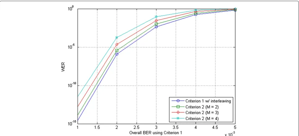
Therefore, criterion 2 could be a practical alternative for flash memories because it does not degrade the speed performance and exhibits only slight degradation of the overall BER as shown in Figure 8. In addition, criterion 2 does not require large memory buffer for interleaving. Figure 9 shows that the overall WER from criterion 2 is much better than that of criterion 1 without interleav-ing and only slightly worse than that of criterion 1 with interleaving for 2-bit/cell flash memories.
However, the WER degradation of criterion 2 will increase asMincreases as shown in Figure 10. The rea-son is that the overall BER from criterion 2 will be much
worse than that from criterion 1 for largeMas shown in Figure 8. Therefore, criterion 2 would not be appropriate for largeMin terms of the reliability.
Hybrid SSD and strategy for verify level control In order to reduce the cost of SSD and maintain the speed performance and the durability, the hybrid SSD has been proposed [16,17]. The basic idea is to use both SLC flash memories and MLC (usually 2-bit/cell) flash memories. The SLC flash memory has an edge over the MLC flash memory in terms of the speed performance and the dura-bility. However, the MLC flash memory is cheaper than the SLC flash memory. Therefore, combining them can allow both types of flash memories to complement each other [16-19].
Hot / Cold
Detection Module SLC Hot Data
Write
MLC Garbage Collection Cold Data
Write Write
Read
Recently, many flash translation layer (FTL) mapping schemes classify incoming data intohot andcold based on the access frequency and size. If a data is updated frequently, it is referred to as hot, and otherwise cold. Generally, small data are accessed more often, and they are classified as hot data. Meanwhile, cold data correspond to bulk writes at low frequencies [16,18]. The speed perfor-mance of SSD is classified into random speed perforperfor-mance and sequential speed performance. The random speed performance is measured in input/output operations per second (IOPS) and the sequential speed performance is measured by transfer rate or throughput such as MB/sec [33]. Considering the characteristics of hot and cold data, we see that the random speed performance is a pivotal fac-tor for hot data and the sequential speed performance is important for cold data.
Figure 11 illustrates the architecture of the hybrid SSD. In this architecture, the hot and cold detection module separates hot data from cold ones dynamically and directs them either to SLC or MLC based on the decision. Before SLC flash memories run out of free blocks, the hybrid SSD performs garbage collection to merge valid cold data of SLC and move them into MLC [18].
Based on this architecture of the hybrid SSD, we pro-pose that criterion 1 with interleaving is suitable for stor-ing cold data in MLC because the interleavstor-ing would have only a small impact on the sequential speed performance for the cold data access and the garbage collection. Of course, we do not need to consider the verify level control criterion for SLC.
In addition, we can anticipate a lower cost and high den-sity hybrid SSD which combines two types of MLC flash memories. For example, 2-bit/cell may replace SLC and 4-bit/cell may be used in place of 2-bit/cell. Unlike the conventional hybrid SSD which combines SLC and MLC of 2-bit/cell, we have to consider the verify level control criterion for both hot and cold data. We propose that criterion 2 will be appropriate for 2-bit/cell flash memo-ries which mainly deal with hot data. For 4-bit/cell which usually stores cold data, criterion 1 with interleaving will be suitable considering the sequential speed performance and the reliability.
Conclusion
In this article, we investigated the verify level control criteria of ISPP for MLC flash memories. These criteria are formulated and solved by convex optimization. Crite-rion 1 can minimize the overall BER, however it requires interleaving in multipage architecture which reduces the speed performance. Criterion 2 is suitable for multipage architecture especially for 2-bit/cell flash memories. The problem of criterion 2 is that the error rate degradation will increase for more bits per cell.
Based on these advantages and disadvantages of verify level criteria, we investigated the application of verify level control criteria for the hybrid SSD. By selecting the proper criterion considering the architecture of the hybrid SSD, we can achieve both reliability and speed performance.
The verify level control criteria and the proposed for-mulation of optimization problems can be extended to other emerging memories such as PCM which are mod-eled by unimodal distributions.
Competing interests
The authors declare that they have no competing interests.
Author details
1Electrical and Computer Engineering, Carnegie Mellon University, Pittsburgh,
PA, 15213, USA.2Samsung Electronics Co., Ltd., Hwasung, Gyeonggi-do, 445-701, Korea.
Received: 14 April 2012 Accepted: 17 August 2012 Published: 5 September 2012
References
1. K Prall, inIEEE 22nd Non-Volatile Semiconductor Memory WorkshopScaling non-volatile memory below 30nm, pp. 5–10 (2007)
2. K-T Park, O Kwon, S Yoon, M-H Choi, I-M Kim, B-G Kim, M-S Kim, Y-H Choi, S-H Shin, Y Song, J-Y Park, J-E Lee, C-G Eun, H-C Lee, H-C Kim, J-H Lee, J-Y Kim, T-M Kweon, H-J Yoon, T Kim, D-K Shim, J Sel, J-Y Shin, P Kwak, J-M Han, K-S Kim, S Lee, Y-H Lim, T-S Jung, inISSCC Dig. Tech PapersA 7MB/s 64Gb 3-bit/cell DDR NAND flash memory in 20nm-node technology, pp. 212–213 (2011)
3. S-D T Kim, J Lee, H Park, B Cho, K You, J Baek, C Lee, M Yang, M Yun, J Kim, E Kim, H Jang, S Chung, B-S Lim, Y-H Han, A Koh, inISSCC Dig. Tech Papers
32Gb MLC NAND flash memory with Vth margin-expanding schemes in 26nm CMOS, pp. 202–204 (2011)
4. C Trinh, N Shibata, T Nakano, M Ogawa, J Sato, Y Takeyama, K Isobe, B Le, F Moogat, N Mokhlesi, K Kozakai, P Hong, T Kamei, K Iwasa, J Nakai, T Shimizu, M Honma, S Sakai, T Kawaai, S Hoshi, J Yuh, C Hsu, T Tseng, J Li, J Hu, M Liu, S Khalid, J Chen, M Watanabe, H Lin, et al., inISSCC Dig. Tech. PapersA 5.6MB/s 64Gb 4b/cell, NAND flash memory in 43nm CMOS, pp. 245–246 (2009)
5. J-D Lee, S-H Hur, J-D Choi, Effects of floating-gate interference on NAND flash memory cell operation. IEEE Electron. Device Lett.23(5), 264–266 (2002)
6. N Mielke, H Belgal, I Kalastirsky, P Kalavade, A Kurtz, Q Meng, N Righos, J Wu, Flash EEPROM threshold instabilities due to charge trapping during program/erase cycling. IEEE Trans. Device Mater. Reliab.
4(3), 335–344 (2004)
7. K-D Suh, B-H Suh, Y-H Lim, J-K Kim, Y-J Choi, Y-N Koh, S-S Lee, S-C Kwon, B-S Choi, J-S Yum, J-H Choi, J-R Kim, H-K Lim, A 3.3 V 32 Mb NAND flash memory with incremental step pulse programming scheme. IEEE J. Solid-State Circ.30(11), 1149–1156 (1995)
8. T-S Jung, Y-J Choi, K-D Suh, B-H Suh, J-K Kim, Y-H Lim, Y-N Koh, J-W Park, K-J Lee, J-H Park, K-T Park, J-R Kim, J-H Lee, H-K Lim, A 117-mm23.3-V only 128-Mb multilevel NAND flash memory for mass storage applications. IEEE J. Solid-State Circ.31(11), 1575–1583 (1996)
9. G Dong, N Xie, T Zhang, On the use of soft-decision error-correction codes in NAND flash memory. IEEE Trans. Circ. Syst. I.58(2), 429–439 (2011) 10. K Takeuchi, T Tanaka, T Tanzawa, A multipage cell architecture for
high-speed programming multilevel NAND flash memories. IEEE J. Solid-State Circ.33, 1228–1238 (1998)
11. M Murrin, U.S. patent 7, 493, 457 (2009)
12. S Litsyn, I Alrod, E Sharon, M Murin, M Lasser, U.S. patent 7, 681, 109 (2010) 13. M Lasser, U.S. patent 8, 055, 972 (2011)
14. SC Park, H Eun, S-H Song, JJ Kong, DH Chae, U.S. patent 7, 983, 082 (2011) 15. G Dong, N Xie, T Zhang, inIEEE Globecom Workshop on Application of
embracing intra-cell unbalanced bit error characteristics in MLC NAND flash memory, pp. 1915–1920 (2010)
16. L-P Chang, A hybrid approach to NAND-flash-based solid-state disks. IEEE Trans. Comput.59(10), 1337–1349 (2010)
17. L-P Chang, inAsia and South Pacific Design Automation Conference (ASPDAC)Hybrid solid-state disks: Combining heterogeneous NAND flash in large SSDs, pp 428–433 (2008)
18. S Jung, J Kim, Song Y, in46th annual Design Automation Conference (DAC)
Hierarchical architecture of flash-based storage systems for high performance and durability, pp. 907–910 (2009)
19. N Duann, SLC and MLC hybrid.Flash Memory Summit(2008)
20. DL Kencke, R Richart, S Garg, SK Banerjee, A multilevel approach toward quadrupling the density of flash memory. IEEE Electron. Device Lett. 19, 86–88 (1998)
21. J Wang, T Courtade, H Shankar, RD Wesel, inIEEE Global Communications ConferenceSoft information for LDPC decoding in flash:
mutual-information optimized quantization, pp. 5–9 (2011) 22. GP Agrawal,Fiber-Optic Communication Systems,3rd edn. (Wiley, New
York, 2002)
23. YJ Kim, JH Kim, JJ Kong, HR Son, SH Song, U.S. patent application, publication no 2010/0296350 (2010)
24. H Zhou, A Jiang, J Bruck, inIEEE Int. Symposium on Information Theory (ISIT)
Error-correcting schemes with dynamic thresholds in nonvolatile memories, 2109–2113 (2011)
25. S Boyd, L Vandenberghe,Convex Optimization(Cambridge University Press, Cambridge, 2004)
26. D Mantegazza, D Ielmini, A Pirovano, B Gleixner, AL Lacaita, E Varesi, F Pellizzer, R Bez, inIEEE International Electron Devices Meeting (IEDM)
Electrical characterization of anomalous cells in phase change memory arrays, pp. 1–4 (2006)
27. F Bedeschi, R Fackenthal, C Resta, EM Donze, M Jagasivamani, EC Buda, F Pellizzer, DW Chow, A Cabrini, GMA Calvi, R Faravelli, A Fantini, G Torelli, D Mills, R Gastaldi, G Casagrande, A bipolar-selected phase change memory featuring multi-level cell stroage. IEEE J. Solid-State Circ.
44(1), 217–227 (2009)
28. G Servalli, inIEEE International Electron Devices Meeting (IEDM)A 45nm generation phase change memory technology, pp. 1–4 (2009) 29. S Lin, DJ Costello Jr.,Error Control Coding: Fundamentals and Applications,
2nd edn. (Pearson Prentice-Hall, Upper Saddle River, 2004)
30. B Sklar,Digital Communications Fundamentals and Applications,2nd edn. (Pearson Prentice-Hall, Upper Saddle River, 2001)
31. N Mielke, T Wu, J Kessenich, H Schares, E Trivedi, F Goodness, E Nevill, R Leland, inIEEE International Reliability Physics Symposium (IRPS)Bit error rate in NAND flash memories, pp. 9–19 (2008)
32. WH Press, BP Flannery, SA Teukolsky, WT Vetterling,Numerical Recipes,3rd edn. (Cambridge University Press, New York, 2007)
33. D Narayanan, E Thereska, A Donnelly, S Elnikety, A Rowstron, in4th ACM European Conference on Computer Systems (EuroSys)Migrating enterprise storage to SSDs: analysis of tradeoffs, 145–158 (2009)
doi:10.1186/1687-6180-2012-196
Cite this article as:Kimet al.:Verify level control criteria for multi-level
cell flash memories and their applications.EURASIP Journal on Advances in
Signal Processing20122012:196.
Submit your manuscript to a
journal and benefi t from:
7Convenient online submission 7Rigorous peer review
7Immediate publication on acceptance 7Open access: articles freely available online 7High visibility within the fi eld
7Retaining the copyright to your article