22
REDUCTION OF EFFECT OF TIMING JITTER ON
HIGH SPEED OFDM SYSTEM USING OVER
SAMPLING TECHNIQUE
Unnava Divya
1Koteswarararao Seelam
2 1,2ECE Department 1M.Tech student , 2Associate Professor
SMCE,Tummalapalem [email protected]
ABSTRACT
Orthogonal frequency division multiplexing (OFDM) is used in many wireless broadband communication systems because it is a simple and scalable solution to intersymbol interference caused by a multipath channel. Very recently the use of OFDM in optical systems has attracted increasing interest. Data rates in optical fiber systems are typically much higher than in RF wireless systems.The impairments caused by timing jitter are a significant limiting factor in the performance of very high data rate OFDM systems. In this letter we show that oversampling can reduce the noise caused by timing jitter. Both fractional oversampling achieved by leaving some band-edge OFDMsubcarriers unused and integral oversampling are considered. The theoretical results are compared with simulation results for the case of white timing jitter showing very close agreement. Oversampling results in a 3 dB reduction in jitter noise power for every doubling of the sampling rate.OFDM is a multicarrier modulation scheme that provides strong robustness against intersymbol interference (ISI) by dividing the broadband channel into many narrowband sub- channels in such a way that attenuation across each sub channel stays flat. Orthogonalization of sub channels is performed with low complexity by using the fast Fourier transform (FFT). The serial high-rate data stream is converted into multiple parallel low-rate streams, each modulated on a different subcarrier.
1. INTRODUCTION
ORTHOGONAL frequency division multiplexing (OFDM) is used in many wireless broadband communication systems because it is a simple and scalable solution to intersymbol interference caused by a multipath channel. Very recently the use of OFDM in optical systems has attracted increasing interest.
Data rates in optical fiber systems are typically much higher than in RF wireless systems. At these very high data rates, timing jitter is emerging as an important limitation to the performance of OFDM systems. A major source of jitter is the sampling clock in the very high speed analog-to-digital converters (ADCs) which are required in these systems. Timing jitter is also emerging as a problem in high frequency bandpass sampling OFDM radios. The effect of timing jitter has been analyzed in . These project focuses on the coloured low pass timing jitter which is typical of systems using phase lock loops (PLL). They consider only integral oversampling. In OFDM, fractional oversampling can be achieved by leaving some band-edge subcarriers unused. In this letter we investigate both fractional and integral oversampling. We extend the timing jitter matrix proposed in to analyze the detail of the intercarrier interference (ICI) in an oversampled system. Very high speed ADCs typically uses a parallel pipeline architecture not a PLL and for these the white jitter which is the focus of this project is a more appropriate model[1]
1.1OFDM (Orthogonal Frequency Division Multiplexing):
23
OFDM depends on Orthogonality principle. Orthogonality means, it allows the sub carriers, which are orthogonal to each other, meaning that cross talk between co-channels is eliminated and inter-carrier guard bands are not required. This greatly simplifies the design of both the transmitter and receiver, unlike conventional FDM;a separate filter for each sub channel is not required. Orthogonal Frequency Division Multiplexing (OFDM) is a digital multi carrier modulation scheme, which uses a large number of closely spaced orthogonal sub-carriers. A single stream of data is split into parallel streams each of which is coded and modulated on to a subcarrier, a term commonly used in OFDM systems. Each sub-carrier is modulated with a conventional modulation scheme (such as quadrature amplitude modulation) at a low symbol rate, maintaining data rates similar to conventional single carrier modulation schemes in the same bandwidth. Thus the high bit rates seen before on a single carrier is reduced to lower bit rates on the subcarrier. In practice, OFDM signals are generated and detected using the Fast Fourier Transform algorithm. OFDM has developed into a popular scheme for wideband digital communication, wireless as well as copper wires.Actually, FDM systems have been common for many decades. However, in FDM, the carriers are all independent of each other. There is a guard period in between them and no overlap whatsoever. This works well because in FDM system each carrier carries data meant for a different user or application. FM radio is an FDM system. FDM systems are not ideal for what we want for wideband systems. Using FDM would waste too much bandwidth. This is where OFDM makes sense[2,3]
2
2.. RREELLAATTEEDD WWOORRKK
2
2..11OOFFDDMMggeenneerraattiioonn::
To generate OFDM successfully the relationship between all the carriers must be carefully controlled to maintain the orthogonality of the carriers. For this reason, OFDM is generated by firstly choosing the spectrum required, based on the input data, and modulation scheme used. Each carrier to be produced is assigned some data to transmit. The required amplitude and phase of the carrier is then calculated based on the modulation scheme (typically differential BPSK, QPSK, or QAM).
24
Fig. 2.2 OFDM Block Diagram
Fig. 2.2 shows the setup for a basic OFDM transmitter and receiver. The signal generated is a base band, thus the signal is filtered, then stepped up in frequency before transmitting the signal. OFDM time domain waveforms are chosen such that mutual orthogonality is ensured even though sub-carrier spectra may overlap. Typically QAM or Differential Quadrature Phase Shift Keying (DQPSK) modulation schemes are applied to the individual sub carriers. To prevent ISI, the individual blocks are separated by guard intervals wherein the blocks are periodically extended.
2
2..22FFFFTT&&IIFFFFTT::
In practice, OFDM systems are implemented using a combination of FFT and IFFT blocks that are mathematically equivalent versions of the DFT and IDFT, respectively, but more efficient to implement.An OFDM system treats the source symbols (e.g., the QPSK or QAM symbols that would be present in a single carrier system) at the Tx as though they are in the freq-domain. These sym’s are used as the i/p’s to an IFFT block that brings the sig into the time domain. The IFFT takes in N sym’s at a time where N is the num of sub carriers in the system. Each of these N i/p sym’s has a symbol period of T secs. Recall that the basis functions for an IFFT are N orthogonal sinusoids. These sinusoids each have a different freq and the lowest freq is DC. Each i/p symbol acts like a complex weight for the corresponding sinusoidal basis fun. Since the i/p sym’s are complex, the value of the sym determines both the amplitude and phase of the sinusoid for that sub carrier.The IFFT o/p is the summation of all N sinusoids. Thus, the IFFT block provides a simple way to modulate data onto N orthogonal sub carriers. The block of N o/p samples from the IFFT make up a single OFDM sym. The length of the OFDM symbol is NT where T is the IFFT i/p symbol[6] period mentioned above.
2.3 FFT & IFFT DIAGRAM
After some additional processing, the time-domain sig that results from the IFFT is transmitted across the channel. At the Rx, an FFT block is used to process the received signal and bring it into the freq domain. Ideally, the FFT o/p will be the original sym’s that were sent to the IFFT at the Tx. When plotted in the complex plane, the FFT o/p samples will form a constellation, such as 16-QAM. However, there is no notion of a constellation for the time-domain sig. When plotted on the complex plane, the time-domain sig forms a scatter plot with no regular shape. Thus, any Rx processing that uses the concept of a constellation (such as symbol slicing) must occur in the frequency- domain.
3.SYSTEM MODEL:
3.1 Idealized system model
25
3.1.1 Transmitter
An OFDM carrier signal is the sum of a number of orthogonal sub-carriers, with baseband data on each sub-carrier being independently modulated commonly using some type of quadrature amplitude modulation (QAM) or phase-shift keying (PSK). This composite baseband signal is typically used to modulate a main RF carrier. is a serial stream of binary digits. By inverse multiplexing, these are first demultiplexed into parallel streams, and each one mapped to a (possibly complex) symbol stream using some modulation constellation (QAM, PSK, etc.). Note that the constellations may be different, so some streams may carry a higher bit-rate than others.An inverse FFT is computed on each set of symbols, giving a set of complex time-domain samples. These samples are then quadrature-mixed to pass band in the standard way. The real and imaginary components are first converted to the analogue domain using digital-to-analogue converters (DACs); the analogue signals are then used to modulate cosine and sine waves at the carrier frequency, , respectively. These signals are then summed to give the transmission signal, .[9]
3.1.2 Receiver
26
This returns parallel streams, each of which is converted to a binary stream using an appropriate symbol detector. These streams are then re-combined into a serial stream, , which is an estimate of the original binary stream at the transmitter.
3.2 Mathematical description
If sub-carriers are used, and each sub-carrier is modulated using alternative symbols, the OFDM symbol alphabet consists of combined symbols.
The low-pass equivalent OFDM signal is expressed as:
where are the data symbols, is the number of sub-carriers, and is the OFDM symbol time. The sub-carrier spacing of
makes them orthogonal over each symbol period; this property is expressed as:
where denotes the complex conjugate operator and is the Kronecker delta.
To avoid intersymbol interference in multipath fading channels, a guard interval of length is inserted prior to the OFDM block. During this interval, a cyclic prefix is transmitted such that the signal in the interval equals the signal in the interval . The OFDM signal with cyclic prefix is thus:
The low-pass signal above can be either real or complex-valued. Real-valued low-pass equivalent signals are typically transmitted at baseband wire line applications such as DSL use this approach. For wireless applications, the low-pass signal is typically complex-valued; in which case, the transmitted signal is up-converted to a carrier frequency . In general, the transmitted signal can be represented as:
3.3 Principles of OFDM
27
--- (1)
where is the frequency of the th subcarrier. One baseband OFDM symbol (without a cyclic prefix) multiplexes modulated subcarriers:
...(2)
where is the th complex data symbol (typically taken from a PSK or QAM symbol constellation) and is the length of
the OFDM symbol. The subcarrier frequencies are equally spaced
---(3)
which makes the subcarriers on orthogonal. The signal (2) separates data symbols in frequency by overlapping subcarriers, thus using the available spectrum in an efficient way. The left half of Figure 1 illustrates the quadrature component of some of the subcarriers of an OFDM symbol. The right half of Figure 1 illustrates how the subcarriers are packed in the frequency domain.
Figure 2 shows time and frequency characteristics of an OFDM signal with 1024 subcarriers. As the OFDM signal is the sum of a large number of independent, identically distributed components its amplitude distribution becomes approximately Gaussian due to the central limit theorem. Therefore, it suffers from large peak-to-average power ratios. In addition, OFDM symbols of the form (2) can have large band power as illustrated in Figure 2. Large peak-to-average power ratios also cause out-of-band emission because of amplifier non-linearities. Section 3 discusses ways to deal with high peak-to-average power ratios and out-of-band power.
The OFDM symbol (2) could typically be received using a bank of matched filters. However, an alternative demodulation is used in practice. T-spaced sampling of the in-phase and quadrature components of the OFDM symbol yields (ignoring channel impairments such as additive noise or dispersion)
, ... (4)
which is the inverse discrete Fourier transform (IDFT) of the constellation symbols . Accordingly, the sampled data is demodulated with a DFT. This is one of the key properties of OFDM, first proposed by Weinstein and Ebert, [1971]. The DFT, typically implemented with an FFT, actually realizes a sampled matched-filter receiver in systems without a cyclic prefix.
28
In signal processing, oversampling is the process of sampling a signal with a sampling frequency significantly higher than twice the bandwidth or highest frequency of the signal being sampled. Oversampling helps avoid aliasing, improves resolution and reduces noise
3.4.1 Oversampling factor
An oversampled signal is said to be oversampled by a factor of β, defined as
---(5)
Or .
where
fs is the sampling frequency
• B is the bandwidth or highest frequency of the signal; the Nyquist rate is 2B.
3.4.2 Motivation
There are three main reasons for performing oversampling:
Anti-aliasing
It aids in anti-aliasing because realizable analog anti-aliasing filters are very difficult to implement with the sharp cutoff necessary to maximize use of the available bandwidth without exceeding the Nyquist limit. By increasing the bandwidth of the sampled signal, the anti-aliasing filter has less complexity and can be made less expensively by relaxing the requirements of the filter at the cost of a faster sampler. Once sampled, the signal can be digitally filtered and downsampled to the desired sampling frequency. In modern integrated circuit technology, digital filters are much easier to implement than comparable analog filters of high order[10]
3.4.3 Resolution
In practice, oversampling is implemented in order to achieve cheaper higher-resolution A/D and D/A conversion. For instance, to implement a 24-bit converter, it is sufficient to use a 20-bit converter that can run at 256 times the target sampling rate. Averaging a group of 256 consecutive 20-bit samples adds 4 bits to the resolution of the average, producing a single sample with 24-bit resolution. Number of samples required to get n bits of additional data:
samples = 22n ----(6)
The result in software from n samples is then divided by 2n:
29
Note that this averaging is possible only if the signal contains perfect equally distributed noise (i.e. if the A/D is perfect and the signal's deviation from an A/D result step lies below the threshold, the conversion result will be as inaccurate as if it had been measured by the low-resolution core A/D and the oversampling benefits will not take effect)[11]
3.4.4 Noise
If multiple samples are taken of the same quantity with a different (and uncorrelated) random noise added to each sample, then averaging N samples reduces the noise variance (or noise power) by a factor of 1/N. See standard error (statistics). This means that the signal-to-noise-ratio improves by a factor of 4 (6 dB or one additional meaningful bit) if we oversample by a factor of 4 relative to the Nyquist rate (i.e. a β of 4) and low-pass filter. Certain kinds of A/D converters known as delta-sigma converters produce disproportionately more quantization noise in the upper portion of their output spectrum. By running these converters at some multiple of the target sampling rate, and low-pass filtering the oversampled down to half the target sampling rate, it is possible to obtain a result with less noise than the average over the entire band of the converter. Delta-sigma converters use a technique called noise shaping to move the quantization noise to the higher frequencies.
3.4.5 Timing Jitter
In any system that uses voltage transitions to represent timing information, jitter is an unfortunate part of the equation. In essence, jitter is the deviation of timing edges from their intended locations. Historically, jitter was kept under control by system designers by using relatively low signaling rates. But the timing margins associated with modern high-speed serial communication buses renders such strategies moot. As signaling rates climb above 2 GHz and corresponding voltage swings continue to shrink, a given system’s timing jitter becomes a significant portion of the signaling interval and, hence, a baseline performance limiter. A simple and intuitive definition for jitter is part of the SONET specification: “Jitter is defined as the short-term variations of a digital signal’s significant instants from their ideal position in time.” This definition requires thumbnail descriptions of its components. Just what is meant by “short-term?” Timing variations are, by convention, split into two categories: jitter and wander. Timing variations that occur slowly are known as wander; jitter refers to variations that occur more rapidly. The threshold between wander and jitter is defined by the International Telecommunication Union (ITU) as 10 Hz. Wander is generally not an issue in serial communication links, where a clock-recovery circuit eliminates it. And that odd term “significant instants” refers to the transitions, or edges, between logic states in the digital signal. Significant instants are the exact moments when the transitioning signal crosses a chosen amplitude threshold, known variously as the reference level or decision threshold. Finally, the term “ideal position” can be thought of in this way.
3. SYSTEM MODEL AND TIMING JITTER MATRIX
30
Fig 4.1 OFDM block diagram
4.2 Definition of timing jitter
N complex values representing the constellation points are used to modulate up to N subcarriers. Timing jitter can be introduced at a number of points in a practical OFDM system but in this letter we consider only jitter introduced at the sampler block of the receiver ADC. Fig. shows how timing jitter is defined.
Ideally the received OFDM signal is sampled at uniform intervals of T/N. The dashed lines in Fig. represent uniform sampling intervals. The solid arrows represent the actual sampling times. The effect of timing jitter is to cause deviation between the
actual sampling times and the uniform sampling intervals. Fig. shows the discrete timing jitter for this example. In OFDM systems while timing jitter degrades system performance, a constant time offset from the ‘ideal’ sampling instants is automatically corrected without penalty by the equalizer in the receiver.In we showed that the effect of timing jitter can be described by a timing jitter matrix. The compact matrix form for OFDM systems with timing jitter is
---(8)
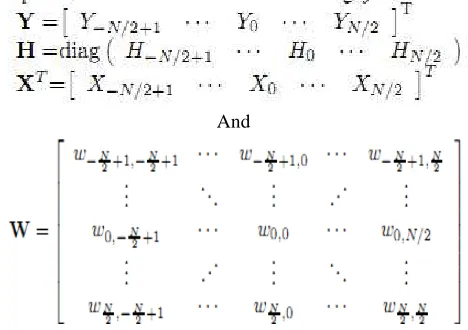
where X, Y and N are the transmitted, received and additive white Gaussian noise (AWGN) vectors respectively, H is the channel response matrix and W is the timing jitter matrix
where
And
Timing jitter causes an added noise like component in the received signal.
----(9)
31
---(10)
where n is the time index, k is the index of the transmitted subcarrier and l is the index of the received subcarrier 4.1 Advantages:
1.To analyze the detail of the intercarrier interference (ICI) in an oversampled system. 2.Very high speed ADCs typically use a parallel pipeline architecture.
3.Oversampling can reduce the degradation caused by timing jitter in OFDM systems. 4.A linear reduction in jitter noise power as a function of oversampling rate
4.2 Dis advantages:
1.High frequency subcarriers cause more ICI than lower frequency subcarriers, but that the resulting ICI is spread equally across all subcarriers.
5. RESULTS &DISCUSSION
-300 -200 -100 0 100 200 300
10 12 14 16 18 20 22 24
Subcarrier index
P
o
w
e
r
in
(
d
B
)
Nv=600 Nv=512 Nv=492 Nv=472 Nv=452 Nv=400
32
1 2 3 4 5 6 7 8 9 10
-16 -14 -12 -10 -8 -6 -4
Over sampling factor
A
v
e
re
a
g
e
j
it
te
r
N
o
is
e
i
n
d
B
Simulation Theoritical
33
0 5 10 15 20 25 30 35 40
10-4 10-3 10-2 10-1 100
Performance Analysis
SNR
(dB)---B
it
E
rr
o
r
R
a
te
(
d
B
)-
[image:12.595.205.408.118.433.2]
---)
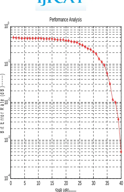
Fig 5.3 Bit Error Rate verses SNR(dB)
6.CONCLUSIONS
It has been shown both theoretically and by simulation that oversampling can reduce the degradation caused by timing jitter in OFDM systems. Two methods of oversampling were used: fractional oversampling achieved by leaving some of the band-edge subcarriers unused, and integral oversampling implemented by increasing the sampling rate at the receiver. For the case of white timing jitter both techniques result in a linear reduction in jitter noise power as a function of oversampling rate. Thus oversampling gives a 3 dB reduction in jitter noise power for every doubling of sampling rate. It was also shown that in the presence of timing jitter, high frequency subcarriers cause more ICI than lower frequency subcarriers, but that the resulting ICI is spread equally across all subcarriers.
7. REFERENCES
[1] J. Armstrong, “OFDM for optical communications,” J. Light wave Technol.,vol. 27, no. 1, pp. 189-204, Feb. 2009.
[2] V. Syrjala and M. Valkama, “Jitter mitigation in high-frequency band pass sampling OFDM radios,” in Proc. WCNC 2009, pp. 1-6.
34
[4] U. Onunkwo, Y. Li, and A. Swami, “Effect of timing jitter on OFDM based UWB systems,” IEEE J. Sel. Areas Commun., vol. 24, pp. 787-793,2006.
[5] L. Yang, P. Fitzpatrick, and J. Armstrong, “The Effect of timing jitter on high-speed OFDM systems,” in Proc. AusCTW 2009, pp. 12-16. [6] L. Sumanen, M. Waltari, and K. A. I. Halonen, “A 10-bit 200-MS/s CMOS parallel pipeline A/D converter,” IEEE J. Solid-State Circuits, vol. 36, pp. 1048-55, 2001.
[6] L. Sumanen, M. Waltari, and K. A. I. Halonen, “A 10-bit 200-MS/s CMOS parallel pipeline A/D converter,” IEEE J.
Solid-State Circuits, vol. 36, pp. 1048-55, 2001
[7] G. Einarsson, “Address assignment for a time-frequency, coded, spread spectrum system," Bell Syst. Tech. J., vol. 59, no. 7, pp. 1241-1255, Sep. 1980.
[8] S. B. Wicker and V. K. Bhargava (eds.), Reed-Solomon Codes and Their Applications. Wiley-IEEE Press, 1999.
[9] G.-C. Yang and W. C. Kwong, Prime Codes with Applications to CDMA Optical and Wireless Networks. Norwood, MA: Artech House, 2002.
[10] C.-Y. Chang, C.-C. Wang, G.-C. Yang, M.-F. Lin, Y.-S. Liu, and W. C. Kwong, “Frequency-hopping CDMA wireless communication systems using prime codes," in Proc. IEEE 63rd Veh. Technol. Conf., pp. 1753- 1757, May 2006.