ISSN 2348 – 7968
Silicon Photonics: A Review
Mr. Akshaykumar S. Hedaoo1, Prof. Atul N. Shire2 and Prof. Atul P. Shingade3
1
Department of Electronics And Telecommunication, JDIET, Yavatmal, (M.S.) - 445001, India
2
Department of Electronics And Telecommunication, JDIET, Yavatmal, (M.S.) - 445001, India
3
Department of Electronics And Telecommunication, JDIET, Yavatmal, (M.S.) - 445001, India
Abstract
Silicon photonics is the future of optical transmission. As researchers are more interested to replace copper wire with the optical technology. They are using photons instead of electron to carry out the transmission with in the silicon photonics chips. Due to photons the speed of data transfer will increase as compared to wired configuration. This paper reviews the growth of silicon photonics compared to last few years and a promising future of photonics. By taking advantage of silicon photonics, new products can scale bandwidth availability to meet the future demand.
Keywords: Silicon, Modulators, Mach-Zehnder, SiGe, Detectors, Lasers, Avalanche Photodetector
1. Introduction
Taking in mind silicon as the core material the new technology of producing optical devices and circuits has been introduce. Using standard CMOS fabrication process integration of optical and electronic components on single chip can be done. At mid wave Si or SiGe/Si components perform well, long wave and very long –wave infrared (THz) ranges. For optical communication the transparency at wavelengths (1270 nm to 1625 nm) and its intrinsic band gap of silicon (1.1 eV) typically favors and manipulates the light. Computers in present using copper wires to connect different peripherals which actually degrades the signal strength and constraints it to the maximum length.
Fig. 1 Basic block diagram of optical link
ISSN 2348 – 7968
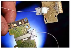
Fig. 2 50 Gbps silicon photonics transmit module
Figure above shows the 50gbps optical link module developed by Intel group. Firstly silicon chip provide laser light which travels through optical fibre and reaches to another silicon chip where it convert laser data in to electrical signals. Due to Optoelectronic systems integration on silicon on substrate (SOI) realizable with complementary metal-oxide semiconductor technology, allows large scale manufacturing and low cost for Si photonic device. Still the work is going on the development of integration methods of low loss waveguides, high quality resonators, high speed modulators and optically pumped lasers on silicon chip for effective photonic circuits with low cost and power consumption.
2. Literature Review
In 1958, Jack Kibly from Texas instrument demonstrated that it was possible to fabricate a resistor, capacitor, and transistor using single-crystal silicon[2]. Which led to first truly integrated circuit and was awarded by Nobel prize in year 2000. Due to which microelectronics industry witnessed a miraculous reduction in individual device size, and hence increases in chip functionality in five decades. And the trend has been set up that approximately after every 24 months world has witnessed the doubling of device density.
In 1962 Gordon Moore predicted Moore’s law which remained pertinent to the present day, forming the motivation for the International Technology Roadmap for Semiconductors (ITRS) in 1993.
In 1980, using the design and manufacturing principles from microelectronics industries, taking in mind silicon as the base material for fabrication of photonics circuit researchers began to develop their projects and research. Silicon material proved to be an ideal material for planar light wave circuit (PLC) fabrication. Silicon is virtually transparent to wavelengths > 1100 nm, on the other hand silicon dioxide (SiO2) shares its chemical composition with glass fiber, providing a degree of interference with long-haul, fiber-optic technology. Silicon has a relatively
high refractive index around 3.5 which leads to the fabrication of waveguides on the nanometer scale. Due to the size and nature of indirect bandgap, which prevents the deviating formation of efficient optical sources, and detectors compatible with subbandgap wavelengths which leads to limitation of silicon in photonics area[3][4]. A bit previous in the year 2000, primary correspondence for integrated silicon photonics was introduce in telecommunications, so-called first-generation. But due to the development of relatively large waveguide which were used in fiber optic network and optical switching has dominated silicon photonics. But in the late 1990’s telecom industry has seen the abundance of technology touted as the favored tribune for integrated photonic circuit fabrication. At that time, Bookham Technology of the UK reached high level of competency in silicon photonics and showed that the methods used in the microelectronics industry to fabricate large volumes of devices in a economical manner could be applied to photonic circuits. Due to increase in engineers and scientists dedication to silicon photonic device design in the 1990s led directly to vast development in the field of silicon photonics in telecom sector.
Second-generation silicon photonics started in February 2004, led by Mario Paniccia and his group at Intel Corp. proclaim the demonstration of an optical device, fabricated wholly in silicon[5]. The potential for integration of photonic and electronic functionality as a method for reducing the excessive power dissipation in microelectronic circuits was thus demonstrated. The year 2004 also saw the publication of the first textbooks to deal with the subject of silicon photonics[6][7]. In the relatively short period, the field has expanded rapidly. Waveguide dimensions are now measured in square nanometers rather than square microns, and demonstration of modulation speeds in excess of 20 GHz have been done[8].
3. High-Speed Silicon Modulator
ISSN 2348 – 7968
Fig. 3 Modulation process of wave
in the above fig (3) shows the modulation process of two wavelength. Here we can see that if two sine wave are completely matched then they are added and the output is twice the amplitude of individual waves. And if they are totally unmatched then they cancle each other out. Free carrier plasma dispersion effect is come through by silicon integration circuits modulation. Various constraints such as narrow waveguide, bandwidth, low power consumption, modulation efficiency is kept in mind while integrating optical modulators on silicon substrate.
Table 1: Comparison of silicon modulators.
There are different types of modulators, Table 1 lists some of the important parameters for each specific modulator. The ring modulator is compact and operating at sub-voltage, but the optical and modulation bandwidth are both limited. It is suitable for high density and narrow bandwidth applications. In opposite, the Electro absorption Modulator (EAM) has slightly larger footprint, fair modulation efficiency and high modulation bandwidth up to 16 GHz. To meet large optical bandwidth reconfigurable communication system must be require for that EAM is a good candidate. The Mach-Zehnder Modulator (MZM) has a larger footprint and requires higher bias condition; however, it has a wider optical bandwidth, higher large signal modulation, and potential applications such as switches and routers make it very inhibiting for future all optical communication networks.
4. Metal-Oxide Semiconductor (Mos)
Capacitor-Based Silicon Modulator
Fig. 4 Cross-section view of the MOS capacitor-based on silicon optical modulator.
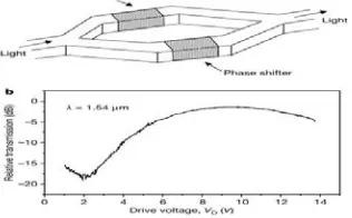
Modulation can be achieved by driving MOS capacitor in accumulation mode in this type of modulator. When Positive voltage VD applied on the gate, it forms depletion and inversion layer across the waveguide region. Large amount of silicon charge carriers accumulate in the depletion region due to which there is change in the refractive index. It occurs mainly due to the positive charge. Due to Change in refractive index there will also be the changes in the phase shift and attenuation in one or both arms of interferometer.
Fig. 5 (a) Phase shifter in both arms of MZI, (b) Drive voltage change with relative transmission
ISSN 2348 – 7968
dielectric width. Intel in 2004 made it’s own MOS capacitor, with modulation bandwidth exceeding 1GHz.
5. Electro-Absorption Modulators
Electro absorption modulator is a type of semiconductor device that modulates the intensity of laser beam via electric voltage. Main principle of operation is based on the Franz–Keldysh effect. Absorption type modulators have high operating speed, low power dissipation and low operating voltage as compared to plasma dispersion-based modulators. Modulation bandwidth of 10 GHz can be achieved through these modulators. Electroabsorption modulators find their applications in high speed modulation, high extinction ratio, low drive voltage and integrability.
6. Hybrid Silicon Modulator
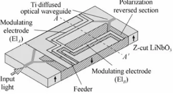
High speed operation, large bandwidth and good modulation efficiency are the main requirement of an efficient modulator. MZI based modulator has the bandwidth near to 100nm while electro-absorption modulators are less than 30nm. Due to requirement of high speed operation, hybrid silicon modulators are developed, where the III-V material epitaxial layer appear on silicon-on-insulator (SOI) wafer by wafer bonding techniques. LiNbO3 is the most widely used material as electro-optic modulators. Electro-optic coefficient is high and mature fabrication technology making it suitable for modulation applications. Earlier, LiNbO3 modulators have modulation speed of 20Gbps but now ultrafast LiNbO3 of 60Gbps have been developed by titanium (Ti) diffusing.
Fig. 6 LiNbO3 modulator with Ti diffusing
Feeder provides the input signal with same phases and amplitude which is further divided in to two signals on the modulating electrodes E1A and E1B. Phase shift provided by the arms of MZ interferometer in opposite direction.
polarization reversal technique is used to fabricate this type of modulators. Modulators based on Electro-Absorption (EA) or MachZehnder (MZ) provides data rate higher than 10Gbps whereas MachZehnder structures on Lithium-Niobate (LiNbO3) give us data rate up to 60Gbps. Modulation format such as OPSK (Quadrature Phase Shift keying), DQPSK (Differential Quaternary Phase-Shift Keying) are under progress to achieve higher data rate. Lately, these formats based LiNbO3 modulator give us 80Gbps data rate. To achieve the data rate of 100Gbps or beyond researcher’s are working on the multi-level modulation format based on MQAM (Quadrature-Amplitude Modulation). Another approach supporting the higher data rate is the division of transmitted signal into sub carriers. These sub carriers are aligned orthogonally with the same symbol rate. Recently, Intel has also proposed 50Gbps optical link and their future work of achieving 1Tbps based on the sub carrier’s modulation.
(a) (b)
Fig. 7 Showing (a) Transmitter (b) Receiver with wavelength division multiplexing
At the Transmitter chip there has four hybrid silicon lasers (InP) which generates four different colors of continuous-wave laser light or continuous-wavelengths. Wavelength division multiplexing (WDM) is the reason of increasing the number of channels in the fiber which increases the bandwidth. From the four hybrid silicon lasers, light beams travel into an optical modulator that encodes data on to them at 12.5Gbps. Afterwords these four beams further combined to a single optical fibre for overall data rate of 50Gbps. At the receiver link, chip separates the four optical beams and directs them into photo detectors to convert them back into electrical signals. Research has been going on to achieve data rate of 100Gbps or further based on these model.
7. Photodetectors
ISSN 2348 – 7968
reliability and low biasing across the detector. Photoconductor is the plain and essential detector consists of single semiconductor slab across which electric field is applied. Due to which it has high dark current noise and high response speed. Also reverse biased pn junction has low dark current noise. Hence photo detectors consist of p-n jup-nctiop-n which works up-nder a reverse bias voltage. reverse current and width of the depletion region increases due to reverse bias voltage across the pn junction. Also thickness of the depletion region adds to increases the quantum efficiency but the response time increases. Performance of photo detector depends upon (1) Responsivity (2) Bandwidth (3) Dark current.
Under no input light signals detector shows small electric current which is known as Dark current. It is also referred as reverse leakage current in detectors. the receiving efficiency of the detectors is determined by Responsitivity and is calculated as
Where hν is the photon energy, η is the quantum efficiency, and e is the elementary charge. By adding an intrinsic area in pn junction efficiency can be increased. The width of depletion region becomes equal to the intrinsic region when device operates in reverse biased condition. Due to which it increases the light absorption area and increases the quantum efficiency. Quantum efficiency can also be increased by using Anti-reflection coating on the surface. Bandwidth of the photo detectors depends upon junction capacitance and the generation of carriers across the junction. Bandwidth related to junction capacitance (Cj) given as
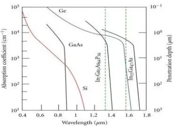
With the increase in depletion width due to reverse, capacitance of the depletion region increases due to which bandwidth increases. In most cases, detectors can have larger responsivity, but it will also increase both the dark current and the capacitance and hence reduces the sensitivity and the bandwidth, respectively. Semiconductor materials, such as Ge, Si, and III-V material, like GaAs, InP, have been used for the manufacturing of hetrojunction photodetectors. Figure(8) describe the
comparison of the absorption coefficients of different semiconductors including Silicon. From this fig(8) it can be seen that Si and GaAs have very low absorption coefficient while Ge and some other III-V materials have considerable absorption coefficient.
Fig. 8 Absorption coefficient as a function of their wavelength. The green dashes mark typical wavelengths for telecommunications windows
of 1310 and 1550 nm
7.1 Silicon Detector
From the fig (8) it is clear that Si exhibit transparency in the 1300–1550 nm operating wavelength range due to its low absorption coefficient it is not a satisfiable material for fiber-optic communication application. But it carry out well under 1000nm, where band-to-band absorptions happen. To solve this problem, we can approach to three structures; III-V heterogeneous detectors, Schottky structure or Ge detectors built on silicon substrates.
8. Schottky Detectors
ISSN 2348 – 7968
the asymmetric Surface Plasmon polaritions photodetectors.
Fig. 9 Scheme diagram of examples of (a) symmetric and (b) asymmetric surface Plasmon Schottky contact detector.
9. Heterogeneous Detector
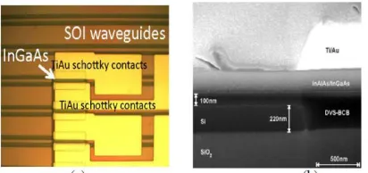
Compared to silicon III-V-based detectors III-V semiconductors have direct band gap and have wider absorption bandwidth as well as relative low dark currents. The lattice structures of III-V materials are different from the Si semiconductor hence these semiconductor materials cannot be directly grown on silicon. A solution to this problem is the heterogeneous to use a integration of III-V layers on silicon substrate by using advanced wafer bonding technique. In earlier the III-V detectors (GaAs,) are not compatible with CMOS (Complementary metal oxide semiconductor’s) technology approach. But in now a days some of them, like InGaAs/InP built on the SOI substrate using heterogeneous integration approach. This integration process achieved by using the DVS-BCB by adhesive die-to-wafer bonding process. In figure the metal-semiconductor-metal photo detector (MSM) using an InGaAs absorption layer were envision. The vertical directional coupling between the SOI waveguide and the lossy III-V waveguide mode Coupling is formed between the SOI waveguide and photo detector. At a bias voltage of 5v the dark current was formed of 3.0nA while the responsivity of detector was at 1.0A/W at 1.55 μm and bias voltage of 5V.
Fig. 10 (a) Top view of the fabricated III-V metal-semiconductor-metal photodetectors integrated on an SOI waveguide platform (b)
cross-section of the device.
10. Germanium Detector Built On Silicon
Ge has an indirect bandgap structure which similar to Si but having less band gap energy (0.7ev versus 1.1ev for Si) compared to Si. Hence it has a higher absorption coefficient up to the wavelength of 1550nm.
The present period of time most of the researchers are
ISSN 2348 – 7968
type (2) waveguide type this are the two structures of Ge-on-Si p-i-n photo detectors. On the basis of quantum efficiency and bandwidth waveguide based photo detectors are better than normal-incidence photo detectors. The induced type detectors have larger area, about ten times that of the waveguide detectors. The large progress is going on Ge on Si photo detectors. Vivien et al. gives the Ge detector with bandwidth of 42 GHz and responsivity at 1 A/W operating at 1550 nm wavelength. Ge detector with 17.5GHz bandwidth is showed by Feng et al. The bias voltage across the detectors, reduce the dark current, power absorption and operating voltage of chip are lowered by theCMOS integration process. Ge detectors of 130 nm and 180 nm respectively integrated with CMOS technology Currently has, a zero bias Ge detector with 17.5 GHz has been recently demonstrated by demonstrated by Luxtera and MIT. Ge detector with high sensitivity at 4 dB and speed at 10Gb/s is reported by Kang group in 2010.
11. Avalanche Photodetector
Avalanche photodiode detectors (APD) have great sensitivity and they exhibit larger gain bandwidth product as compare to that of the p-i-n type detectors. As compare to the the III-V detectors Ge-on-Si APD gives us better performances. Due to multiplication of charge carrier’s number of charge carriers increases by 10-100 factor in an avalanche based photodetectors. Thus it helps in the increases the sensitivity, bandwidth and helpul in long distance transmission. For low cost with Ge-on-Si APD at data rate of 40Gbps Progress work going on the development. 340 GHz gain–bandwidth with Ge–Si avalanche photodiode using CVD growth of Ge and Si layers at 850°C has been demonstrated by the Intel-UCSB team in the recent events.
12. Applications and Future Aspects
Recently Silicon photonics is extremely powerful technology which fulfills the demands for efficiency, higher speed, and low power consumption at lower costs. In silicon technology, using narrow waveguides various opto-electronics devices alliance on a single substrate connected with each other. Such circuits could be used to establish increased bandwidth, high speed transmission, reduced power consumption and decreasing latency problems. by providing micro-scale, ultra low power devices it can potentially increase the bandwidth capacity. Optical data transmissions increase the data rate and
exclude the complication of electromagnetic interference. With these data rates one could imagine the videoconferencing with a high resolution. Optical link can transfer data to longer distances and faster than today’s copper technology; up to 50 GB of data per second. Recently, Intel Corporation launched their optical link connection operating at 100Gbps. Fujitsu Laboratories recently create four wavelength integrated silicon laser for optical transrecievers. Work is in the progress for the new optic-interconnection of external devices to PCs. Intel announced Light Peak, 2009 which substitutes the USB and communicates the data at up to 10Gbps. Breakthrough in the field of silicon nanophotonic technologies leads new ideas in future computing systems and their architectures.
Refrences
[1] Ashish Dhiman, “Silicon Photonics: A Review,” e-ISSN: 2278-4861. Volume 3, Issue 5 (Mar. - Apr. 2013), PP 67-79. [2] Kilby, J.S., “Invention of the integrated-circuit,” IEEE Trans. Electron Devices, ED-23, 648–654, 1976.
[3] Soref, R.A., and Bennett, B.R., “Electrooptical effects in silicon,” IEEE J.Quant. Electron., QE-23, 123–129, 1987. [4] Tang, C.K., Kewell, A.K., Reed, G.T., Rickman, A.G., and Namavar, F., “Development of a library of low-los silicon-on-insulator optoelectronic devices,” IEE Proc. Optoelectron., 143, 312–315, 1996.
[5] Liu, A., Jones, R., Liao, L., Samara-Rubio, D., Rubin, D., Cohen, O.,Nicolaescu, R., and Paniccia, M., “A high-speed silicon optical modulator based on a metal-oxide-semiconductor capacitor,” Nature, 427, 615–618, 2004.
[6] Reed G., and Knights, A.P., Silicon Photonics: An Introduction, Wiley, New
York, (2004).
[7] Pavesi, L., and Lockwood, D.J., Silicon Photonics, Springer-Verlag, Berlin, (2004).
[8] Analui, B., Guckenberger, D., Kucharski, D., and Narasimba, A.,“A fully integrated 20Gb/s optoelectronic transceiver implemented in a standard 0.13 micron CMOS SOI technology,” IEEE J. Solid-State Circuits, 41, 2945–2955, 2006.
First Author Mr. Akshaykumar S.Hedaoo is pursuing his full time
bachelor’s degree in Electronis & telecommunication from JDIET Yavatmal. His area of interest is in Photonics system.
Second Author Prof. Atul N.Shire Received M.Tech degree in
Electronics from G.H.Raisoni, Nagpur, India in 2010. He has in all experience of 10 years in teaching & industry. He also served as Head of department for three years in DBNCOET in Electronics & Telecommunication, yavatmal, Maharashtra. Till date he has published 18 research paper in various International Journals/ Conference. His area of intrest is signal/image processing. He is also a life member of ISTE and IETE.
Third AuthorProf. Atul P.Shingade has completed his masters from