A Novel Method from Bandpass to Dual-Band for Microwave Filter
and Diplexer Design
Feng Qiu, Zhenghua Tang, Jianquan Huang*, Dajun Lei, and Ming Yao
Abstract—A novel method for a dual-band filter and quad-channel diplexer design is presented in this paper. This method, by altering the gap between resonators, realizes a transformation from bandpass to dual-band for the filter and diplexer. At first, a high selectivity bandpass filter (BPF) with four controllable transmission zeros (TZs) is designed. Then altering the gap between resonators, a band gap is generated and utilized to split the passband of the proposed BPF into two bands, which transform the BPF to a dual-band filter with a narrow passband separation. The center frequency and bandwidth of the new dual-band filter are controllable by adjusting the frequency and width of the band gap. Based on the dual-band filter, a quad-channel diplexer with stepped impedance T-junction is designed, and it can be transformed to a wideband diplexer. For demonstration, the dual-band filter and quad-channel diplexer are fabricated and measured.
1. INTRODUCTION
In the modern wireless communication devices, especially for smart cellphone, huge demand for high-performance filter and diplexer has motivated great efforts on their design. Frequency selectivity is always a concerned factor in the design process. To obtain a high selectivity, high orders of filters are needed. However, it will result in a gigantic size. Multi-mode resonator as a candidate may be utilized to reduce the size due to the coexistence of multiple modes in itself without decreasing the resonator orders [1–4]. Nonetheless, coupling coefficients between resonators are too hard to control, which makes it difficult to obtain a high performance. Besides, transmission zero (TZ) is another way to enhance the frequency selectivity and is generated by two major ways. One is the cross coupling among multiple paths with 180-degree phase differences between the source and the load [5–7]. The other is to add one-quarter wavelength open-stub on coupled input and output lines to form 0-degree feed line structure [8, 9].
High orders of filters and multiple TZs are always adopted in diplexer design to improve the isolation. However, in quad-channel diplexer design, high isolation is difficult to obtain since the passband separation of the dual-band in one channel is too large to satisfy both two passband. In [10], two pairs of dual-band filters using stepped impedance resonator are directly combined for quad-channel diplexer. Although multiple TZs generated by source-load coupling improve the selectivity of dual-band filter channels, the large passband separation of upper dual-band channel still leads to a low isolation between output ports.
In this paper, four half wavelength resonators are arranged as a nested structure to construct a compact high selectivity BPF. The total dimension of the proposed filter is similar to the BPF using dual-mode resonator [1, 2], but easier adjustment of coefficient is obtained as a result of the single-mode resonator. By combining cross coupling and a 0-degree feed line structure, two pairs of controllable transmission zeros are generated at both sides of the passband to enhance the frequency selectivity.
Received 6 August 2015, Accepted 18 September 2015, Scheduled 22 October 2015
* Corresponding author: Jianquan Huang ([email protected]).
With a slight alteration on the gap between resonators, a band gap is generated to split the passband of the proposed BPF into two bands, which transform the BPF to a dual-band filter. The newly transformed dual-band filter also owns high selectivity for two pairs of TZs generated by the 0-degree feed line structure and band gap. The center frequency and bandwidth of each band are easier to control than the multimode dual-band filter in [3, 4]. Moreover, the dual-band filter is created by splitting a passband into two bands. So the separation between the two passbands is small, and it is suitable for dual-band filter design with narrow passband separation. Exploiting the high selectivity and narrow passband separation of the dual-band filter, a quad-channel diplexer with stepped impedance T-junction is designed, and a better isolation is obtained than the corresponding results in [10].
2. BPF TO DUAL-BAND FILTER TRANSFORMATION
Figure 1 shows the layout of the proposed filter. It consists of four half wavelength resonators which construct a compact nested structure. The method from bandpass to dual-band is realized by adjusting the gaps g1 and g2.
(a)
(b)
(c)
Figure 1. (a) The structure of BPF and dual-band filter. (b) The coupling topology of BPF. (c) The coupling topology of transformed dual-band filter.
2.1. Bandpass Filter
Depending on the arrangement of four half wavelength resonators, the topology of BPF is obtained as shown in Fig. 1(b). The two outer resonators are appointed as Re1 and Re4, and the inner resonators are designated as Re2 and Re3.
Re1 and Re4 are coupled at the end of the microstrip line where the electric field is strongest. So the coupling is electrical coupling, and the coupling coefficientk1,4 is negative. Meanwhile, other couplings
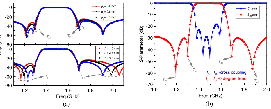
between resonators are at the center of the microstrip line where the magnetic field is strongest. So they are magnetic coupling, and the coupling coefficients are positive. This kind of cross coupling topology shown in Fig. 1(b) can generate a pair of transmission zeros (TZ2 and TZ3) near the passband since the two paths have 180-degree phase difference from source to load. TZ2 and TZ3 are controlled by coupling coefficientk1,4in the topology. Besides, 0-degree feed line is adopted to introduce another pair
-80 -60 -40 -20 0 -80 -60 -40 -20 0 Tz4 Tz1 Tz3 Tz2 -70 -60 -50 -40 -30 -20 -10 0 S -Parameter (dB) Tz1 Tz2 Tz3 Tz4 T z2, T z3-cross coupling
T z1, T z4-0 degree feed
1.2 1.4 1.6 1.8 2.0
Freq (GHz)
1.2 1.4 1.6 1.8 2.0
Freq (GHz) 1.0
dB[
S
(2,1)]
d = 1.8 mm d = 2.8 mm d = 3.8 mm
1 g = 0.5 mm g = 0.6 mm g = 0.7 mm
2
2 2
1 1
S 11sim
S 21sim
(a) (b)
Figure 2. (a) The variation of TZs. (b) The results of BPF.
the microstrip line. By combining cross coupling and 0-degree feed line, four TZs near the passband of BPF are generated to enhance the frequency selectivity. The variation of TZs is illustrated in Fig. 2(a). It can be observed that Tz2 and Tz3 move away from the center frequency withg2 increasing and Tz1 and Tz4 moving towards center frequency with d1 increase.
The normalized coupling matrix with return loss of 20 dB can be synthesized as shown in matrix (1). Depending on the structure and coupling matrix, a BPF with center frequency at 1.5 GHz and relative bandwidth of 13.3% is designed and simulated. The result is presented in Fig. 2(b).
⎡ ⎢ ⎢ ⎢ ⎢ ⎢ ⎣
0 1.07 0 0 0 0
1.07 0 0.93 0 −0.18 0
0 0.93 0 0.76 0 0
0 0 0.76 0 0.93 0
0 −0.18 0 0.93 0 1.07
0 0 0 0 1.07 0
⎤ ⎥ ⎥ ⎥ ⎥ ⎥ ⎦ (1)
2.2. Dual-Band Filter
Based on the proposed BPF above, a transformation from BPF to dual-band filter is obtained by the gaps alteration of inner resonators and outer resonator. When gap g1 between Re2 and Re3 increases
sufficiently, the coupling between them can be ignored. The topology of the proposed structure is renovated and shown in Fig. 1(c). The normalized coupling matrix of dual-band BPF with return loss of 20 dB is synthesized as shown in matrix (2). Compared with matrix (1), it can be seen that the coupling magnitude of k1,4 and k4,1 increases from −0.18 to −1.18, and the coupling coefficients k2,3
and k3,2 turn to be zero. The coupling coefficient k2,3 is nearly zero due to the huge gap between the
inner resonators. Furthermore, the coupling coefficient k1,4 needs to increase in order to ensure the
coupling magnitude of the only path between the source and the load. This kind of topology can realize a dual-band filter by splitting a passband into two bands.
⎡ ⎢ ⎢ ⎢ ⎢ ⎢ ⎣
0 1.07 0 0 0 0
1.07 0 0.93 0 −1.18 0
0 0.93 0 0 0 0
0 0 0 0 0.93 0
0 −1.18 0 0.93 0 1.07
0 0 0 0 1.07 0
⎤ ⎥ ⎥ ⎥ ⎥ ⎥ ⎦ (2)
The center frequency of each band can be controlled by coupling coefficient k1,4 which is controlled by
-70 -60 -50 -40 -30 -20 -10 0
27 28 29 30 31 32
-40 -30 -20 -10 0
(a) (b)
1.2 1.4 1.6 1.8 2.0
Freq (GHz) 1.0
S
-Parameter (dB)
g = 0.4, g = 1.3
1
g = 3.0, g = 1.3
g = 3.0, g = 0.8
g = 3.0, g = 0.2
2
1 2
1 2
1 2
L = 27.5 mm2 L = 28.5 mm L = 29.5 mm L = 30.5 mm L = 31.5 mm
2 2
2 2
First band Second band
L2 (mm)
S
-Parameter (dB)
Bandwidth (MHz)
160
120
80
40
1.3 1.4 1.5 1.6 1.7
Freq (GHz)
Figure 3. (a) The transmission parameters vary fromg1 and g2. (b) The bandwidth varies from L2.
gap g1 increases from 0.4 mm to 3 mm, a band gap splits the passband of BPF into two symmetric passbands. When gap g2 decreases from 1.3 mm to 0.2 mm, these two symmetric passbands move away from the center frequency of BPF. The bandwidth of each band is also controllable by setting the total length of the inner resonator. Fig. 3(b) depicts the bandwidth versus length L2. When length L2 increases from 27.5 mm to 31.5 mm, the band gap moves towards lower frequency, which leads to the decreasing bandwidth of the first band while the bandwidth of the second band increases. These two bandwidths are equal when L2 = 29.5 mm. The same as the proposed BPF, the 0-degree feed line structure introduces a pair of TZs. And the band gap generates another couple of TZs to enhance the selectivity of each passband.
The transformation procedure from BPF to dual-band filter can be summarized as below:
1. Based on the proposed BPF, increasing the gap g2 in order to avoid the coupling between inner resonators.
sim mea
S21 S11
Tz2
Tz4
Tz1
Tz3
(a) (b)
1.5 2.0
Frequency (GHz) 1.0
-50 -40 -30 -20 -10 0
S
-Parameter (dB)
Figure 4. (a) The results of symmetric dual-band filter. (b) The photography of dual-band filter (L1 = 31.7 mm, L2 = 30.55 mm, L3 = 6.9 mm, L4 = 14.85 mm, L5 = 7.2 mm, L6 = 10.7 mm,
L7 = 4.2 mm, d1 = 2.8 mm, d2 = 1.5 mm, d3 = 0.59 mm, g1 = 3 mm, g2 = 0.2 mm, W0 = 2.7 mm
2. Decreasing gapg1 to enhance the coupling of k1,4.
3. Adjusting the total length of resonators since the gap adjustment above may cause frequency shifting.
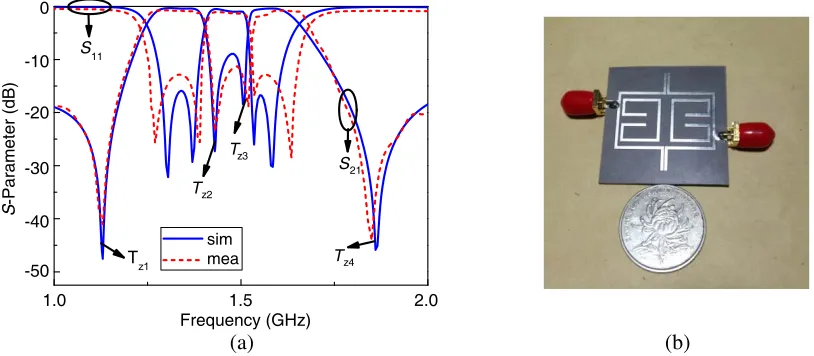
The dual-band filter is designed by splitting a passband into two bands. So the separation between the two passbands is small due to the limit of gap g2. With this property, it is suitable for dual-band filter design with narrow passband separation.
Based on the BPF above, a dual-band filter with center frequency at 1.4 GHz/1.6 GHz is designed and implemented on a substrate with a thickness of 1 mm, relative dielectric constant of 2.55, and loss tangent of 0.001. The result is shown in Fig. 4.
3. QUAD-CHANNEL DIPLEXER DESIGN
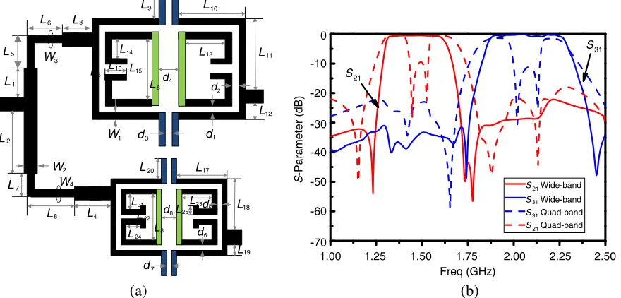
Based on the dual-band filter, a quad-channel diplexer with stepped impedance T-junction is designed, and the structure is shown in Fig. 5(a). It includes two parts of the dual-band filter with center frequency at 1.4 GHz/1.6 GHz and 1.95 GHz/2.2 GHz.
5 L 8 L 5 L 8 L 1 L 2 L 3 L 4 L 9 L 6 L 11 L 12 L 13 L 14 L 15 L 20 L L L 23 L 22 L 17 L 21 L 1 d 2 d 3 d 4 d 5 d 6 d 7 d 8 d 1 W 2 W 5 L 10 L 7 L 8 L 16 L 24 L 25 L 3 W 4 W -70 -60 -50 -40 -30 -20 -10 0 S21 S -Parameter (dB) S31 (a) (b)
1.25 1.50 1.75 2.00 2.25 Freq (GHz)
1.00 2.50
S Wide-band
S Wide-band
S Quad-band
S Quad-band
21 31 21 31 18 19
Figure 5. (a) The structure of dual-band diplexer. (b) Comparison between diplexer and quad-channel diplexer.
Direct combining of two dual-band filters may result in bad performance. So optimization based on initial dual-band filter parameters is needed. The first resonators of the two channels need slight optimization since they are directly linked with a junction network. The initial length of the T-junction network from the input port to the first resonator of each channel is usually assigned as one-quarter guide wavelength of the other channel in diplexer design. But in the quad-channel diplexer design, each channel consists of two passbands, which makes it hard to determine the frequency of the guide wavelength. In this work, stepped impedance T-junction is taken to optimize for dual-band isolation. Besides, passband separations of dual-band in each channel are 200 MHz/250 MHz which are narrow separation, so it is easier to obtain a good isolation than the quad-diplexer in [10]. The ratio of stepped impedance and length is optimized by software ADS to obtain a good isolation and matching. The quad-channel diplexer can also be transformed into a wideband diplexer with the gap alteration of inner and outer resonators. And the T-junction needs to optimize again for wideband diplexer. In Fig. 5(b), results comparison between wide-band diplexer and quad-channel diplexer is shown.
-70 -60 -50 -40 -30 -20 -10 0
(a) (b)
1.5 2.0 2.5
Freq (GHz) 1.0
S
-Parameter (dB)
-80
1.5 2.0 2.5
Freq (GHz) 1.0
-70 -60 -50 -40 -30 -20 -10 0
S
-Parameter (dB)
-80
-90
S21 S31
S23
S11
-35 dB
S sim
31
S sim
21
S mea
S mea
31 21
S sim
S sim
S mea
S mea
23 11
23 11
Figure 6. The results of quad-channel diplexer. (L1 = 6.15 mm, L2 = 15.26 mm, L3 = 3 mm,
L4 = 3 mm, L5 = 4.345 mm, L6 = 5 mm, L7 = 14.87 mm, L8 = 6.93 mm, L9 = 6.9 mm,
L10 = 14.852 mm, L11 = 14.4 mm, L12 = 2.8 mm, L13 = 10.69 mm, L14 = 4.2 mm, L15 = 12.9 mm,
L16 = 8.2 mm, L17 = 10.852 mm, L18 = 10.44 mm, L19 = 2.46 mm, L20 = 5.1 mm, L21 = 3.2 mm,
L22 = 9.1 mm, L23 = 6.69 mm, L24 = 4 mm, L25 = 2 mm, d1 = 1.5 mm, d2 = 0.6 mm, d3 = 0.2 mm,
d4 = 3.328 mm,d5 = 0.79 mm,d6 = 1.3 mm,d7= 0.296 mm,d8 = 3.024 mm,W1= 1 mm,W2 = 2.7 mm,
W3= 1.65 mm,W4 = 2.5 mm).
better isolation due to the narrow passband separation in each dual-band channel compared with the quad-channel diplexer in [10].
4. METHOD APPLICATION
In the above sections, the method of splitting one band into two passbands by a band gap is built on a four-order BPF with a nested structure. The limitation of filter orders seems to restrict the application of this method. To extend this method to higher-order, two approaches can be adopted.
(1) More resonators can be incorporated into the interior space. As shown in Fig. 7(a), four
(a)
(b)
(c)
inner resonators and two outer resonators construct a sixth-order BPF. By altering the gap of outer resonators and inner resonators, a transformation from sixth-order BPF to three-order dual-band filter can be achieved. The coupling topology transformation is shown in Fig. 7(b) and Fig. 7(c). However, due to the restriction of interior space, this approach is restricted to six-order.
(2) Multi-mode resonator such as the SIR (stepped impedance resonator) and SLR (stub-load resonator) may be adopted to realize a higher-order BPF.
5. CONCLUSION
In this paper, a method from bandpass to dual-band for filter and diplexer is presented. A high selectivity BPF is designed at first. Based on the proposed filter, a dual-band filter is transformed by gap alteration of resonators. Exploiting the high selectivity and narrow passband separation of proposed dual-band filter, a quad-channel diplexer with stepped feed line is designed and fabricated.
ACKNOWLEDGMENT
This work was supported by the Aid Program for Science and Technology Innovative Research Team in the Higher Educational Institutions of Hunan Province.
REFERENCES
1. Chiou, Y.-C., P.-S. Yang, J.-T. Kuo, and C.-Y. Wu, “Transmission zero design graph for dual-mode dual-band filter with periodic stepped-impedance ring resonator,” Progress In Electromagnetics Research, Vol. 108, 23–36, 2010.
2. Zhang, X.-S., Y.-J. Zhao, H.-W. Deng, L. Zhang, and W. Chen, “High selectivity dual-mode bandpass filter with source-loaded coupling,” Progress In Electromagnetics Research Letters, Vol. 18, 187–194, 2010.
3. Guo, L., Z.-Y. Yu, and L. Zhang, “Design of a dual-mode dual-band filter using stepped impedance resonators,”Progress In Electromagnetics Research Letters, Vol. 14, 147–154, 2010.
4. Weng, M.-H., S.-K. Liu, H.-W. Wu, and C.-H. Hung, “A dual-band bandpass filter having wide and narrow bands simultaneously using multilayered stepped impedance resonators,” Progress In Electromagnetics Research Letters, Vol. 13, 139–147, 2010.
5. Thomas, J. B., “Cross-coupling in coaxial cavity filters — A tutorial overview,” IEEE Trans. Microwave Theory Tech., Vol. 51, No. 4, 1368–1376, 2003.
6. Ma, Z., T. Asano, and Y. Kobayashi, “Theory for the design of a filter having one cross coupling path to realize transmission zeros,”IEICE Transactions on Electronics, Vol. 86, No. 8, 1690–1698, 2003.
7. Chu, Q. X., F. C. Chen, Z. H. Tu, and H. Wang, “A novel crossed resonatorand its applications to bandpass filters,”IEEE Trans. Microwave Theory Tech., Vol. 57, 1753–1759, 2009.
8. Qiu, F., L. Z. Zhang, and B. Wu, “High selective dual-band microstrip filter using zero-degree coupled SIR feed lines,” 2014 3rd Asia-Pacific Conference on IEEE Antennas and Propagation (APCAP), 731–733, 2014.
9. Feng, W., X. Gao, W. Che, and Q. Xue, “Bandpass filter loadedwith open stubs using dual-mode ring resonator,”IEEE Microwave and Wireless Components Letters, Vol. 25, No. 5, 295–297, May 2015, doi:10.1109/LMWC.2015.2410174.