IJEDR1303009 INTERNATIONAL JOURNAL OF ENGINEERING DEVELOPMENT AND RESEARCH | IJEDR Website: www.ijedr.org | Email ID: [email protected] 39
Comparative Performance Analysis of XOR-XNOR
Function Based High-Speed CMOS Full Adder Circuits
1Bhavani Prasad Y., 2Harish Babu N., 3Ramana Reddy K.V., 4Dhanabal R. Sense School, VIT University, Vellore, Tamilnadu
1
[email protected], [email protected]@gmail.com , [email protected]
Abstract— this papers presents the realization of full adder designs using Complimentary CMOS Design, Complimentary Pass Transistor Logic Design and XOR-XNOR Design in a single unit. The main motive of this paper is to determine the comparative study of power, delay, power delay product (PDP) of different Full adder designs using CMOS Logic Styles. Simulations results clearly determines that XOR-XNOR type Full adder Design is better compared to Complimentary CMOS style and Pass Transistor Design with respect to power, delay .Power Delay Product Comparison .The power delay product is also important parameter to determines the performance of the design. The XOR-XNOR implementation provides better performance and requires less number of transistors compared to other full adder designs. The implementation of design using GPDK 180nm with supply voltage of 1.8 V in Cadence Virtuoso Schematic Composer and simulations done by using Spectre Environment
Index Terms — XOR, Full adders, XNOR, PTL, XOR-XNOR.
I. INTRODUCTION
Power consumption and delay are two important considerations for VLSI system designer engineers. Our prime motive is to reduce the power and to get less delay that is nothing but the high speed for any design. Adder is one of the fundamental block present in arithmetic logic unit (ALU), floating point unit .In present arena we need fast arithmetic computation cells like adder and multipliers in the very large scale integration (VLSI) designs. The XOR/XNOR is the basic building block in many circuits like Arithmetic circuits.
Compressors, Comparators, Phase detectors, Code converters, Multipliers, Parity Checkers, Error-detecting and Error-correcting codes. Moreover, adders are very important components in some other applications such as microprocessor and digital signal processing (DSP) architectures. Digital signal processors and Microprocessors mainly rely on highly efficient implementations of generic floating point units and arithmetic logic units(ALU).
Full Adder is one of the core element in many of the complex arithmetic logic circuits like multiplication, division, addition, exponentiation, etc. To perform an arithmetic operation, mainly even a small circuit can consume very low power at extremely low frequency and also it may even take a long time to complete that operation. There are some standard implementations.
Some different logic styles have been used in the past times for design of the full-adder cells[5]-[19] and those techniques are used in this paper. Although they are used for producing similar function and the way of producing transistor count and intermediate nodes are varied. Different logic styles have different advantages such as the size, power dissipation, speed and the wiring complexity of the circuit. Different logic styles have different performance aspects. The propagation delay of a circuit is determined by the number of inversion levels, number of transistors in series, the transistor sizes or channel widths and the intra cell wiring capacitances. The size of the circuit depends on the number of transistors and their sizes and also on wiring complexity of the circuit. In order to get switching point to half of VDD proper sizing should have to be done [1]-[4].
Some may use only one logic style for whole full adder while others can use more than one logic style for their implementation. II. BACKGROUND
Power is the main criteria in all the electronic design equipment’s. So that’s why the designers are trying to minimize the power consumption when designing the task. In CMOS circuits mostly the energy consumed is because of switching activity. Thus the number of nodes in the circuit, energy per every node and also the total number of transaction operations per second, all these factors led to the power consumption. Power dissipation is based on the node capacitances of gate, threshold switching activity and circuit size.
There are four reasons for the power dissipation: dynamic power due to the charging and discharging of capacitance in the circuit because of switching transactions and leakage current is because of reverse bias condition in diode structures, sub threshold leakage, short-circuit current power due to rise and fall times, and static biasing power found in some logic styles (i.e pseudo-NMOS) These three are the major components of power dissipation in (CMOS) circuits:
1. Dynamic Power: Power consumed by the circuit node capacitance because of transistor switching.
IJEDR1303009 INTERNATIONAL JOURNAL OF ENGINEERING DEVELOPMENT AND RESEARCH | IJEDR Website: www.ijedr.org | Email ID: [email protected] 40
The increase in demand for low power and low voltage VLSI circuits can be investigated different levels of design, such as the architectural, circuit, layout and the process technology. At the device level, reduction in supply voltage and reduction in the threshold voltage to reduce the power consumption, where as in layout use of short channel transistors, poly and diffusion areas, shorter metal lines for connecting two various devices. It reduces capacitances in circuit and device level.
On an architectural level, CAD algorithms are required for fewer number of gates which reduces the overall power consumption. All these techniques employed most of the times reduce power increase of delay [1]-[5].
(A) Complementary CMOS Full Adder(C-CMOS):
The complementary CMOS full adder (C_CMOS) is one of the basic full adder circuit shown in below fig .1(a)
Fig.1(a) C-CMOS Full Adder Cell[3]. The equation for C-CMOS is given as below
Sum =Carry'.(A+B+C) + (A.B.C) Sum = ABC + AB'C' + A'BC' + A'B'C & .
From the equation we have drawn the pull up and pull down networks and from that we have generated the sum and carry outputs. The advantages of the complementary CMOS logic circuit are stability and layout regularity at lower voltages due to smaller number of interconnecting wires and complementary pairs of transistors. The C_CMOS have some robustness against transistor sizing and voltage scaling which can have reliable operation at very low voltages with different transistor sizes.
The second adder is complementary pass transistor logic (CPL) uses 32 transistors with swing restoration. Most CPL gates can have an complexity in interconnection at the layout level with the increase in power and delay. For low power applications Pass Transistor Logic (PTL) is best suitable technique and explanation was given in .The advantage of Pass Transistor Logic (PTL) is that either PMOS or NMOS is enough to implement a complete design [6]-[8] and so number of transistors gets decreased and also smaller input loads, especially for NMOS network and also by this PTL we can eliminate short circuit energy dissipation.
(B)3T XOR:
The modified model of a CMOS inverter and a PMOS pass transistor. Whenever the input B is of logic 1 or logic 0, then the inverter functions like a normal CMOS inverter. And the output Y is the inverter of input A. Whenever the input B is at logic 0, the CMOS inverters output is at high impedance(z). However transistor N3 is in on condition and the output Y gets the same value as input A.
IJEDR1303009 INTERNATIONAL JOURNAL OF ENGINEERING DEVELOPMENT AND RESEARCH | IJEDR Website: www.ijedr.org | Email ID: [email protected] 41
Another problem is current back through transistor N1 occurs when A=1 and B=0. The output of the pass transistor is fed back through transistor N1 which it operates in the active region. This can overcome by reducing the W/L ratio of transistor N1.
(C) 8T ADDER USING XOR GATE:
The 8T adder is implemented using 3T Xor gates The sum output is basically obtained by a implementing exclusive OR of the three inputs in The final sum of the products is obtained using a OR logic of PTL type[15].
Thus two stage are required to obtain the sum value as output and at most in both the stage delays are to be added. The voltage drop due to the threshold in the transistors M3 and M6 can be reduced by increasing the aspect ratios of the transistors. The input combinations of all the three inputs have been checked by taking the rise and fall time into considerations. The 8-T XOR based Full Adder is shown in fig .2(b)
Fig.2(b)
XOR based Full Adder cell(D) 3T XNOR
IJEDR1303009 INTERNATIONAL JOURNAL OF ENGINEERING DEVELOPMENT AND RESEARCH | IJEDR Website: www.ijedr.org | Email ID: [email protected] 42
Fig.2(d) 3T XNOR Cell (E) 8T XNOR
It is implemented by two XNOR gates with one multiplexer block Sum is generated by using two XNOR gates, Carry out is generated by using two transistors multiplexer block. The XNOR gates with eight transistors has been implemented by using 3T XNOR gate, The simulation has performed form 3.0V to 1.2V to check the levels of output signal circuit in which it shows desired voltage levels. The 8T XNOR based Full Adder Cell was shown in below fig .2(d).
Fig.2(d)
XNOR based Full Adder cellIII. PROPOSED ARCHITECTURE
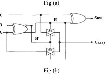
In this proposed adder we will use one XOR and one XNOR and a multiplexer to generate output sum and carry. The expressions for sum and carry are given in below.
Sum = H XOR C = H. C' + H'. C
Cout = A. H' + C. H
Sum = (A
B
C) = C' (A
B) + C (A
B)'
Where H is (A XOR B) and H' is compliment of (AXNORB).
IJEDR1303009 INTERNATIONAL JOURNAL OF ENGINEERING DEVELOPMENT AND RESEARCH | IJEDR Website: www.ijedr.org | Email ID: [email protected] 43
Fig.(a)
Fig.(b)
Fig.3 General Structure of proposed XOR-XNOR Adder[13].
In this proposed adder the two transmission gates are used as multiplexer and the sum can be generated by XOR gates and output carry can be generated by XOR /XNOR gates shown in the above figure and output of XOR gate can be used as the selection line for multiplexer or as the control for the transmission gate which we will get output as the carry. The proposed adder circuit is designed by the combination of the two logic styles in order to get lower power consumption, high speed and good energy efficiency. We know that supply voltage variations will leads to the greater reduction in the power and also in the circuit delay.
IV. EXPERIMENTAL RESULTS
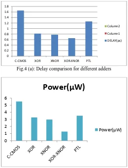
All the circuits presented in this paper are designed by using Cadence VIRTUOSO environment by using CMOS process design kit. The range of supply voltage we have employed was The proposed adder circuit is designed and simulated for different ranges of supply voltages is 1.3V-1.8V. The results of this proposed adder circuit can be compared with the different conventional adder circuit designs. Totally 16 transistors are needed to design the proposed adder circuit. By this we can clearly decide that the proposed circuit can have lower area overhead than the other conventional adder circuits. The delay values of conventional adder circuits and proposed adder circuit are compared and tabulated in below in table.1and table.2. and from the results it is clear that the proposed adder can have very less delay. The proposed circuit can have the lower power values and also lower PDP values as compared to other conventional adder circuits
Table 1 Simulation results for Full adder at VDD=1.3V
Type Power(µW)
C-CMOS 5.521
CPTL 3.52
XOR 3.265
XNOR 2.985
XOR-XNOR 1.295
Table 2 Simulation results for Full adder at 1.3V
Type Delay(
ps)
PDP # of
transisto rs
C-CMOS 1.65 9.10 28
CPTL 1.257 4.424 32
XOR 0.825 2.64 8
XNOR 0.785 2.345 8
XOR- XNOR
IJEDR1303009 INTERNATIONAL JOURNAL OF ENGINEERING DEVELOPMENT AND RESEARCH | IJEDR Website: www.ijedr.org | Email ID: [email protected] 44
Fig.4 (a): Delay comparison for different adders
Fig 4(b): Power Comparison results for different adders
Fig.4(c) Simulation input and output results for proposed adder
V. CONCLUSION
This paper includes the Implementation of different adder logic styles includes Complimentary CMOS, XOR-XNOR, Complementary Pass Transistor Logic and Simulated by using Cadence Environment .The Comparison of power, delay, PDP are tabulated. From the table it is clear that Complimentary CMOS Adder design having more power consumption and delay so more PDP. This paper includes a new adder design of XOR-XNOR based adder cell with less power, delay, and power delay product (PDP). Cadence simulations results can show that the new adder design have very less PDP when compared with all other designs.
0 0.2 0.4 0.6 0.8 1 1.2 1.4 1.6 1.8
C-CMOS XOR XNOR XOR-XNOR PTL
Column2
Column1
DELAY(ps)
0 1 2 3 4 5 6
Power(µW)
IJEDR1303009 INTERNATIONAL JOURNAL OF ENGINEERING DEVELOPMENT AND RESEARCH | IJEDR Website: www.ijedr.org | Email ID: [email protected] 45
The new full adder design can provide good voltage swing at low supply voltages and provides best performance with respect to all other conventional full adder designs in terms of both speed and power.
REFERENCES
[1] J. M. Rabaey, A. Chandrakasan, B. Nikolic, “Digital Integrated Circuits, A design Perspective,” 2nd Prentice Hall, Englewood Cliffs, NJ, 2002.
[2] J. Uyemura, “CMOS Logic Circuit Design,” Kluwer, 1999.
[3] Sung-Mo Kang, Y. Leblebici, “CMOS Digital Integrated Circuits: Analysis and Design,” Tata McGraw Hill, 2003. [4] N. Weste, D. Harris, “CMOS VLSI Design,” Pearson Wesley, 2005.
[5] R. Pedram, M. Pedram, Low Power Design Methodologies, Kluwer, Norwell, MA, 1996
[6] R. Zimmermann and W. Fichtner, “Low-power logic styles: CMOS versus pass transistor logic,” IEEE J. Solid-State Circuit, vol. 32, pp.1079-1090, July 1997.
[7] U.Ko,P.T.Balsara, W. Lee, “Low Power Design Techniques for High Performance CMOS Adders,” IEEE Trans. on VLSI System, vol. 3, pp. 327-333, June 1995.
[8] D. Radhakrishnan, “Low-voltage low-power CMOS full adder,” Proc.Inst. Elect. Engg. Circuits Devices Systems, vol. 148, no. 1, Feb.2001, pp. 19-24.
[9] C.H. Chang, J. Gu, M. Zhang, A review of 0.18um full adder performances for tree structure arithmetic circuits, IEEE Trans. Very Large Scale Integration (VLSI) Syst. 13 (6), June 2005.
[10] A. M. Shams, T. K. Darwish, and M. A. Bayoumi, “Performance Analysis of low-power 1-bit CMOS full adder cells,” IEEE Trans. Very Large Scale Integr. (VLSI) Syst., vol. 10, no. 1, pp. 20–29, Feb. 2002.
[11] S. Goel, Ashok kumar, M. A. Bayouni, “Design of Robust, Energy- Efficient Full Adder for Deep-Submicrometer Design Using Hybrid- CMOS Logic Style,” IEEE Trans. Very Large Scale Integr. (VLSI) Syst., vol. 14, no. 12, pp. 1309-1321, Dec. 2006. [12] Hanho Lee, G. E. Sobelman, “New XOR/XNOR and full adder circuits for low voltage, low power application,”
Microelectronics Journal vol. 29,pp. 509-517, 1998.
[13] M. Vesterbacka, “A 14-transistor CMOS full adder with full voltage swing nodes,” Proc. IEEE Workshop Signal Processing Systems, Oct 1999, pp. 713-722.
[14] J. Wang, S. Fang, and W. Feng, “New efficient designs for XOR and XNOR functions on the transistor level,” J. Solid State Circuits, vol.29, pp. 780-786, July 1994.
[15] H.T. Bui, Y. Wang, Y. Jiang, “Design and Analysis of low-power 10-transistor full adders using novel XOR-XNOR gates,” IEEE Transactions on Circuits & Systems II, vol. 49, pp. 25-30, Jan. 2002.
[16] S. Goel, M. E. Elgamel, M. A. Bayouni, Y. Hanafy, “Design Methodologies for high- performance Noise-tolerant XOR-XNOR Circuits,” IEEE Trans. Circuits and Syst. I, vol. 53, no. 4, pp. 867-868, April 2006.
[17] K. Navi, O. Kavehei, M. Rouholamini, A. Sahafi, S.Mehrabi, N.Dadkhahi, "Low-Power and High-Performance 1-bit CMOS FullAdder Cell," Journal of Computers, vol. 3,no. 2, pp. 48-54, Feb. 2008
[18] O. Kavehie, Mostafa Rahimi Azghadi, Keivan Navi and amir Pasha Mirbaha, "Design of Robust and High –Performance 1 Bit CMOS Full Adder for Nanometer Design," IEEE Computer Society Annual Symposium VLSI (ISVLSI), Montpellier Fr., 2008, pp. 10-15.