Design and Performance Analysis of High
Speed Low Power 1 bit Full Adder
Gauri Chopra1, Sweta Snehi2
PG student [RNA], Dept. of MAE, IGDTUW, New Delhi, India1
PG Student [VLSI], Dept. of ECE, IGDTUW, New Delhi, India2
ABSTRACT:In this Paper, design of high speed, low power 1-bit full adder using both logic gates and complementary metal oxide semiconductor (CMOS) logic is implemented. The main purpose behind designing this full adder is to reduce power and delay of standard implementation by replacing OR gate with XOR gate for output carry generation. The design proposed was first implemented using CEDAR logic tool and then with cadence virtuoso tool in 180nm technology. The simulation was carried out at 1.8V supply with length and width of each transistor taken as 0.18 μm and 2 μm. Performance parameters such as power, speed and design of existing full adder is compared with the proposed design. In comparison with the standard implementation of full adder, the present implementation was found to offer significant improvement in terms of power and speed.
KEYWORDS: Cadence virtuoso tool, CEDAR logic tool, CMOS, full adder design, high speed, low power.
I.INTRODUCTION
Most of the Very large scale integration (VLSI) applications such as voice and data communication network, image and video processing, microprocessors, microcontrollers, Microelectro mechanical systems (MEMS), cellular phones, and notebooks demand improved power delay characteristics. The aforementioned applications extensively use arithmetic circuits to perform arithmetic operations such as addition, subtraction, multiplication and multiply and accumulate (MAC). The 1-bit full adder is basic building block of these modules [1].
Thus it is necessary to enhance its performance for enhancing the overall performance of the module. The most important parameter for VLSI circuits is speed and power consumption. The higher power consumption of modules raises chip temperature which directly affects the battery life of modules [2]. Therefore, full adder which offers faster operation and consumes less power will enhance overall performance of module. In this paper, we represent 1-bit full adder which consumes less power and offer high speed as compared to standard implementation. The simulation is firstly carried out in CEDAR logic tool to verify and prove the logic, then in cadence virtuoso tool in 180nm technology at 1.8v to compare the power and delay of standard and proposed implementation.
The rest of this paper is organized as follows,in Section II related work is discussed, in Section III we review standard implementation of full adder. In Section IV we present the proposed 1- bit full adder. In Section V, we present simulation result of proposed and standard full adder. Finally Comparison of result will show superiority of proposed full adder.
.
II. RELATED WORK
inverters lead to fast switching speeds (224 ps at 1.8-V supply), for a layout area of 102.94 μm2 (in 180-nm technology) excluding buffer[6].
JayRam Shrivas et al. (2012) In this paper, the performance of the proposed 11T full adder circuit has been shown to outperform the 10T full adder, which can operate at low-voltages and have good output swings.The GDI(gate diffusion input) technique has been used for simultaneous generation of XOR gate. At the cost of negligible area overhead power consumption of 11t adder circuit is decreased approx. 42.47% at varying supply voltages. The proposed design can be suitable for low power application[2].
Shams, Ahmed M. et al. (2000) proposed and tested two novel design methodologies for noise-immune low voltage XOR–XNOR circuits. The performance of the proposed circuits has been shown to outperform the compared ones, which can operate at low-voltages, and have good output levels. The proposed circuits have been tested to have higher noise-immunity, higher energy-efficiency and faster operation than the compared ones. On an average, the savings in PDP ranges from 21% to 94% for a supply voltage range from 0.6 to 3.3 V, respectively [1].
S. Goel et al. (2006) proposed a novel low-power 1-bit full-adder cell. It uses the 4-transistor implementations of the XOR and XNOR functions, transmission gates, and pass transistors. Low power consumption is targeted at the circuit-design level. The cell is characterized by having no inverters and a balanced generation of the control signals of its transmission gates. It has a lower dynamic power component and no short-circuit [4].
III. STANDARD IMPLEMENTATION OF FULL ADDER
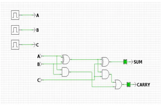
A full adder is one of the basic building block of digital circuits. Full adder is a combinational circuit with three inputs i.e. A, B, and C and two outputs i.e. SUM and CARRY[8]. Fig. 1. Shows logic circuit of standard full adder and TABLE I shows truth table of standard full adder.
Fig.1. Logic circuit of standard full adder
The SUM and CARRY generated is given as SUM = (A XOR B) XOR C
TABLE I
Truth table of standard full adder
Inputs Output
A B C SUM CARRY
0 0 0 0 0
0 0 1 1 0
0 1 0 1 0
0 1 1 0 1
1 0 0 1 0
1 0 1 0 1
1 1 0 0 1
1 1 1 1 1
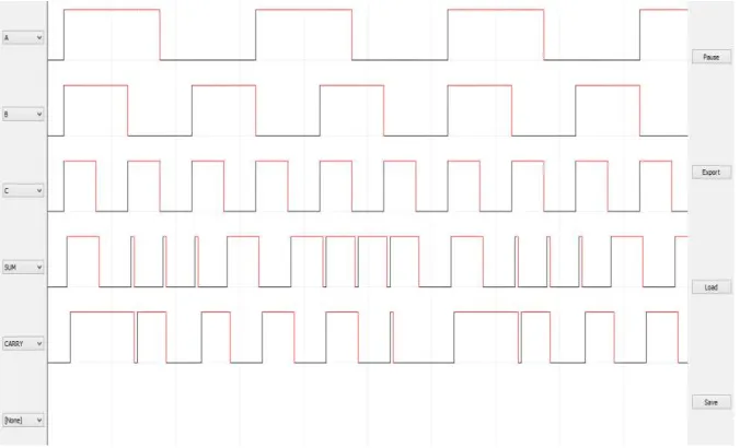
The output waveform of Standard full adder after simulation in CEDAR logic tool is shown in Fig. 2. In the mentioned figure, when inputs i.e A=1, B=1 and C=1 the following output i.e SUM = 1 CARRY =1 , similarly when inputs i.e A=1, B=1 and C=0 the following output i.e SUM = 0 CARRY =1 and so on .
Fig. 2. Waveform of standard full adder
IV. DESIGN OF PROPOSED FULL ADDER
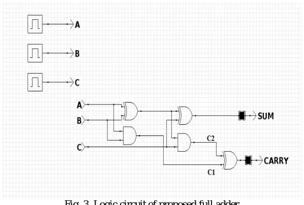
The logic circuit of proposed full adder is represented in Fig. 3. In this circuit, OR gate is replaced by XOR gate to generate final CARRY output. When either of the carry bit i.e. C1 or C2 is high , the final CARRY output is high.
The SUM and CARRY generated is given as SUM = (A XOR B) XOR C
CARRY = C1 XOR C2 Where
Fig. 3. Logic circuit of proposed full adder
TABLE II represents the truth table of proposed full adder. If we compare TABLE I and TABLE II of standard and proposed full adder, the functionality achieved by substituting XOR gate in place of OR gate is same as standard full adder. Therefore, XOR gate can be used to generate final CARRY output. Now the proposed and standard full adder logic circuits are implemented using CMOS logic in Cadence Virtuoso tool to compare the average power and delay generated. The circuits are implemented in 180nm technology with supply voltage as 1.8V.
TABLE II
Truth table of proposed full adder
Inputs Output
A B C SUM C1 C2 CARRY
0 0 0 0 0 0 0
0 0 1 1 0 0 0
0 1 0 1 0 0 0
0 1 1 0 0 1 1
1 0 0 1 0 0 0
1 0 1 0 0 1 1
1 1 0 0 1 0 1
1 1 1 1 1 0 1
Fig. 4. Waveform of proposed full adder
V. PERFORMANCE ANALYSIS OF PROPOSED FULL ADDER USING CMOS LOGIC
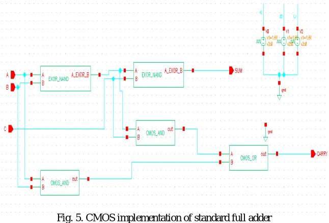
The simulation of the proposed and standard full adder is carried out with cadence virtuoso tool in 180nm technology with the aim to optimize both power and delay of the circuit. The power delay product i.e. energy consumption has been minimized in the proposed full adder. The implementation results provide significant improvement in power and delay. It was observed that in proposed full adder, propagation delay and power can be significantly minimized. Fig. 5. shows the CMOS logic implementation of standard full adder. When the CMOS circuit of standard full adder was simulated at 1.8V, it resulted in average power consumption of 62.84μwand propagation delay of 17.64ns.
Fig. 5. CMOS implementation of standard full adder
Fig. 6. Output waveform of Standard Full adder
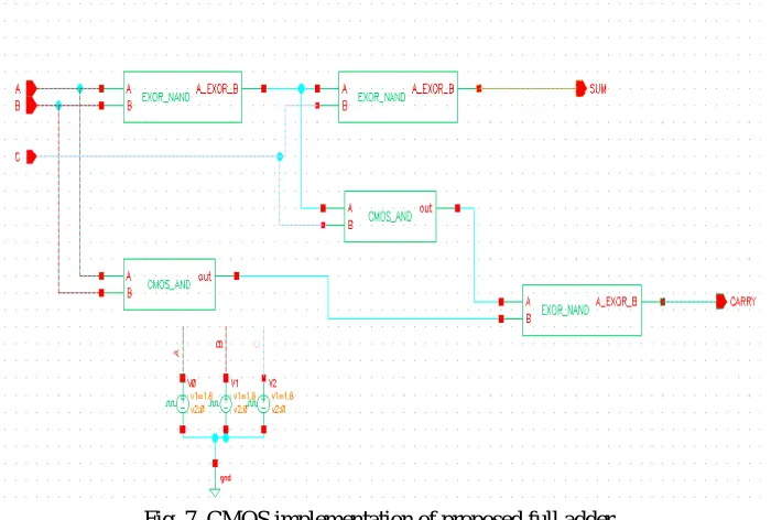
Whereas the Fig.7. represents the CMOS implementation of proposed full adder simulated in same environment resulting in average power consumption of 31.6μw and propagation delay of 12.19ns. In the CMOS circuit of proposed full adder the final CARRY output is generated by CMOS- EXOR gate. The proposed full adder offers low power consumption and minimized propagation delay. The power consumed by proposed full adder is approximately half of the power consumed by standard full adder.
Fig. 7. CMOS implementation of proposed full adder
Fig. 8. Output waveform of Proposed Full adder
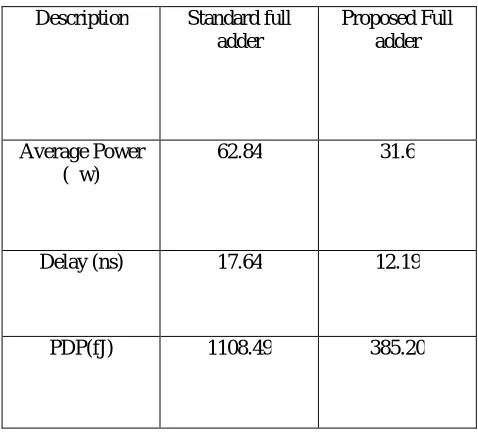
For the comparison in common environment the proposed and standard full adder, as cited in TABLE III offers variation in power consumption, propagation delay and corresponding PDP. The proposed full adder offers PDP of 385.20fJ whereas the standard full adder offers PDP of 1108.49fJ which is comparatively very high. The comparison between standard and proposed full adder depicts improvement in power , delay and superiority of proposed design.
TABLE III
Comparison of Average power and delay of proposed full adder and standard full adder.
Description Standard full adder
Proposed Full adder
Average Power (μw)
62.84 31.6
Delay (ns) 17.64 12.19
PDP(fJ) 1108.49 385.20
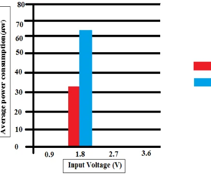
The graph shown in Fig. 9. represent that the proposed design of full adder has much better performance in terms of power consumption in comparison to standard full adder. It depicts that the proposed full adder is the viable option for efficient design as it offer high speed and low power consumption.
Fig. 9. Input voltage (V) vs average power consumption(μw)
VI.CONCLUSION
In this paper, high speed low power 1-bit full adder design has been proposed. The simulation was carried out using CEDAR logic tool and Cadence Virtuoso tool with 180nm technology at 1.8v and compared with standard full adder design. The simulation results offered by proposed full adder provide improved average power and delay thus resulting in improved PDP. The low power, high speed design of full adder shows the superiority over standard implementation. Further, this proposed design can be modified using hybrid techniques to lower power consumption and delay.
REFERENCES
[1] Shams, Ahmed M., and Magdy A. Bayoumi. "A novel high-performance CMOS 1-bit full-adder cell." IEEE Transactions on circuits and systems II: Analog and digital signal processing 47.5 (2000): 478-481.
[2] Shrivas, Jayram, Shyam Akashe, and Nitesh Tiwari. "Design and performance analysis of 1 bit full adder using GDI technique in nanometer era." Information and Communication Technologies (WICT), 2012 World Congress on. IEEE, 2012.
[3] S. Goel, M. A. Elgamel and M. A. Bayoumi, “Design Methodologies for High-Performance Noise-Tolerant XOR–XNOR Circuits,” IEEE Transl. on Circuits and Systems—I: Regular Papers, vol. 53, No. 4, April 2006.
[4] Q. Wu, P. Massoud, X.Yu, “Clock-Gating and Its Application to Low Power Design of Sequential Circuits,” Proc. of the IEEE Custom Integrated Circuits Conference, 1997, pp. 425-435.
[5] V. Gutnik, A. Chandrakasan, “Embedded Power Supply for Low-Power DSP,” IEEE Transl. on VLSI Systems, vol. 12, 1997, pp. 425-435. [6] Bhattacharyya, Partha, et al. "Performance analysis of a low-power high-speed hybrid 1-bit full adder circuit." IEEE Transactions on very large
scale integration (VLSI) systems 23.10 (2015): 2001-2008.
[7] P. M. Lee, C. H. Hsu and Y. H. Hung, “Novel 10-T full adders realized by GDI structure”, Proc. on Intl. Symp. on Integrated Circuits (ISIC2007), 2007, pp.115-118.