Analysis and Implementation of CMOS based Analog
Circuit of Cortical Neuron
Ishu Sharma
1, Garima Joshi
2, Vishal Sharma
3UIET, Panjab University, Chandigarh (India)
ABSTRACT
This paper presents analysis and simulation of a CMOS based cortical neuron circuit at 0.25µm technology node. The spiking and bursting patterns generated after the simulation of the circuit are studied. Also, the effect of variation of the (W/L) ratios of transistors on the spiking pattern is analyzed in this paper. The results obtained by simulation and the variations in parameters shows that this circuit closely resembles the behavior of biological cortical neuron.
Keywords: Neuromorphic circuits, neuron VLSI circuit, cortical neurons, neurons
I. INTRODUCTION
Cortical neurons are the neurons present in cortex part of the brain called cerebral cortex [1]. When these
neurons receive external stimuli, they respond to it by generating certain potential which gives rise to different
kind of spiking and bursting patterns[2][3]. For over two decades the research is going on to study in detail the
behavior of these neuron cells and replicate their behavior on hardware so as to increase the scope of artificial
intelligence and similar areas where brain like response and emulations are required [4-7]. In this paper a
CMOS based analog cortical neuron circuit with minimum number of transistors that behave like the biological
cortical neuron is analyzed and simulated. The CMOS analog circuit uses Integrate and Fire (I&F) cortical
neuron model because of the simple architecture and least number of transistors used in this model [8][9]. The
CMOS transistors used in the analog circuit work in non-linear region of the CMOS characteristics curve. This
circuitry is suitable for various hardware based applications of artificial intelligence and brain emulators which
were earlier possible using software approach only (computer based algorithms). The CMOS based analog
circuit uses certain number of CMOS transistors to give the desired spiking and bursting behavior as output
when provided with sufficient amount of stimuli [10-13].
II. LITERATURE SURVEY
Over the past few years, the hardware implementation of biological neuron has seen much advancement
depending on various factors such as power consumption, number of transistors, technology node, drain
voltages, threshold voltages, various models of hardware neuron, etc.
Initially in early 21st century hardware neuron circuit implementation was given thought and Indiveri came out
with first hardware analog neuron implementation consisting of 20 transistors working at 150nm technology
node[8][9][15]. Bofill-i-Petit and Murray further researched and worked on the hardware implementation of
cost of increasing the technology node to 350nm [17-19]. On similar lines, Wijekoon and Dudek proposed their
work in 2008. They made a simple (I&F) model based circuit working at the same 350nm technology node but
increased the number of transistors to 14, hence increasing the power consumed by the circuit [8-10]. In 2012,
Joubert proposed an analog neuron circuit with 31 transistors reducing the technology node to 65nm which
reduced the power consumption of the circuit to a greater extend as presented in [2] and [20]. Further in 2015,
Chenyuan et. al. proposed time-dependent encoding procedures which reduced the power consumption of the hardware circuit and made the circuit more compact as discussed in [12] and [21-23].
III. CIRCUIT
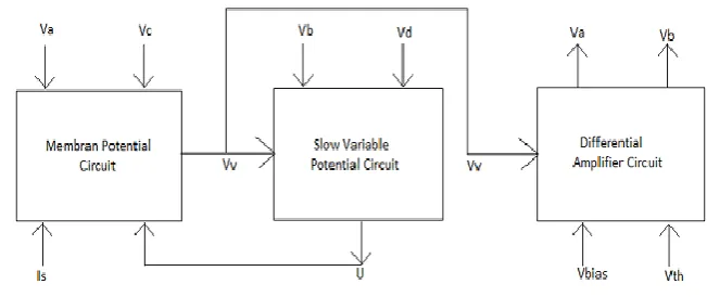
The CMOS based hardware cortical neuron circuit analyzed and simulated in this paper consists of 14
transistors in total [8-10]. This hardware circuit can be further divided into three parts for deeper understanding
of the neuron circuit and it’s various stages responsible for generating the spiking and bursting patterns at the
output.
Fig. 1. Block Diagram of cortical neuron circuit
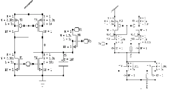
3.1 Membrane Potential Circuit
Fig 2(a) depicts the membrane potential generator circuit [8][9][10][12]. In this circuit supra-threshold input
current Is is provided at the gate terminal of the T1 transistor. Transistors T2 and T3 are arranged in current
mirror formation. The circuit current is generated by transistor T1 which flows to the transistor T2 and
henceforth to transistor T3. The current through transistor T3 at the drain terminal is called Iv and this current is
responsible for generating spikes in the circuit. The leakage current flowing through transistor T4 is Il, whose
value depends on the slow variable potential U generated by transistor T8. The sum of these three currents i.e. Is
, Iv and Il is integrated on the capacitor C1 to generate the membrane potential Vv. Now this increase in
membrane potential Vv, generates a spike. When this spike is detected by the differential amplifier circuit, it
generates a pulse on Va which further switches on transistor T5. Transistor T5 is designed so that the capacitor
C1 gets fully discharged during the pulse Va. The voltage Vc controls the value of membrane potential V which
Fig. 2 Membrane Potential Circuit
3.2 Slow Variable Potential
Fig 2(b) depicts the slow variable potential circuit [8][9][10]. In this circuit transistor T2 and T7 form a current
mirror circuit and the input current is generated by transistor T1. The parameters (W/L ratios) of transistor T7
are set in a manner so that the drain current Ivu of transistor T7 is lower than the drain current Iv of transistor T3.
Also capacitance value of slow variable capacitor C2 is kept higher than that of slow variable potential capacitor
C1. This is done to make sure that the slow variable potential U varies slowly compared to the membrane
potential Vv [20][22]. The slow variable potential U controls the drain current Iu through M6 (and M4, in the
above circuit). The sum of the currents Ivu and Iu is integrated on the slow variable capacitor C2.
After the membrane potential spike, comparator generates another pulse Vb which switches on transistor T8.
Transistor T8 is made narrow so that the capacitor C2 doesn’t get fully discharged during the pulse Vb, rather in
addition to the charge present at the C2, an extra charge is provided to it so as to increase the value of slow
variable potential. This result in increase in leakage current which generates membrane potential and hence
results in slowing down the depolarization of transistor T5 after the spike is generated (called Accommodation
Property).
3.3 Differential Amplifier Circuit
Fig 2(c) depicts the differential amplifier circuit [8-10]. Transistors T9 and T10 work as pull up resistors and are
PMOS transistors. These two transistors form a current mirror configuration. Transistors T11 and T12 are the
NMOS transistors which compare the inputs provided on their gates and generate the Va and Vb pulses which
are always complementary to each other (which is visible in further simulation results). These two transistors
(T11 and T12) perform the differential amplifier operation. Transistors T13 and T14 are NMOS biasing
transistors to control the biasing of the differential amplifier circuit part. Furthermore, an input is provided at the
gate terminal of transistor T11 in form of a constant dc voltage Vth called spike detection threshold voltage of
the potential created at the membrane Vv.
When membrane potential Vv rises above the value of spike detection threshold voltage Vth, then voltage at Vb
decreases and voltage Va increases, resulting in generation of reset signal. Due to delay in transistors used, reset
signal gets delayed and membrane potential increase above Vth to Vdd voltage. Once the reset signal is
received, the value of membrane voltage gets reset to the voltage Vc (whose value is lower than that of Vth).
This completes the reset pulses and Va, Vb return to their resting voltage levels.
The W/L ratios of all the transistors are maintained so as to provide the required delay in the reset circuit.
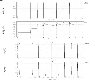
IV. IMPLEMENTATION AND RESULTS
The CMOS based analog circuit of cortical neuron is simulated and analyzed on Tanner EDA tool at 250nm
CMOS technology node [8-10]. The simulated results are shown in Fig 3. The spiking patterns can be varied by
changing the values of voltages Vc, and Vd.
The parameters used for carrying out simulation and analysis of the circuit on Tanner tool are (W/L)M1 = (2.3/1),
(W/L)M2 = (2.3/1), (W/L)M3 = (2.3/1), (W/L)M4 = (1.3/22), (W/L)M5 = (5.3/1), (W/L)M6 = (1. 3/18), (W/L)M7 =
(1.3/14), (W/L)M8 = (1.3/1), (W/L)M9 = (1/3.8), (W/L)M10 = (1.8/1.3), (W/L)M11 = (1/4.3), (W/L)M12 = (1.3/1),
(W/L)M13 = (2.3/3), (W/L)M14 = (2.3/3), Vc= 0.1V Vd= 0V, Vth= 1.7V, Vbias= 0.6V, C1 = 0.1 pf and C2 = 1 pf
[9][10]. The supra-threshold input current Is is taken as astep of 0.1uA [10]. Further parameters are given in
Table 1 below.
Parameter NMOS PMOS
Tox 225.00E-10 225.00E-10
Cox 0.44µF/m2 0.44µF/m2
K 5.34cm2/V-s 1.5925cm2/V-s
Vto 0.622490 V -0.63025V
Kp 6.326640E-05 2.635440E-05
Lambda 0.0 0.0
Nsub 1.066E+16 6.575441E+16
Fig. 5. Simulation Waveforms of the Membrane Potential(Vv), Slow Variable Potential(U),
Pulses Va and Vb
Furthermore, the differential amplifier circuit (block 3 in Fig. 1.) part of the neuron circuit is analyzed in detail.
This is carried out by varying (W/L) ratios of the transistors T9 with respect to T11 and that of T10 with respect
to that of T12 of the differential circuit part of the whole circuit and then simulating the neuron circuit on
Tanner EDA Tool to check and analyze the results. The variation in Va and Vb pulse by changing the (W/L) of
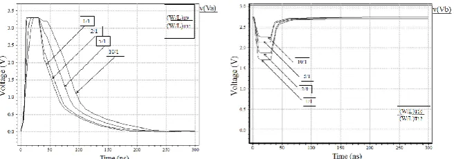
T9 transistor with respect to that of T11 is carried out and the variation of Va pulse is shown in Fig. 6(a)
(changes are more visiblein Va pulse as it is the output taken at transistor T11). There are four different
waveforms, generated by changing the (W/L) ratios of transistors T9 and T11 with respect to each other. The
initial value is taken as (W/L)T9 = 0.3/1.3, (W/L)T11 = 0.3/1.3 and (W/L) ratios of all the other 12 transistors are kept similar as detailed above. After that subsequent ratios are generated by simply multiplying the integer
number with (W/L)T9 and keeping (W/L)T11 same for all the waveforms i.e. the initial condition gives the waveform with 1/1 ratio, then 2/1 ratio is generated by making (W/L)T9 = 0.6/1.3(twice of its initial value), 5/1 ratio is generated by making (W/L)T9 = 1.5/1.3(five times of its initial value), 10/1 ratio is generated by making (W/L)T9 = 3/1.3(ten times of its initial value). The variation in Vb pulse is similar and complementary as compared to Va pulse for the case described above.
On similar lines, the variation in Va and Vb pulse in carried out for transistors T10 and T12 and variation in Vb
pulse is shown Fig. 6(b) (because in this case changes are more visibleon Vb pulse as it is the output taken at
transistor T12). There are four different waveforms, generated by changing the (W/L) ratios of transistors T10
and T12 with respect to each other. The initial value is taken as (W/L)T10 = 1.8/1.3, (W/L)T11 = 1.8/1.3 and (W/L) ratios of all the other 12 transistors are kept similar as detailed above. After that subsequent ratios are
(W/L)T10 = 3.2/1.3(twice of its initial value), 5/1 ratio is generated by making (W/L)T10 = 9/1.3(five times of its initial value), 10/1 ratio is generated by making (W/L)T10 = 18/1.3(ten times of its initial value). The variation in Vb pulse is similar and complementary as compared to Va pulse for the case described above.
Fig. 6. (a)Variations in Va by changing the ratio (W/L)
T9/ (W/L)
T11, (b)
Variations in pulse Vb
by changing ratio (W/L)
T10/ (W/L)
T12V. CONCLUSION
The CMOS based analog circuit of cortical neuron is simulated and analyzed using Tanner EDA tool using
250nm technology file. The spiking patterns generated after simulation are studied and the differential amplifier
part of the circuit is analyzed in further detail. The circuit is analyzed by varying the (W/L) ratios of the T9-T12
transistors and their results are compared for better clarity of the working of the circuit. The analyses result
show that this single circuit can generate varying spiking patterns like the biological cortical neuron. With
variation in parameters (different stimuli in case of biological neuron) the spiking patterns show variations,
hence, by analyzing this circuit we have been able to study how a analog circuit can replicate the behavior of a
biological neuron cell.
REFERENCES
[1.] Richter Z., Janszky J., Gyorgy S., Horvath R., Horvath Z., Doczi T., Seress L., Abraham H.: Characterization of
Neurons in the Cortical White Matter in Human Temporal Lobe Epilepsy. Neuroscience, Vol. 333. (2016) 140–
150
[2.] Joubert A., Belhadj B.: Hardware Spiking Neurons Design: Analog or Digital. IEEE World Congress on
Computational Intelligence, Brisbane Australia (2012)
[3.] Misra J., Saha I.: Artificial Neural Networks in Hardware: A Survey of Two Decades of Progress.
Neurocomputing, Vol. 74. (2010) 239-255
[4.] Tete A.D., Deshmukh A. Y.: Design of Cortical Neuron Circuits with VLSI Design Approach. Int. J. on Soft
Computing Vol. 2. (2011)
[5.] Indeveri G., Barranco B.L., Hamilton T.J., Schaik A.V.: Neuromorphic Silicon Neuron Circuits. Frontiers in
Neuroscience (2011)
[6.] Essera S.K., Merollaa P.A., Arthura J.V., Cassidya A.S.: Convolutional Networks for Fast-Energy Efficient
[7.] Seminaraa L., Pinnaa L., Ibrahima A., Nolia L., Capurrob M., Cavigliaa S., Gastaldoa P., Valle M.: Electronic
Skin: Achievements, Issues and Trends. 2nd International Conference on System-Integrated Intelligence:
Challenges for Product and Production Engineering, Procedia Technology Vol. 15. (2014 ) 549 – 558
[8.] Wijekoon, Jayawan H.B., and Piotr D.: Spiking and Bursting Firing Patterns of a Compact VLSI Cortical
Neuron Circuit. Proceedings of Int. J. Conference on Neural Networks, Orlando Florida USA (2007)
[9.] Wijekoon J.H.B., Dudek P.: VLSI Circuits Implementing Computational Models of Neocortic Circuits. J. of
Neuroscience methods Vol. 210. (2012) 93-109
[10.] Wijekoon J.H.B., Dudek P.: Compact Silicon Neuron Circuit With Spiking And Bursting Behavior. Neural
Networks 21 (2008) 524–534
[11.] De M., Juncheng S., Zonhjua G., Ming Z., Xiaolei Z., Xiaoqiang X., Qi X., Yangjing S., Gang P.: Darwin: A
Neuromorphic Hardware Co-Processor Based on Spiking Neural Networks. J. of Systems Architecture Vol. 77.
(2017) 43–5
[12.] Zhao C., Wysocki B. T., Liu Y., Thiem C. D., Mcdonald N. R., Yi Y.: Spike-Time-Depenent Encoding for
Neuromorphic Processors. ACM J. of Emerging Technologies in Computing Systems, Vol. 12. No. 3. Article
23. (2015)
[13.] Wijekoon J.H.B., Dudek P.:Simple Analogue VLSI Circuit of a Cortical Neuron. 13th IEEE Int. Conference on
Electronics Circuits and Systems (2016)
[14.] Bakhshiev A.V., Gundelakh F.V.: Application the Spiking Neuron Model with Structural Adaptation to
Describe Neuromorphic Systems. Proceedings Computer Science Vol. 103. (2017) 190–197
[15.] Indiveri G.: A Low Power Adaptive Integrate-and-Fire Neuron Circuit. IEEE Int. Symp. Circuits and systems,
Vol. IV. (2003) 820-823
[16.] Petit B.I., Murray A.F.: Synchrony Detection and Amplification by Silicon Neurons with STDP Synapses.
IEEE Transactions on Neural Networks, Vol. 15. (2004) 1296–1304
[17.] Wojtyna R., Talaska T.: Trans-resistance CMOS Neuron for Adaptive Neural Networks Implemented in
Hardware. Bulletin of the Polish Academy of Sciences Technical Sciences, Vol. 54. No. 4. (2006)
[18.] Castaños, Fernando, and Alessio F.: Implementing Robust Neuro-modulation in Neuromorphic
Circuits. Neurocomputing, Vol. 233. (2017) 3-13
[19.] Koickal, Thomas J., Luiz C. G., and Alister H.: A Programmable Spike-Timing Based Circuit Block for
Reconfigurable Neuromorphic Computing. Neurocomputing, Vol. 72 No. 16. (2009) 3609-3616
[20.] Cassidy, Andrew S., Julius G., and Andreas G.A.: Design of Silicon Brains in the Nano-CMOS Era: Spiking
Neurons, Learning Synapses and Neural Architecture Optimization. Neural Networks Vol. 45. (2013) 4-26
[21.] Morabito, Francesco C., Andreas G. Andreou, Elisabetta C.: Neuromorphic Engineering: From Neural Systems
to Brain-like Engineered Systems, Neural Networks Vol. 45. (2013)
[22.] Asai, Tetsuya.: A Neuromorphic CMOS Family and Its Application, International Congress Series, Vol. 1269.
(2004)
[23.] Nazari S., Amiri M., Faez K., Amiri M.: Multiplier-less Digital Implementation of Neuron–Astrocyte Signalling