DEC
STANDARD
160
I.e STD 161, Section , 17-8ep-81 paqe 1
...
LBI-ll BlB SPB::IrlCATltM-Il£SIGH SPBCIFlCATltM
'!'his standard includes the information necessary to
interface to the LSI-ll Bus. Section' il the
specification. It Is a qenerlll, or universal.
specification with no references to Diqital products past or present. It covers the 19811 version o! the LBI-ll BUI. includinq 22 bits of address space and block lIIode tran~ers.
Section 1 is a 'listory or folklore section with references to past Diqital productlll am Is more instructional in nature. It refers to past Dlqltal baekplanes that implell8nted syst!!lllS havinq 16 bits and 18 bits of address spae{o.
100, ORIGIIlATOR
17-Sep-81
tIoc..-nt IdentiUer
DPJ::
sm
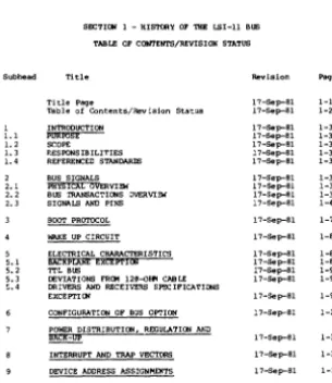
160, Section ~ 17-Sep-81SECTICM III -DESIGN SPECIFtCATION TABU: Ol!' CON'l'tNTS/REVISION STAT!!>
Page 2
Revision P"g"
,
'-'
,.,
U L ''-'
t.6 1.7,
,.,
,.,
'.3
,.,
'.5
Title Page
~ble of Contents/Revision Status
INTR0O\JCTION " " , . , . . .
-RESPOlISIBILITTES HCW
'ro
USE THIS DOCtJoIENT REFEREo!oCED STAlIDAROO CONFORMANCE GLOSSARYBUS SIGNALS PHYSICAL OVERVIEW Bill TRANSACTIONS OVER-VUW SIGNALS !>.Nt> PINS
ELECTRIC},L CHARACTERISTICS OVERVIEW AND O£siGii GOALS THEORETICAL DESIGN CENTERjQ-BUS SPECIFICATIONS
O~t.tS IMPLEMENTATIcti GUIDELINES
PROTOCOL ~/1X.Io'N PROTOCOL
INITIALIZATION
BOOT PRO'rOCOL
DATA AND ADORESS STRUCTURE OVERVIEW BUS MASTERSHIP (t:M:» PROTOCOL
17-Sep-81 17-Sep-Bl 17-Sep-B1 17-5ep-Bl 17-Sep-Bl 17-Sep-Bl 17-Sep-Bl 17-Sep-Bl 17-Sep-Bl 17-Sep-Bl 17-Sep-81 17-Sep-Bl 17-Sep-Bl 17-Sep-Bl 17-Sep-Bl 17-Sep-Bl 17-Sep-Bl 17-Sep-Bl 17-Sep-Bl 17-Sep-Bl 17-Sep-~1 17-Sep-81 17-5ep-Bl 17-Sep-Bl
ENVIRONMENTAL REQUIREMENTS 17-Sep-81
Fl/IItCTIONAL DESCRIPTIONS OF BUS SIGNALS 17-Sep-81
APPEN!:JlX A. Q22-SIS PARITY 17-Sep-Bl
DEC STD 16". Section (! 17-Sep-81 Page J
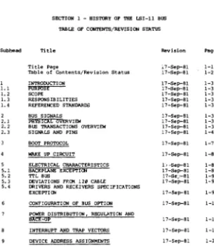
SECTICII' I - HISTORY OF THE LSI-ll BUS
TABLE OP CCll'TENTSjREVISION STATUS
Revision
....
Title
'''.
l7-Sep-81 HTable of Contents/Revision StattlS 17-Sep-81 H
,
INTRODUCTION l7-Sep-BI HU ~ 17-Sep-81 H
U l7-Sep-Bl H
U P.£SPONSIBILI'!'IES 17-Sep-81 H
L'
REFERENCED STANDAAIS 17-Sep-Bl,-,
2 BUS SIGNALS 17-Sep-Bl
,-,
2.' ~VI!W 17-Sep-Bl H
2.2 BUS TRANSACTIONS OVERVIEW 17-Sep-Bl H
2.'
SIGNALS .>.NO PINS 17-Sep-Bl H~ 17-Sep-Bl
WAKE UP CIRCUIT 17-Sep-Bl
,
ELECTRICAL CaARACTERISTICS 17-Sep-81 '-8,.,
IiAtkpWE eXCEpt 100 17-Sep-Bl 1-8>.2 TTL BUS 17-Sep-Bl 1-9
,.,
DEVIATIONS FRCM 1211-O~ CABLE 17-Sep-BI 1-9!:.4 DRIVERS AND RECEI'v~ SPECIFlCAT!~S
EXCEPTItti 17-Sep-81
CONFIGURATION OF BUS OPTION 17-Sep-81
POWER DISTRIBUTION. REGULATION AND
BAcR=tJp 17-Sep-BI
INTERRUPT AND TRAP VECTORS 17-Sep-Bl
[image:5.207.23.176.39.215.2]DEC STD 161. Section il 17-5ep-81 P;:oqe 4
TABU: OF CtwrEH'l'S/REVISION STATUS (Conc'dj
Figure Title
l'Iinim~ Configllf<ltions
Illteme:liate Configur<'lcions
Maxim~ Configurations
Pt.wer-Up/Power-Down Timing
IlMA R'lquest/Grant Timing
DATI BII~ Cycle Th,lng
DATO or
""",.
,~ Cycle Timing DATIO Bus Cycle Tim~ngDA'IlH Bus Cycl" Timing
DATBO Bus Cycle Timing
Intern,pt l'rallsaction Timing
Sunmary of Signal Line Functions
[51-11 Bus Si~nals and Pin SLlllmary
SUO'IIIary of ~ta 'hansfer Bus Cycles
Revision
'''.
17-Sep-81
17-Sep-81
17-Sep-81
l7-Sep-Sl
17-Sep-Bl
17-Sep-Bl
17-Sep-&1
l',-Sep-Bl
17-Sep-Bl
17-Sep-81
17-Sep-81
Revision p;:oqe
17-Sep-81
17-Sep-81
IZC STD 161, Section II l7-Sep-fll P8/Je 5
~
The orig_> ,1 baekphne to implement the ISI-ll Bus was designed to acCOllllllOdate Digital's quad and dual height lKIdules. I t became known as the ·O-8us· to refl~t the quad board fonD. factor. Both ISI-ll bus and Q-BUS are Digital t:adelllarks, but are not registered tradelllarks. several ~us architecture features of the LSI-ll Bus are protectlll! by claillS in Digital Unibus patent nllll:bers 3,7111,324 and 3,815,1199. SOllIe publ1catlons m"y also use the term SUB-tlMIBIIS, although this is not reeOlllllended.
MIen the tsI-ll Bus was expanded to provide 22 address 11nes, tile terms Q22-Bu$ and extended LS!-ll Bus were adopted to specify backplanes that bus the four additional lines.
The ISI-ll BUS Is defined by this standard as the interconnection macH,.. for LSI-ll system components. By adhering to specifications included in this standard, the designer can correctly design and configure system hardware that will be cOll\patlble with othl"r LSI-U system components designed to the sa!!!e standard. Each Digital option or system canponenl that is designed to connect to the LSI-ll Bus, or a subset of LSI-ll Bus functiens, must comply with this standard.
This section contains complete specifications for the ISI-ll Bus, including quantitative descriptions of signals, functional descriptions of signals, protocol, elec:trical and transmission line characteristics, transceiver specifications, tilQing constraint:! and configuration restrictions.
1.3 RESI'aEIBILITIES
This standard is the result of efforts by the Q-8us Task Parce, Which ~ representative of the des!qn cOIIIIIunit} of engineers frOli produet _ne and central engineering organizations. Accountability and responsibility for maintain.nee of this standard resides with one person. 'nIat person is desiqnated responsible 8I"gineer and Ilia or her name will appear as the latest ociqinator on the title paqe of this standard. It is that person's responsibility to convene the task force to review aOO approvOil any ECQ's to this standard, to siqn ECO's, and to transfe~ accountability via 8:0 to upd"te "<.rt.hor history.
A list of past and current O-Bus Task Force lIIl!1IIbers is lIaintained on file by Diqital Standards IodlQinistration, ML3-2/E56, tn'N= 223-9475.
DEC STD 160, Section 0 17-Sep-61 Page 6
1. 4 H(M TO USE TIllS IXlCtMENT
First, USe the Table of Contents to find specific items of interest, such as DATI Proto(;ol or Bus Mastership Protocol, or Electrical Characteristics.
Sec.,nd, I<now how thi.s document is organl-zed. Section ~ Is the true and current specification of the bus, and all designs released ~fter the release date of this specification shall conform to it. It is organized to provide '" series of "verviews for first time us"rs, f,,!lowed by specificati"ns. Section 1 i,; a history of previoi.lS v"rsions of the bus.
Conv .. ntio"s used in the protocol section follow the electrical section a"" . recetie the protocol section.
The proto,",ol descriptions are presented with overviews, followed by specification format where possible, otherwise by just sP<!'Cifications, as follows,
Power Up/Down Protocol (specification) Ini::ialization (specification) Boot Protocol (specification) Data/Address Structure (specIfication) o..f1nition of I/O Page (specification) Inter~Uj:.t Structure (ovetview) Bus Mastership (OMA) Protocol (specification)
Data Transfer Prtltocol (speciiication) "efresh Protocol (spacificlltion) Interrupt Protocol (specification) BEVENT and BBOK Protocol (specification) HALT Protocol (specificlOtion)
Third, classify your needs frO'll this dO<'llIIlent.
If you "'0. no. ... to t,le Q-Bus, you will benefit most by reading the document complet .. ly. It will take less than a" hour, if r~~e~'~:tt. relOd it ,ithollt stlllllbling over points of technic.al
b. If you are deSigning a Q-Bus option, yael may w,mt to go directly to the electrical charOicteristics lind protocol aescrlpticns of interest to you.
c. If YOll are involvdl in older Digital systems, the history of the [51 Sus in Section 1 may be ;)f more interest.
DEC STC Ifill. Section II
DEC STD 11'13. (proposed)
DEC 51'0 158 (proposed)
17-Sep-81 Page 7
DeSign Review Process
ModuJ.e ~nufacturinq SUndard
Environmental Standard For Computers and perIpherals
~;;d;~~~fi~:f!~ li:Gi;!~l,!;y
(EMC)
Ac Power Line Stand"rd
Unibus Specification
Signal Integrity
All new desig,1s must be reviewed in IOccordance with DEC STO 11'1'17, Design Review Process. I t is the responsibility of those persons p1Irtlclp...tlng In the design review of a new product that connects to the LSI-ll Bus to aSSUre that the design confo!'1lls to the requirl!lrl>lnts stated in this specification.
Async:hronous - !ndic<ltes that an event occurs withou~ any fixed or constant time relationship with respect to bus Signals.
BackplMe - 'l1le physical lIIOuntinq blocks into which modules are inserted; bus $ign<lls are connected on the revers .. side by wire or etCh.
Bus Se;lDent - Pertion of the Q-8us system bet_en and including tWO te!'1llinators. A bus segment consists of a temination. a l:<II-ohlll transmission path (cable) with options containing drivers and receivers attached to it, ar.d ,-,nother terminaton in that order.
DEC STD 160, Section 0 l7-Sep-8l Paqe 8
Cross-talk - Injection of a voltage or current spike into a signal lIne due to capacitive or inductive coupling frOOl adjacent signal lines.
Daisy (hain -A bus sign<l1 that is broken at each module slot, which may be te[l!linated or passed along by the insertion of a module with circuitry.
E'll LSI-ll/23 - A family of progralllllable data processors. microprocessor chip set consi:;ts of the following part'H
57-SSSSS-SI DAT/C'I'L 21-15542-111 I9!:U 57-SSSIII-U FP
Far End -The far end of the bus is the last bus interface slot (the near end is the first).
Finger - The point of contact between a signal on a module or a cable and the same signal on a backplane~ also called a pin contact, con.'Jector, or connection point.
Interrupt Fielding Proees.$Or - Usually considered as part of the processor or processor module, this control loqic arbitrates asynchronous interrupts from devices on the bus to determine which aWlce has a higher priority. Once the priority is established, tile processor ~knowledges the interrl1pt.
Logic RP.ference -Retum path or common p::.wec supply output for a logical c'.<:erence voltage (i.e. with 'M'L a logic "I" might be 3.4 V with r .. ~t>eCt to logic reference). Sometimes referred to as 9.-ound.
lSI-ll - A family of progralllnable data processors based on tha 1$1-11 microprocessor chip set, which includes the following parts,
21-15579-1111 OAT 23-1102C4-110 CTL 23-1101B5-&0 MICRctI 23-1111285-1111 MICRCII! 23-1111385-116 filleR""
Master -The device, module or option that is currently controlling bus transactions. There can only be one bus lMster at a time.
DEC STD 169, Section
a
17-Sep-81 Page 9OOT, Online Oebugqing Technique (1ilI1t Mode) - Some processors feature a console cGmlllunication mode for debugging iIInd star!:ing programs from the Halt state, which is called ODT.
PC, Pcoqum Counter - A proce"sor ragister that generally contains the address (memory location) of the next instruction to be executed.
ps, PSW, ~ocessor Status Word -A processor ragister that contains data relevant to the status of the processor iIInd the operation most recently completed; the dillta indicates what interrupt levels will be acknowledged and whillt sorne of the results of the most recently completed operation were.
Q-Bus - Any of a .,=:>up of backphne and cable systems th"t carry the Q-Bus sign"ls, including 18 lines for address delimitation.
Q22 Bus - Any of a group of backplane and cable systems that impl'!ment the Q-Bus signals and are capable of handling 22 lines for "ddr"ss deli",itation.
Signal Skew - The difference in propagation delay between any tWO devices. one being at maximum propagation delay and the oth .. r being at minimum propagation delay.
Slave - A bus device that can be addressed by, and participate in bus transactions with a bus master. rt has the subordinate r<>le in a data transfer.
Slot -One of several locations into which a modular interface with the bus may be physically inserted.
St"ck -An area of memory reserved for storing working proqram data. IJnd~r control of a processor register called the st"'ck pointer, data is referred to as being p.lSCled onto and popped off of the SUck, in a hst in, first out sequence.
State IJ -In devices whose logic proceeds through a series of .'ltates after power up, the initial, ready to begin work, state is often referred to as state ~.
Stut> - A connection to a bus line that does not form part of the continuous conductor from near end to far end.
DEC STD 16.1, Section It 17-Sep-81 Page Iii
An LSI-l1 computer" system Is basically a controlling pr"ocessor, memory ard I/O (input/output) devices. These devices ar"e generally cunstr"ucted on pt"inted circuit boards, sometimes called modules, Ionich connect to the bus viii finger"s.
Mechanical fonn factor/dimensions of dual and quad Digit"l modules can
be fourd in DEC STD.il3i1, Module Manufacturing Standard. The fingers of the module plug ll'lto connectors Whose Pll'lS become the LSI-ll Bus
signal lines. These lin .. s may be connected "1a etch or wir"es and these Wires or etch on the back of the block become the backplane. IJp to three b~kp1anes may be connected by cables totaling a maximllll of 16 feet. A total of 42 signal lines are used in the ISI-ll Bus. The signal lines are functionally divided as listed in Table 1.
Table 1. SUIIIIlary of Si'1nal Line F'..mct1ons
Quantity II : Bus S1'1nal Mnealonic
---+,
- - - 1 ' r
I Data/Address Lines I BrAL<lS,fle>
I I
I Memory Parity/Address Lines I BfilU.<17,16>
I I
I Address Lines I B!liU.<21:IB>
I
I Addres15 aoo Data Transfer I BSYNC, BOlN, BOOUT,
I Control Lines I !Io/'l'BT, BaS7, BRPLY
I I
I [)ir<Jct Memory Access IJIIA Control I BtMR, BDlG, BSACR
I Lir • .es I
I I
I Interrupt Control Lines I BIRQ4, BIRQS, BIRQ6,
I I BIR07, BIAK
I I
I System Control Li .. es I BPOR, BOCOK, BUilT,
I I BAALT, BREF, BEW'I'
I I
,1,11 LSI-ll Bus signals are asserted low /'Ind negated high, except BPOK and BOCOK, which ilIre asserted high and negated low to indicate an event such as impending loss of pow@r.
[image:12.207.23.178.19.243.2]DEC STD 160. Section 0 17-S.p-8\ Page 11
LSI-II Bus signals. with the exception of IMA grant anI'! interrupt acltnowle9ge signals, are .bi-directional. This mean:; they can be Clriven or [ecen,ed at any pomt along the signal Ilne. Iotten Clriven, bi-directional signals travd in two djrections; frOl!! the driver to the near end terminator, and from the driver to the far end ~~rminator. The exceptions are BlAKO L, SIAI(I L. SrMGO L, and arMG!
BIAKI r (Interrupt IIckn" ... ledge) is received by an LSI-ll Bus device ~,n 'One pin and conditionally jdependirx; on whether or not the device has ohe highest priority inter~upt pervling) re-transmitted out within 500 ns on a different pin as BIAJ(O L to the next device on" the bus.
Bus wiring connects BIAKO L as output from one device to BIAKI L as input ta the next device on the bus. BrMGI L and BrMGO L form a similar priority daisy Chain far Bus l'Iastflrshlp Grant.
Devices connect to all Q-Bus lines via high impedance receivers and gated, high current, open-collector drivers.
There are four basic kinds of transactions t.IJ.at can take place ov"r the bus;
a. Power up/down signal sequencing.
b. TranSfer of buS mastership from bus master. c. Transf .. r of data betwefln a bus master and a slave. d. Interrupts to the interrupt fielding processor.
These basic transa.::tians and their variations o.::cur within the constraints of protocols Clefined in the protocol section of this standard.
2.2.1 <'ower Up/Down Overview
Idlen IX>wer is first applied, the BPOJ( H, BOCOI( Hand BINIT L Signals initialize devices on the bus and cause the controlling processor to aSSUme control (mastership) of the bus. 1he controlling processor may then execute sane boot program or other power "'p option.
2.2. 2 Tr"ln",'e~ of Bus Mastership
DEC STD _ .... , Section" 17-5ep-8l Page 12
Data transfers occur asynchronously ;oithin a master/slave relationship under- a strict protocol defined in this standard (sllbhe"cl 4.4). The controlling processor is generally the default bus master. It will relinquish bus mastership to any requesting device (sometimes referred to as a direct memory acceSs or !PIA device) when it is not curr"ntly US1"'3 the bus. My device that contains the appropriate circuiny may become the bus master and control dllta transfers over the bu.s to or from any slave device.
aecause bus cycle completion by the bus master requires response from the slave device, each bus master must include a time out errOr circuit that will abort the bus cycle if the slave device does not respond within the required U microseconds. Masters generally allow 12 microseconds.
2.2.4 Interrupts
Interrupts to the interrupt fielding processor from any device on the bus follow a ll!lique protocol. When a device wishes to interrlJpt the processor, it asserts a request 1 ine. When the processor acknowledges the interrupt, the device places an dddress (called a vector) on the bus and the processor redds the conten"s of thdt dddress locdtion and the ~ollowing one to obtain a new PC and PSW.
The processor then ex"""tes the interrupt routine starting at the nf'W PC. When the task is completed, the last instruction, RTI or RTT, restores the old PC and PSW from the stack. The processor then starts executing the instructions located at the address of the old PC (where it was inte~rupted). See processor handbooks for more detail on interrupt and PS'';. InterruptS are prio[itized and "re deseribM in detail in subhe"d 4.5.4.
2.3 SIGNALS AND PUIS (Quantitative and Deseriptive Dlrerview)
rEC S1'O 161, Section 1 1?-5ep-8l paqe 13
ISl-ll Bus Signals and Pin S~ty
:~~si:
Functional Category1
Digital's Nomencbture (name)--1-,
---~,f---
(Pin)) Data/Address I BOALS, BMLl, BML2, SC.o,LJ ••• BMLIS
I I AU2 AV2 BE2 BF2 ••••• BV2
I I
2 ) Memory Parity Control/ I BOALI6, BDALI?
I Etror Address I ACI ADI
1 I
I Address I BMLI8, BML19, BI».L21, BI».L21
I I OCl BOI BEl BFl
1 I
I Address and D:lta I BOOOT, BRPLY. aOIN, BSmC, BW'IBT, SSS7
I Control I AE2 AF2 AH2 AJ2 AK2 AP2
I 1
6 I Device Interrupt I BIRO?, BIRQ6, BIRQS, BIRQ4, BlAKe, BIl!.KI
I Control I BPI ASl AAI AL2 AN2 11M2
I 1
I [MA Control I BrJIlR, BSACK, BrMGO. SrHGI I I ANI BNI AS2 AR2
I I
I System Control I BHALT, BREF, BEVNT, IUNIT, BOCOK, BPOK
I I API ARl BRI AT2 BAl BBl
I I
I S SPARES I AEI, ARI, BBl, AFI
I I (Slot 1 only, SRW @ AFI)
I I
I 1'1 SPARES I AKI , ALl, SKl , BLI (pai:"s connected)
I 1
2 I P SPARES I AUI, BUI
I I
I +l2B (battetyl I ASl, SSI
I 1
I .. SB (battery) I AVI
I I
I .. S Vdc I AA2, BA2. BV!
I I
I .. 12 Vdc I A02, B02
I I
2 I -12 Vd:: I AS2, BS2
I I
I GND I AC2. },J1, HU, ATI, &,2, B,n. SHI, BTl
DEC S'l'D 1611, Seetion H 17-5ep-81 Page 14
ELECTRICAl. ClIARACTERISTICS
'!'he Q-Bus is designed to be the interconnect mediUIII for df'Vices that consist of Slndl, LSI-based PDP-ll computirog systems. Some of the design goals are;
a. That the customer's systems be expaondable and upqradeable (i.e. not a b>unded system)
b. That the bus will have well-controlled characteristics and clearly defined limits consistent with the term "small computer system".
c. '!hat the mmb,oor of hus signals be as small as possible, ..tIile "Onsistent with PDP-ll functionality.
With these goals in mind, and a knolo/ledge of available interconnection and transmission technolo::ry, the de.:.igners developed the Q-bus.
3.2 THEtRETlCAL DESIGN CbTER/Q-BUS SPECIFlCATIClolS
3.2.1 Sackplanes
3.2.1.1 Maxim . . Nuaber of Backplane. -A sY!ltem can nave either one, two, or three backplanes. Bus signals run frail the near end of the first backplane to the far end of the last backplane.
3.2.1.2 Impedance of Wire or Etch - n,e Characteristic impedance of a backplane Signal 1 ine, wi th all other signal 1 ines and log ic references tied together, must be 12i1 01Ds, .! lil\.
3.2.1.3 Maxim,. Resistance of II Signal Line - A signal line (wire or etch) must have a de resistan.-e of less than iI.l ohm per signal line.
Ole sm lSI. Section I hga lS
Pigor!!! 1. lIinl_ configurations
Pigura 2. Intemadiata Configurations
DEC S'm 16!!. section •
PROCESSOR
f--B:;'::-~a~;1 :~~~----I
---11---.---,
NOTES:
1. TWO CABLES (MAX.l4.aa .. (l6fHIMAX.1
TOTAL LENGTH.
2. 20 DC UNIT I...CIADS
T01'ALOMXJ
fag. 16
1'191.11'.]. ...xi . . . Conf19l.1ratlonlJ .e:.;,::;
DEC
sm
168, Section" 17-Sep-Sl Page 173.2.2 InterCtlnnect a,bles
3.2.2.1 Impedance of Cable
With a two or moee backplane system, an interconnect cable c ... n be used to ~us the backplanes together. '!'his cable must h,lVe II ch"ractee~ lStlc impedance of 120 ohms, .:!::
2n.
3.2.2.2 Jllalliml.llll. Length of Cable - In a two backplane syStem, the interconnect cable (or cable set) must be between 2 and 16 feet long.
In a three backplane system, one of the two interconnect cables must be betwe!<n 2 and 6 feet long: the other interconnect cable must be at least 4 feet long, but not more than 18 feet long.
3.2.2.3 Maxill" . . Crosstalk - With a constant voltage ot 5 volts on a given 5igO<'l1 line (victim line), and " S ru; rise/hll time pulse applied to "ll other sign"l lines simultaneously, the crosstalk on the victim line must be less than 5' of the 5 volts (or .25 volt). '!'his must be true for both near and far ends of the cable.
3.2.3.1 Hallillll.llll. Conu,o;t Resist ... nce - A contact p:lint (such as cable
to cable he<'lder or module-·to-backplane) must have a do; r .. sistance of less than 11.112 ohm.
3.2.4 Return Path (or Logic Reference [..ine)
DEC STD 169. Section I 17-Sep-Bl paqe 18
3.2.4.2 Signal Path Routing' - Logic reference, or the retum path for bus receivers must be part of the bus signal di"trib..,tion.
Common system, or power reference, i,!round) must be .. outed a minimum of th .. e.. 'nches outside of and away from the bus distribution path.
3.2.5 Bus Drive"" ... nd Receivers
3.2.5.: Lell9th of Etch from. Drive"jReceiver to finger - from the module fillger (module contact point) to the output pin of a driver 0" the input pin of a receiver, the length of etch must be less than two inches. Drivers and receivers are conSidered part of the bus even though they are located on the modulp
3.2.5.2 Driver and Receiver Power and Reference Separation -Drivers and Receivers shOUld have adequate (511 mil nomin"l, 3e: mil minimUII) and separate power and reference etch. Power and logic reference paths must be direct from finger to IC (no tap offs are <:llowed, except at a finger).
3.2.5.3 Operatill9 Temperature 10nge for Drivers and Receivers -Electrical specifi:=ations for drivers a!Xl receivers must be guaranteed between temperatlJres of e:' C and 7e:' C.
3.2.5.4 Ope.r ... ting Supply VOltaqe Rallge for Drivers and !teeeiver" -Power supply voltage for a driver or receiver can vary between 4.75 volts and 5.25 volts dc wltoolJt violating the specificat"ons in this section.
3.2.5.5 Driver and Receiver Decoul=,ing -Drivers and receivers must
tee STO 16', Section " 17-5ep-Sl
3.2.5.6 Receiver Input Thresholds
-~:~~ -~:~~i!:ut Voltage (VIa) Vee = 5.9 v, .! 5'
Future designs should try to conform to the B641-2 specification for improved noise inmunity.
Paqe 19
3.2..5.7 Receiver Propagation Dl!llay - Propllgation delay frOlll the input of the receiver to the output of the receiver must not be greater than 35 ns. This value should be lII .... sured from the receiver input threshold voltage of 1.7 V, to an output voltage of 1.5 V. An input with a 10 ns rise/faU time with V between 9.B V and 2.6 v must be used for the me<'lsur_ent. Loading of the output will be 399 ollns to +S V and 1.6 kilohms to logic reference, with a capllcitance of 56 pF to logic reference.
3.2.5.8 Receiver Skew -Any two receivers will have a m<'lXillu" skew between them of 25 ns.
3.2.5.9 Receiver Noise :r..lmity - The current 0 Bus receivers do not have a noise rejection specification. The followinq specification Is recOllmended for new receiver designs:
\ Pulse Width (M) Transition Tillie
3.2. ns rise/fall
2.4 ns rise/faU
3.2. ns fall/rise
OEC
sm
101, S£::::tion I 17-Sep-81 Page 21With a 10<!Od circuit of 1.2 koil'lhms and 15 pF to ground, isvlated. by a lN31J64 diode from 211 ohms to +5 Vdc in series with three lN3064 diodes to ground. See the following figure and the 8641-2 specification.
3.2.5.10 Rec:e1ver Input Capac;:itanee - A b<ls receiver can have a maximo..!! input capacitance of 10 pF.
3.2.5.11 Receiver Leakage Current - With Vec between e.0 and 5.25 V dc, the maximo..!! receiver leakage current is as follo!olS:
High Level 80 ua @ 3.8 V dc Low Level -11 ua @ 11.4 V de
3.2.5.12 Driver Po_l" Down Conditiona -During power down of a "US drivel", While it's asserting a bus signal, the driver must ne.;rate that signal a.l<l. not glitch or assert the signal while power is off or during Fl>wer down. Also, when a bus drive, is not asserting a sign"l while powering down, it must not glitch or assert the signal.
3.2.5.13 Driver Output Voltages
Low £.evel output Voltage (VOL) - a.8 V IMxillll.lll @
High Level Output Voltage - It:> high level output voltage Is specified because bus drivers have open collector outp.lts and the specific voltage will depend on bus loading and bus termin"tors.
3.2.5.14 Driver P!:opaqation Delay - Propagation delay frOll! driver inp.lt to driver output, or frem enable to driver output, with an input between 0.0 V and 3.e V, a 11 ns rise/fall tillie, and with 91 ohms to +5.1 V and 2ee olms to loqic reference, must not exceed 25 ns maximUII
DEC S'tD 161. Section 1 17-Sep...81 paqe 21
3.2.5.15 Driver Skew _ a receiver,
between two b..s drive,s, one at maKim<8 propagation daley and other at minimum, must n"t exe:eed 25 ns maximum.
3.2.5.16 Driver Rise ;,ond h l l 1'1_s -Rise and f<oU times 0.0: drivers shall not be less than;
l~ nS: ·",itn 15 pF to logic: referene: .. 25 ns: with 33'" pF to logic reference
3.2.5.17 Driver OUtput capacitance iIlaximUID input cllpacitane:e of l~ pF.
3.2.5.18 Driver t.e.kage Current - Wil:n Vce: between 11.0 V and 5.25 V de: the ;nllximUIII driller leaitag<> c:urrent is as fo110 .. s:
High Level 2S cu. '(I 3.8 v dc
Lo .. Level -l~ Uil Ii! ~.4 V de:
3.2.6 Bus lDading
3.2.6.1 I); ~it !DAd - A de: unit load is defined as 2111~ IlIA, ~ruch is related to the amount of dc leakage e:urrent th .. t a bClS element presents to a buS signal line that is hign (undr;" .. n).
3.2.6.2 AI; !mit !Dad -An Ole ...,it IOlld is defined as 9.35 .,Y, whie:h 1S related to the impedance that a bus element pre!lents to a bus Signal line (due to backplane wiring. pC etch runs, receiver input loading and driller "utput l,,"ding).
DEC STD 1611, Section II 17-Sep-81
3.2.6.4 Maxi . . . Bus
.c
(hit Lo.:lds - Total ac loading allowed in a single backplane system is 45 ac unit loads with 120-ohAI terminators.Total ac loading allowed in a ",,,ltipie backplane system is 22 ac unit l:)ads per backplane.
Refer to document retrieval doc,..ents foe dilta published about ilC and dc loads. values were determined using these doco.nents.
a. Capacitance must be distributed as e'lenly as possible along the bus. Lumped cap,lcit<lnce along a transmission line "'ill caUSe reflections and cause timing relationships to be violate<l.. To insure tnat a bus will be glitch-free, sOltle "nalysis shOuld be done to insure tne proper placement of devices on the bus. ene soch analysis program is PAULI .mich can ~e run by Field Service.
b. AI:: loadS must also be distributed among rhe si"nal lines. l'hat is no single signal line Should have <fIore then a 3 to I difference in ilC loads presant 0;1 the bus to anot~e[ signal line.
Bus Tee-inators - TeraiMting Resistor val\MS
:::~~tor values ttlat meet the following Thevinin equivaler:~ should be
1211 !: 5\ to 3.4V
241:1 !: 5% to 3.4V
me
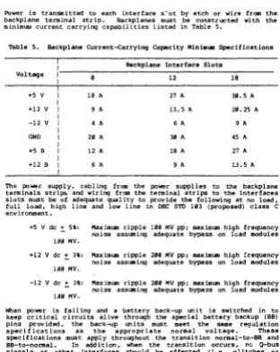
STD 16.. Section • 11-8ep-Sl Page 233.2.9 Power railure Control Slqnals
3.2.9.1 Shorting Element - Siqna1 line BPOk K and BOCOk H are qenerated by the p:.wer supply control logic. \IIhen these slqnals (or a bus siqnalJ are neqated. they lIhould be shorted to logic reference, aceortJirYil to De: STD 186. A pgwer SUv.lly reference other thaO"l 1091c reference, or chassis (earth reference) should never be used.
3.2.9.2 Glitcb Rejection - Devices that lIIonitor BPOK H to perform sollie operation should provide some type of qlitch rejection upon receipt of BOCOK K. 1'IIese devices should use a 1II1n1ll .... of qlitch rejection. as described in paraqcaph 3.2.5.9.
3.3 o-eUS DtPLDIDITATICII GUIIJIUns
Guidelines presented in this section pcovide information for desiqnirYil
Q-Bus system from the electrical viewp:lint. The information Is derived frOli the ~ifications mentioned in subhead 3.2.
3.3.1 Backplanes
3.3.1.1 Length of Btcb or Wire - Wire or etch for a Si9Ml line on each backplane can be a IIlaxilll ... of 8 Inches in a multiple backplane system.
In a system wIth only a sinqle baekplane. the wire or etch ler19th can be a lIIilXialUIII of 14 inches.
3.3.1.2 Connection Points - In a sinqle backplane systea.. there can be 18 connection points (receiver/drIver pair. cable conduetor or teminator) to any bus siqnlll line.
A two backplane system can have up to 12 connection p:.ints in each backplane.
Each backplane in a three backplane systell. can have ,iii to 9 egnnection points.
tEe STD 168. Section II 17-Sep-81 Page <:4
3-.-3.2 Interconnect Cables
3.3.2.1 Allowable cables - Cables that can be used for backplane interconnection ",re the scvllA and BCVUE.
3.3.2.2 Signal Routing In cables -To better con~rol the im~dance and crosstalk of a cable. ~:'" logic reference sho"ld be inter-waved "ith signal lines.
Below is a list of the rcs that can be used ':0 drive and re<:eive bus signals.
_ _ Type"---_""_._-+_Ci.:..,i_td POirt No.
OOC S'l'D 160, Section" 17-5ep-81 Page 25
3.3.3.1 -The driver must not be USed to drive data/address, BBS7, or
W'l'BT linlls onto the bus.
3.3.3.2 -During a rMA request/grant (Figure 5), if the driver is used
for RPLY then the'" ns min1111'- specified fran the negation of RPLY to the negation of Sl!.Ck must be ch ... nged to 1" ns min.
3.3.3.3 -During a DATI or CUt.TO (Figures 6 and 7), when the drivo:.r is
U3ed to drive SYNC, the reh.tionship for the negation of SYNC to the assertion of the next SYNC should be chan,red from 2"'" nS min. to 21lJ ns min. Also, if the ::lriver is used ~" drIve RPLY, the specification for the negation of RPLY to the asserL.on of the n .. :oc:t SYNC should b ..
changed from 38'" ns min. to 31lJ ns min.
In addition, during a DA1'O, i f the driver is used to drive DOUT, the relationship for the l'L'"gation of DOUT to t.;e negation of SYNC must be changed from 175 ns min. to 185 ns lIIin. "nd the relationship for the negation of DOtII' to the rele...St! of the data lines or WTST ml$t be changed from 188 ns min. to lUJ ns min.
3.3.3.4 -For tl).e DATIO caSEI (Figure B), the 0.\1'0 portion of the transfer must follow the s=e restrictions described in the above paragraphs that describ .. 0.\'I'O timing relationships.
During the Cil.TI portion of the transfer when the driver is used for
RPLY, the relationship for the negation of RPLY to the assertion of DOUT must be changed from 2"'" ns min. to 2U1 ns min.
3.3.3.5 - A MnH transaction has the same changes a$ the n.\TI tr ... nsaction and if' addition, when the driver is used fur IIPL't, the relationship for the negation of RPLY to the assertion of DIN must be changed from IS'" ns min. to 1611 ns min. and the relationship of the assertion of !!.PLy to the negation of DIN, when the driver is used to
drive DIN, must be changed frOID 2119 nS min. to 2111 ns min.
3.3.3.6 - A ~mo transaction has the same changes as t'le n.\'I'O tr""nsaction an::! in addition, when the driver is lIsed for IIft't, the relationship for the negation of !!.PLy to the assertion of DOUT must be changed from 15" ns min. to 168 ns min. and the relationship of the assertion of RPLY to the negation of DOUT, when the driver is used to
drive DOUT, must be changed from lSi! ns ... iil. to 1611 ns min.
3.3.3.7 -During an interrupt transaction (Figure III if RPL't is driven with that driver, the relationship for the negation of RPLY to the negation of the vector mUllt be changed from II ns min. to 111 ns lIlin.
DEC $TO 161. ~ti<:m e 17-Sep-81
3.3.3.8 - In addition, caution must be
parity in Appendix A of this standard.
3.3.4 Allowable Terminating Resistors
Page 26
implementing the
In <l single backplane system for a maxim\JIII of 21 ac or dc loads,
including b~kplane, the near end ten<> nation ;'teed only be '" 331--ohm pull-up (to +5 V) and 6Sa-ohm resistor to logic reference. No far .,nd
termination is needed for or sm",ll systems.
t£C STt> 168, Section Ii 17-Se~8l paqe 27
Ttu:oughout the followhg protocol specifications, bus signals are referred to in several different ways,
a. In g .. n .. ral discussions wher .. timing, polarity, and physical location are ur.important, the base sign"l nam .. witllQut any prefixes or suffixes is used. for example:
Most signals on the backplane etch are ass .. rtO!d low. and referred to with a prefix character B. and a SUffix (space) L.
For example'
BSYNC L, BW'IBT L, BBS7 L, BML<17: II> L
BPOK H and BOCOK Hare as;3erted high.
Receivers and drivers are considered part of the hus. Signal inputs to dr~-/ers are referred to with a prefix character T
for transmit. For .. xample:
TSYNC, n.'TaT. 'IBS7, TDAL<17:IIII>
Sio;nal outputs of rec~iv .. rs are referred to with a prefix character R for received. For example:
RSYNC, II<i~T. RB:S7, ~L<17:1I11>
Wh .. never timing is important, c and d above are used to reference timing to a receiver output or driver input. For IIxample. aftllr re<::eipt of the negation of RDIN, the slave neqates its TRPLY '" ns minillllml, 80IJI ns maxim ... ). It must "aintain data valid on its TDA.L lines until II ns minimum after negation of RDIN and must negate iU TDA.f.. lines 198 noS maxilluD after negation of its TI'IPLY.
4.1 POiER UP(O(:tI'N PROTO:OL
Refer to the Timing Dia<;1ral! in Figure 4.
4.1.1 Power Up
DEC ~ 16', Section' '17-se~l Page 28
2. '!'he processor asserts BDiIT [. aft.er raceivi~ nominal po_r and negates BIMIT [. II nsee 1II1nillll"" after the assertion of BOCOX H.
J. Pbw.r S\lPPly logic M9ates BPOK II during power up and a _ r t s SPOK H 71 IllS minlml.lll after the assertion of BOCOK II>. If
power does not rftlaln stable for 78 ma, BOCOK II will be n"",ated, therefore, d ... ,,1ces should suspend critical actions unt.il BPOK B is asserted. 'ItIe assertion of BPOK II will cause a processor interrupt.
4. BPOK II lIust remain aasen.ed for a lIIinim_ of J IllS. BOCCK II
must remair. asserted 4 lUI miniml& after the nl!l)ation of BPO':
H.
Plq:uce 4. Power-Up/PoVer-Dowl Tiaing
1. If the ac voltaqe to a power supply drops below 7S, of the n_lllal voltage for one full line cycle (IS - 24 ms), BPO': R is n"",at.1Id by the power aupply. Qlce BPO': R is naqated the entire pover down sequence DUllt be cClllplet.ed.
DEC STD 1611. Section Il Paqe 29
2. Processor software should execute a RESET Instruction 3 mS miniMLIII after the negation of BPOK H. 'Illis asserts BINIT L
for from 8 to 2il 00. Processor software executes a HALT
instruction illlll'!diately followinq the RESET ~nstruction.
3. BOCOK H must be negated a minim..n of 4 ms after the negation of BPOK H. 'Illis 4 InS alloWS mass storaqe and similar devices to protect themselves against erasures and erroneous writes durinq a lX>_r failure.
4. 'Ille processor asserts BINIT L 1 us minim.., after the negation of BOCOK H.
5. D:: Plwer must remain stahle for a minimOJm of 5 us after the negation of BOCOK H.
6. BOCO.I H must remain negated for a mini!llID of 3 DIS.
4.1.3 Implementation Guidelines
4.1.3.1 Memories -M.emories must (emain active durinq a Pl_r down SE'qu(.nce Wltil the ne;ation of BOCOK H. At that time. tl:ey must disahle all read/write Joo;ic and reset all control l00;1c.
4.1. 3. 2 Bus Masters - In qeneral. no bus device should a~" ... pt to gain mastership of the bus durinq a Plwer fail sequen{'.. 'Illf:re are exceptions to this rule when system control functions. such as tMA
refresh over the bus, or Pl_r failure code is executed in lin attempt to save some valuable data.
4.1.3.3 Bus ~ices - All non-D!I!Iory bus devices must insure that all buffers, control and stltus req!"ters, storage, sequential and state 10<]ic are initialized by the neqation of BOCOK H.
When appropriate, bus devices should reset mechanical dllVices to startinq or safe Plsitions and prep.!lce stlltUS information within the first 1 mi11ise=OO after the ne<Jation of BPOK H for interroqation durinq Pl_r f"U code execution. A$ stated in 4.1.2, mllSS storaqe and similar devices must protect themselves from erasur .. and "rroneous writes durinq this time.
OiEC STD 168· Section" 17-Sep-81 Page 38
4.1.4 M4ximllll. Timing Specification
Where maximt.ll!l times are not specified, a designer should try to ~emain as close to minimlJlllS "s reasona!:>le to reduce the amount Df time required for the lXI_r up/down sequences.
The proc~ssor asserts the BINIT L signal under the foU')wing conditions'
turing " ~wer Down sequence as described in subhe"d 4.1. <!.
o. Ouril'll a Power
ur
sequence "S de"cribed in subhead 4.1.1. c. turing tlle execution of a RESET instructionmicro"econds.
d. After detect.ion character in ODT
microseconds.
Implementation Guidelines
All bus devices must initi"lize "S descrlb."j tn subhe"ds 4.1 and 4.2 on ~eceipt of the B!NIT L sign,,1. There are certain exceptions thllt may be required for system control. For e:o. "",pIe , in some s:,rstems it is required that a UART be able to 9"in c .. mtrol of the systl!!lll, by assertion of the BHALT L line to force th .. sy"tem into OCT Mode, or by assertion of the BOCOK H line to force a "imulated power up, (refer to subhead 4.3, Boot Protocol). After d<!tectlon of a <-ertain charllcter, without the interference of RESET instructions.
However, the UART must be clear of extr"reous ch"rilcters after the IX'wer up ,.equence. This can be aCCOlllpli;;hed by an AND of BOCOK II negated and BINIT L. This kind of special initialization condidon must be carefully defined in the engineerinq and programming specifica<;ions for the device.
The intent of the BINIT L siqnal is to reset all devices on the bus to
DEle 5'11) 160, Section" l7-8ep-8l Pat;je 31
4.3 BOOT PROTOCOL
A hardware boot sequence can be accomplished by negating aPOI( !I for 4 mS minlml.l!l. At that poi"t the power up/down protOCol will be followed as described in section 4.1.
;.hen BPOK H is negated the processor will be interrupted. The entire bus power up/down protocol must be followed. When BPOR H ~ecOllll!s asserted again, during power u~, the processor proceeds to boor the system.
Under software control, the system can begin executing instructions at the starting ~dress of tho: boot RCII! (i.e. J ... p instruction). BOCOK H is never negated and RESET INIT L is only !lsserted i f the boot proc;!r!llll perfonns the instruction.
4.4 DATA AND ADmESS 5TAUCTlRE OVERVIEW
The OAL lines !lnd ",ontrol signals !Ire the physical lIIea-ns of implementation of the bus architecture. There an 18 bussed I».L lines, 1:11\1.(17,0">, in the Q-Bus, and 22 bussed I».L lines, DAL(21,08>, in the Q22-8us. The control signal" are the sallie on both.
The data structure in both busses is a 16-bit word COlIIprised of high and low B-bit bytes as illustrated below.
IS 14 13 12 11 10 09 "8 07 06 0S ~ "3 02 81 "
1 1 1 1 1 1 1 1 1 1 1 1 1 1 1 1
I I I
1<--- I:IIGH BYTE --->1<--- LCW BY"!"! ---··->1
I I I
DEC STD 1611, Section II 17-Sep-81 Paqe 32
Bits <21,17> are not currently csed during the data out portion of the cycle and should not be asserted.
Bits <21,IB> are not currently used during the data in portion of the cycle and should not be asserted.
4.4.2 Address Structure
en the Q22-Bus, devices are addressed by the SDI'oL lines and by the signal BBS7. The signal BSYNC is used as a reference to indic/lte th.lt BDI'oL(21,aa> and BBS7 nave valid addn!ss info ... "tion ,,00 that 8W'lBT cont .. ins v"lid cOlltrol infc.nllation.
The il22-Bus 3upports systellls with 16-, 18-, and 22-b-,t physicd address sfl"'ce. In e(lch instance, the top 4KW f8KB) of physlcd address space is designated as the I/O paqe address area. 'the processor and all other lllaster devices "!>sert BBS7 When referencing the I/O ~ge. Note that the old Q-Bus supports 16-and 18-bit physic/ll address s~ces only.
I/O p"ge devices resp::ond to their device addresses, on BDAL<12:1J1iI>, if, .. 00 only if, BBS7 is asserteci. Memory locations not in the I/O page resp:>nd to their ..o.dresses on Boo.L<21:1I1i1) if, and only if, BBS7 isneq"ted.
The l6-bit physical address sp;:!ce covers addresses frOlll 1I1i111111111 to 177777. The 16-bit I/O page is located frolll l611111i11i1 to 177777 for systems 'oihich support up to 2SKW of lII_ory.
The la-bit physic~l address space covers /lddresses from 1iI1J1J1iI1J1J to 777777. The 18-bi t I/O page Is located frOll! 761i11i181i1 to 777777.
The 22-bit physic"l address space covers <tdddresse'J from 1101J01J1J1I1I to 17777777. The 22-bit I/O page Is located from l77611aIJ0 to 17777777.
For all systems, virtual addresses ""1i1 thru 376 are reserved for trap and interrupt vector addresses. In sollie l"rger 5ystems virtual address<ls 4"," thru 776 are also reserved for interrupt vector addresses. Depending on how lIIemory lIIanagement is set up, the actUo:ll physical addresses mayor lIIiIy not COincide with their corresponding virtual addresses.
'!be one exception to the above rules involves spe>::i,,1 IS-bit systems Which contain 3eKW of memory. These system,s support a reduced 2l!W I/O page. Refer to subhead 4.4.5.
lEe STD 16', s.ction II 17-Sep-81 Pege 33
4.4.3 Definition Of 'l'be I/O Page
1he Q-Bus bas ilI\ 8 lIb)'!:e address space desiqnated as the I/O page which is accessed by assertion of BSS7 and by an address on SDM.<12, Ill>. '!he first 8 bytes of this space are reMrvai as non-eI[istent for purposes of diagnostic testing. Bus lllasters can access the I/O paqe only by asserting 88S7.
A 16-bit pr:;l.:lessor, or a processor with m_ory manllqlllD.ent disabled, asserted BSS7 for addresses 16"8' through 177777. l\ processor with 18-bit IIftIOry IIIo!Inaq_nt enabled asserts BBS7 for addresses 7688118 thru 777777. l\ processor with 22-bit lleaory marutqealent enabled asserts BBS7 for «Idnoss..s 177611111111 through 17777777.
A lJiIA bus .aster Should autollatically asse:-t SSS7 wbenever It qeneratea an address in the top 8 lItIytes of its address space. Dependinq on whether the device supports 16-, 18-, or 22-bit addressi""" it asserts 8857 for address ranges 16.18' through 177777, 7611.11 through 777777. or 17761... through 17777777. Note that although it Is not IIIeIndatory that a I»IA device have the ability to
access the I/O paqe. access to the initial I/O PoIIqe location{s) 111 USed by 1iagnostics for testing the device logic that detects non-eJ[istent _ory.
Syste.s that support J8 KwQrds of _ory in l6-bit .ad. pllce an additional con.straint on bus masters. Refer to subhead 4.4.5.
4.4.4 Definition of "'-ory Addre . . &p.ce
The Q-Sus IIt!IIOry addre" space is accessed by the M9ation of R8S7 and a ru-eric IIddress (vaUd on the lMdlnq adqe of RS!NC) on RDAt. Unes.
1'ht!! lS-'blt lIellory address space Incluctes addresses I ••••• through 157777 for aystelllS that support up to 28KW of ..-ory. '!he la-bit .amory address space covers addresses ""11'. through 757777. 'ftle 22-bit me.ory address space covers addr,ulles 11"111 ••• through 17757777.
ror special l6-blt systems which support 31n of . . . ory, the additional IUIIIOry In address space 16'"11' through 167777 responds even tihen BBS7 is euerted. Refer to subbead 4.4.5.
DEC STO 168, Section 8 17-Sep-81 paqe 34
4.4.5. Special In-bit Systems with 3" KW Memory
Early Q-BliS CPU's, memories, "nd I:MA devices were designed to support special 16-bit systems with 3IJ KW lIIemory. 16-bit/30 KW systems alloW a CPU without memorf management to reduce the I/O page to 2 KW !lnd thus increase the memory size. In these systems, e!lch memory location between addresses 161i11i11i11i1 and 167777 must respond to its address even
i f BBS7 is assertftd. Also, all I/O P'lIge devices must be assigned deY ic"! addresses at 171i11J1iI1I or above.
Future design intended for USe on existing 16-bit/3" KW systerr;s must observe the following guidelines:
1. A CPU module or JlIIA device supports 16-bit/31i1 KW systellls. only if, when running in l6-bit mode, it generates the correct 16-bit IIddress on BML<21:16>. This means that 8rlA.L<2l:16> must rem"in unasserted even when 8BS7 is asserted. For exmple, 16081111 must not be converted to 761i1i1011 or 1776i11i11i1i1.
2. Q-Bus memory modules are designed to access lIIemory only if
BBS7 is n"9ated. A memory module supports 16-bit/3i1 KW systems only i f it contains an option jLll:lper that "llows memory addresses 1611i11i11i1 through 167777 to resp:>nd even when BBS7 is asserted.
Interrupt Structure
MY bus device may assert one of the four interrupt req\iest lines IRQ4, IRQS, IRQ6, !RQ7 at any time ducifl3 nornal P'lwer. The interrupt fielding processor must be bus master and designf!d to sarvice interrupts on a given line in order for servic" to be initiated. The processor asserts the tet" In signal, DIN, and then din Int"rrupt h:knowedqe signal, lACKO. There is "n inter~upt priority seheme th"t is deseribed in subhead 4.5.4.2.
DEC STD 168, Section it 11-5ep-81 Page 3~
The ""ntrolling processor is the dehult bus ",..,st",r. Any bus device containill3 the appropriate circuitry may become bus master dnd control data transfers over the bus. '" tMJI. transaction can be divided into three phases;
Bus mastership acquisition proto""l.
b. Data transfer protocol.
c. Bus mastership relinquish protocol.
4.5.1 Bus Masteuhlp AcquiSition and Relill'l'uish
Refer to Figure 5.
1. A DQ Bus Master Device requests control of the bus by assertill9TrMR.
2. The Bus Arbitration logic the pror.essor ~sserts TrMGO If nsec minimtn after RDoIR asserts and If ns minimum after RSACK negates ( i f a rMA device was previous Bus Masten. 3. The tMA. Bus Master device asserts TSACK " ns minil,u. after the
assertion of RlJoIGI; If ns minimum after the negation of RSYNC; and ans mlnimtl:l after the negation of RRPLY.
4. The I:MA. Bus K1Ster device negates Tl:MR II nS mInim .... after the assertion of TSACI':.
5. The Bus Arbitration logic cle!lrs tIJoIGO II ns minim . . after the assertion of 1'SACK. '111e bus "rbltration logic must also neg<'lte ttfoIGO i f RlJoIR neqates or if !!SACI': faUs to aSB4!rt within 1" uS (~No SACK- timeout).
6. The ['fIlA Bus Master device has control 0:: the Bus, and may gate !~O:e;~to the bus, when the conditions for asserting TSACK
7. The JloIA Bus Master negates '!'SACK a ns minimlD after negation of the hst RRPLY.
8. The DQ Bus Master negates 1'SYNC 311" ns m~im ... after it negates TSACK.
OIl: S!'D 16 •• Seetion .. 17-Sep-81 Page 36
Dilt.a'l'rilnsferPi:otocol
'!'hI! sl!ven types of cata transfer bUS cycles are list.ed in Table 3.
TiI~le 3. s . - r y of Data Transfer Bus CYCles
o.lICrlpt.lon
I
loatilWlQrdinput.
I
I Data word ootput
I
I oatil byte out.put
I
I oa~a word input./oot,;lot
I
I
I Datil word inputlbyte outPUt
I
I
I Datil block input.
I
I oata block output
I
I f\mct.J.on wIth AIISpact.
I to Bu.I!I MIIst.er
I
I Read word
I
I Write word
I
I write byte
I
I Reild WlQrd. QlQdify. write
I word
I
I Read word. modify. write I byte
I
I Reild block
I
I Write block
DEC STD 169, $e.;:tion 9 l7-5ep-8l Paq. 37
Th",se b'-ls cycles, transfer l6-bit words or 8-bit bytes to or from slave devices. In block mod .. , multiple words may be transferred to seq'-lential word .. ddresses starting frcm a single bus address. In byte output operations, the data to be written in the destination byte is valid on the appropriate ClA.L lines.
4.5.2.1 Address Portion Of 'l1le Cycle
-1. .>.s soon as a Bus Master gains control of the bus, it gates
TADDR, 'I'BS7, .. nd 'TW'IBT onto the Bus.
2. 'l1Ie Bus Master asserts TS'ilC 159 ns minim ... after i t gates
TADDR, reS7, lind TW'mT onto the Bus; 399 ns minill'lum after the n&Jation of RRP['Y; 259 rlS minimum after the negation of RS'tNC
(if anot.her device had asserted BS'lNC): "'nd 299 ns after the ne<J .. tion of TSYNC (i f the current Bus I'Ii!Ister had asserted BS'iNC) •
3. 'l1le Bus Master cantinlles to 'late TAOOR, '1'857, and TWTBT onto the Bus for 199 ns minimum after the assertion of t'SYNC.
Allowing for 75 ns bus skew, this timing provides all slave devices with 75 nS set IIp and 25 ns hold times minimum with respect to the rising edge of RSYNC. This allows sla'.'es to compare the address on the bus with their address, and assert an internal device selected signal if II match exists.
If more than une data tranSfer is performed (wi thout the use of block mode) while the device is bus JDastar, the address portion of the cyele must be repeated for each transfer. t'S1\CK must remain IIsserted, while TSYNC is negated a minimUII of 9 ns after the negation of RRPt..Y, aod then asserted ~aiJl (for the next data transfer) a minimum of 299 ns after the negation of the last t'S'iNC and/or II minll11U111 of 399 ns lifter the negation of RRPLY. 'I'SACK is "egllted with the same restrictions as with one dllta transfer, after the last data transfer has been performed.
In order for systems engineers to properly design lind eVllluate system perf a flllance , specifications for DMA devices mus>: specify the fol"owing:
The maximllll del!ly between bus Qlastership acqllisition and initiation of the first bus cycle.
DEC STD 16', Section •
Systems w1th memory refresh over the bus must not include devices that perform more than transfer per acquisit!on.
Bus masten'! t~t do not use Block Hade are limited to t<)ur DATI, four DATO. cr two DATtO transfers poer ac<.,ulsition.
Block Mode bus masters that do not moniter RlJIIR are li!ll.it.:ed to eight transfers per IIcquisition.
Blode ~" bus masters that do monitor RlJIIR may, if RDMR is not asserted after the seventh transfer. cont:.nue c :Itil n,e bl.S slave fails tc assert BRe!' (16 transfers m~i!tlUIII). Otherwise, they stop after eight transfers.
Block Mode bus slaves !!lust not cross 16-ward boundaries. 1111s l1mit .. tion facilitates cache design.
c. 111e maxittnD delay from bus acquisition to bus relinquish.
The lDinim ... delay from bus relinquish unt'.l next request.
e. 111e maxim..., tolerable I:MA iatency.
4.5.2.2 Data Transfer Portion Of 'l1Ie a .... eyele - The data transfer portion varies slightly for ellCh tYPO! of data transfer. Details for each type of data transfer are provided in the following subheads 4.5.2.2.1 through 4.5.2.2.5.
4.5.2.2.1 DATI aWl eyc.·l.
-1. Timill<l for the address p<:"rtion of cycle is given in subhe ... d 4.5.3. The Bus Master gates th'l negation OL 1WTBT along with the assertion of TAttlR onto the bus.
2. ~~c".us ~ster asserts TOIN 100 ns .. in1lDUIl aiter asserting
]. The Bus Slave asserts 'I'RPL'l II nS lDinimurn (81111' nS maximum to avoid Bus Timeout) aite-- the assertion of RDIN.
4. The Bus Slave gates TIlATA onte the Bus iii ns lIIin111111111 after the assertion of RDtN and 125 ns maxim ... after the ass .. rtion of TRPLY.
5. The BUS master nlcelves stable RDA.TA from 211" ns maxlm...a after the assertion of RRPLY until 211 ns minimUIII after the negation of TOtN. (The 2it ns minimum represents total lIlinilllUIII receiVEr delays for RDIN at the slave and RIl".TA at the Mast.er.)
DEC S'I'D 168. Seo;tion , 17-5ep-lll PII9I1·39
6. The Bus Master neqates TDIN lllll ns minim...., after the assertion of RRPL't.
7. The Bus Slave negates TRPL't Ii ns minimum after t.he neqation of RDIN.
8. 'n1e Bus Slave continues to gate TDATA onte the Bu,; for" ns minfmt.lll and l1lB ns maximUIII after neqating TRPL't.
9. The Bus Masteor neqates TS'tNC lS0 nsec minimtl!l after the assertion of RRPL't and Il ns mini,nUll! after the n'!qation of RRPL't.
DEC STO 161, Section 1 17-6ep-S1
I n~ ... _ .. ...., .. _.,_o" ...
• 8_" ...
ft . . . _O,' .. ~...
__
,'
.. _
...
'_
..
-!:
t:~:'.','.... ";:: .. ,
DEC S'I'D 16", Section" 17-Sep-BI Page 41
•• 5.2.2.1 ~'l'O OIlY,! ~TOB BUS Cycles
-1. Timing for the address portion of the cycle is given in subhead 4.5.3. The Bus Master gates the a3sertion of 1WI'BT along with the assertion of TAOOR onto the bClS.
The slave device may latch in the state of IW'I'BT at the same time as the device is se1ecte<:l {Mdress :natch} •
2. The Bus Master gates TDI!.TA and 'IWI'F,T onto the Bus lS" ns minimum after TSYNC. ~T is negated for OATO Cycles and asserted for DATOS Cycles.
3. "nle Bus Master asserts 'I'DOUT HUll ns minim . . after gating TIlATA onto !:he Bus.
4. The Bus Slave receives stable RDATA and RWTBT frOlll 2S ns minimo.n before the assertion of R(;OUT Wltil 2S nS minimum after the neqation o( RDOUT.
5. The Bus Slave asserts 'I'RPLY " ns minimum (B""" ns maxim<llll to avoid Bus ·rilneollt) after the assertion of ROOUT.
5. The Bus Master negates TOOUT 15" ns minimum after the assertion of RRPLY.
7. The Bus Master continues to gate TDAT1'. and TWTBT onto the bus for lllllll ns minimlll!l after neq:ating TOOUT.
8. ~u;~s Slave negates TRPL'l:" " ns minimum after the negation of
9. The BllS Master negates TSYNC 175 ns minimum after negating TDQUT, " ns minimum after reOlO'/ing T~T1'. and TWTBT from the eus, and " ns minimum after the neqation of RRPL::.
This completes the Dl\.TO cycle.
D&C STD 161, Section •
mDmDDmo,
, !::';o-::."!:*'
..
":=~:".
.. 5 ... ,~. _ _ ... _ _
.:
::t.':~";"l~,,,,....
~,,,,_-_
__
,.,.-,,
..
_-riqun 7. DATU or DA'I'08
au.
Cycle TDi"9DEC STD 168. SecU.:>n I 17-8ep-81 page 4]
4.5.2.2.] DATIO and DATIOB Bus Cycles
-1. Timing for the first portion of the DATIO and DATIOB Bus CYcles is the same as that given for the DATI Cycle ir. section 4.5.4.1 (timing relationships 1-8).
2. The Bus Master gates TDATA and 'I'WTBT onto the Bus II I'IS minimum after lIItching the incoEing data. TW'IBT is negated for DATIO eycl"s and asserted for r .... TICS Cycles.
3. '!be Bus Master asserts TDOUT 230 ns minimUIII after the negation of RRPLY and 11111 ns minim ... after gating TDATA and 'lWI'BT onto the Bus.
4. Timing for the last porti.:," of the DATIO and DATIOB Bus Cycles
i" the same as that given for the DATO and DATOB Cycles (in section 4. S. 4.2 (timing relationships 4-9).
TADDR<00> asserted indicat"s that the valid data dur Ing the DA.'l'OB data out porti"n of the transfer will be in the high byte DAL<lS:08>. TADDR<llil> negated during address time implies valid data on [)AL<1l7:1l0>. DAL<16> III(IY be used in both cases to force an error condition.
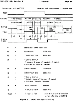
DA'l'BI Bu.s Cycles
-1. Timing for the .address portion of the cycle is given in 4.S.]. The Bus Master gates the negation of 'I'WTBT dong .. ith the assertion of TADDR onto the bus.
The Bus MIIsrer asserts the first TOIN UJIl ns minimLm after asserting TSYNC.
3. 'i'he Bus Master asserts re<;7 59 ns maximum aft .. r asserting TOIN for the first time. TBS7 ~ .... ains asserted until 59 ns maxilllUill after the assertion of TOIN for the last time. In each case, 1'857 can be asserted or negated as soon as the conditions for asserting TOIN are met.
DEC S'l'D 168. &!etian " 17-Sep-81 Paqe U.
I T ... ; . . . _ ... " .. OH".
~"o,_,_
...
ft . . R . . . "'"''''' ...i.5J . . . , ... _ ... _ . . . _
:.8
.
.. 1;I<1 ..,
...
'''''' ... 8\oo_ .... J . . . .'
...
"
...
~....
,;
..
DEC STIl 1611, Section tl 17-Sep-8l PIIIge 4S
4. The Bus Slave aSS·Hts TRIi'LY tl ns minim ... (8tltltl ns -maximum to avo~d Bus Tim<90ut) after the asserti:m of ROIN. The Bus Slave asserts TREE" COnCClt'rent with TRIi'LY if, and only If. i t 15 a ~~~~~n~~tN~eViCI! which can support another ROtH after the
5. The Bus Slave gates TOATA onto the bus tl ns minimum after the assertion of ROIN and 125 ms maxim ... after the assertion of TRPLY.
6. The Bus Master receives stable RDATA from 2tla ns maximum after the assertion of RRPLY until 211 ns minim ... ilIfter the neqation of ROlf.. ('I1le 2tl ns minim . . represents total minim ... receiver delays toor ROtH Cot the slave and RDo\TA at the Master.)
7. Thl! Bus Master negates TOni 2tl0 ns minimum after the assertion of RRP[,Y.
B. ~~N~uS Sli<vl! negates TRPLY a ns minim ... aftl!': t~e negation of
'J. I f RES7 and TREF arl! both asserted when TRPLY negates, the tlus Sli<ve .,repares for another RDIN cycle. RES7 is stable from 125 nsec aftet' RDIN asserts until 15" ns after TRPLY negates.
I f RES7 and TREF are not both assertr..:) when TRPLY neqates, the BuS Slave retOOves TDATA from t'le BUS " ns minim ... and Itltl ns maximlUl after negatil10J TRPLY.
If RREf' and TBS7 were both asset'tad when TOIN negated (above. timing relation.!:lhip 7). the Bus !'IiIster asset'ts TDIN 15tl ns minimum after RRPLY negates and continues with timing relationship 3 above. Ril.EF is stable frolll 75 nsec after RRPLY asserts until 20 [}s minim ... after '!'DIN negates. (The 2" ns minimum rept'esents total minim .... receiver delays for RUIN at the slave (lnd RR£F at the Mastet'.)
DEC STD 1611, Section e 17-5ep-81
S!Gr-.ALS AT BUS MASTER
I" I "I" I"
1;71;'
i"I "
I I
~=~~y----T Idfll,e) + ~=~~y----Tlp.op) +~=~~y----Tlreceive)+~=~~y----T (delay) +T Id"",,) +T Iprop) +T I.ect!,ve)
T(d'''/e) + (prop) +T Irece,ve) +T (delay) +T (drollt!+T (p.op) +T('ece,vel
14+16·t7+!9 -s,ncet1;mustbe>t5tormlS'ter tohavevahddata·andt9>tB
[image:48.204.25.179.16.232.2]DEC
sm
16e, Section e 17-Sep-81 Pac)e 474.5.2.2.5 DA'I'BO Bus Cycles
-1. Timing for the address portion of tho! cycle is given in 4.5.3. The Bus Master gates the assertion of the TWTBT aiong with the absertion of TADDR onto the bus.
2. The BllS Master gates TllATA and TW1'EIT onto the bus lllil ns minimum after TSYNC. 1Wl'BT is negated.
3. The Bus !".aster asserts TOOOT Uti! nS minim .... after gating TMTA onto the bus.
4. The Bus Slave receives stable RDATA and RWTaT from 25 ns minimLUII before the assertion of ROOl'T until 2S ns minimLUII after the negation of ROOUT.
5. The BUS Slave asserts TRPLY II ns mini'nWII after the as~rtion of RIlOUT. The Bus Slave asserts TREF concurrent with T"PL'f if, and only if. it is a block mode device which can support another ROOUT after the current RDOIJT.
6. The Bus Master negates TDOUT 1511 ns minimum after the assertion of RRPLY.
7. If RREF ... as asserted when RDOUT negat"d and the Bus Master wants to transmit more data in this Block Mode Cycle, then the Bus Master gat"s tt.e new TOATA onto the BUS 1110 ns minim ... after negating TOOUT. RRF;F is stable from 15 ns maxim .... after RRPL'f asserts until 211 nS minimum after RDIN negates. (The 211 ns minimun represents miniiD .... receiver delay.!! for RDIN at the slave and RRE:F at the /'Iaster.J
The Bus Master must limit itself to not more than eight transfers unless i t monitors RllMR. I f it monitors !UJotR, it may perform up to 16 transfers as long as RJ::MR is not asserted at the end of the seventh tr3nsfer.
B. If RREF was not asserted when 1'OOUT was negated or i f the Bus Master does not ... nt to transmit more data in this Block Mode ':ycle, then the Bus Master removes TllATA frOlll the bus
lee
ns minimum aftar negating TOOUT.9. ~u~~s Sl3ve negates TRPLY ~ ns minimlm after the nl!gation of