Abstract
Repeater insertion is a well established technique to minimise the propagation delay over long resistive inter-connect. In deep sub-micron technologies, as the wires are spaced ever closer and signal rise and fall times go into the sub-nano second region, increased cross talk has implica-tions on the data throughput and on signal integrity. Depending on the data correlation on the coupled lines, the delay can either decrease or increase. We show that in uni-form coupled lines, the response for several important switching patterns has a dominant pole characteristic. The effect of repeater insertion including optimal repeater insertion for minimising delay with worst-case cross-talk, and area constrained optimisation is considered. All equa-tions are checked against a dynamic circuit simulator (SPECTRE).
1. Introduction
Signal Propagation on long resistive interconnect lines is a function of the product of the line resistance and capaci-tance, commonly known as the RC delay. Since both the resistance and capacitance show a linear increase with length, the delay increases quadratically with length. Because the prophecy of Moore’s law in VLSI circuits has held true over the years, interconnections have become smaller in cross-section and longer in length with each suc-ceeding generation of CMOS technology resulting in a rap-idly increasing overall delay, especially in global wires. Hence there has been a lot of investigation into the problem of delay modelling [1] and repeater insertion in long inter-connect. Bakoglu [2] presented an analysis based on char-acterizing the repeater with an input capacitance and an output resistance which was one of the pioneering works in this area. Subsequently researchers have improved on both the repeater model and the wire load model. Wu and Shiau in [3] use a linearised form of the Schichmann-Hodges equations while Adler and Friedman in [4] use Sakurai’s alpha power model to include the effect of velocity
satura-tion in short channel devices. Ismail and Friedman in [5] present an analysis which models inductance in the inter-connect for the first time. In [6] Dhar and Franklin area present a mathematical treatment of area constrained opti-misation.
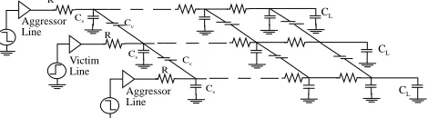
In the future generation of VLSI circuits when the fea-ture size shrinks to a fraction of a micro meter, the aspect ratio (width/height) of interconnect is reduced in order to keep the resistance increase to a minimum. This means however that the capacitance between wires increases and cross talk will pose a serious challenge in designing VLSI systems. Cross talk couples a noise voltage onto the victim net, and has as an effect on the delay. Our interest in this paper is in cross-talk induced delay, and further in a paral-lel line configuration, where the nets are laid out alongside each other for a relatively long distance as would occur in an intermediate or global level bus. Recently there has been a profusion of research into block level architectures with each block containing 50k to 100k gate modules [7]. These blocks communicate with each other via global level inter-connects, either through buses or dedicated links. Regard-less of the exact high-level signaling protocol, the parallel net topology in Fig. 1 will occur very often.
Capacitive coupling between lines can result in speeding up of the signal or cause delay- depending on the correla-tion between the data on the different lines. This input dependent dynamic delay can exactly be captured only by dynamic simulators, which are costly in terms of computa-tion resources such as CPU time and memory. When the line under consideration is reduced to a uniformly coupled two aggressor configuration as shown in Fig. 1, certain simplifications are possible which allow delay predictions depending on the switching of the aggressors. One of the most widely used techniques is to lump together the total capacitance and use a coefficient which changes to differ-entiate between switching and quiet aggressors. There have been previous works which have distributed the capaci-tance over ground and coupled components and presented closed form delay equations with ramp inputs. However these use a single T orΠsection, which does not represent
On Dynamic Delay and Repeater Insertion in Distributed Capacitively
Coupled Interconnects
11. The funding support of Sida and that of Vinnova via the Socware and Exsite Programs are gratefully acknowledged
Dinesh Pamunuwa and Hannu Tenhunen
Royal Institute of Technology (KTH), IMIT, LECS Electrum 229, SE-164 40 Kista, Sweden
a distributed line with reasonable accuracy.
We present in this paper an analysis of delay in parallel capacitively coupled interconnects with simultaneously switching aggressors. We distribute the capacitance over ground and coupled components, and consider true distrib-uted lines. Simple first order expressions for a variety of switching patterns giving accurate measures of average, best and worst-case delay for buffered lines are derived. These delay models show how repeater insertion can be optimised to compensate for dynamic effects, and are suita-ble for initial timing estimates. Area constrained optimal repeater insertion is also considered.
2. Delay Model for Coupled Interconnects
From now on, whenever delay is mentioned we are always talking about the 50% delay, since this is the delay to the switching threshold of an inverter. Also in all cases the victim line is assumed to switch from zero to one, with-out loss of generality. When a line switches up(down) from zero(one) it is assumed to have been zero(one) for a long time. We consider a line with coupling on two sides as shown in Fig. 1. The reason is that this is closest to the actual situation for an interconnect in a bus.
To build up our delay model for the distributed line, we analyse first the lumped model which consists of the first section of Fig. 1. For simultaneously switching lines, six different switching scenarios can be identified.
(a) Both aggressors switch from one to zero (b) One switches from one to zero, the other is quiet (c) Both are quiet
(d) One switches from one to zero, the other switches from zero to one
(e) One switches from zero to one, the other is quiet (f) Both switch from zero to one
Consider (c) above as the reference delay, where the driver of the victim line charges the entire capacitance. Cases (a) and (b) slow down the victim line, (d) is equiva-lent to (c), and (e) and (f) speed up the victim. Now given in (1) is the complete response of the victim line. Depend-ing on how the aggressor lines switch, the coefficients Ai and Bi take the values given in Table 1.
In cases (b) and (f), the response is a single decaying exponential with a time constant of R(Cs+3Cc), while in the other cases this is the slower time constant. In cases (a), (c) and (d), this slower time constant is also associated with the larger coefficient, and hence becomes a truly dominant time constant. This is especially so in case (a). Typically in current and future sub-micron technologies with high aspect ratio interconnect, Ccis close to Csand often greater. The accuracy of the single time constant is compromised only when Cc << Cs when there is no need to distribute the capacitance anyway.
Now to state some well known results, a lumped RC cir-cuit has a single pole response and the delay is as given in (2). Signal propagation along a distributed RC line is gov-erned by the diffusion equation which does not lend itself readily to closed form predictions for the delay at a given threshold. However it turns out that a simple exponential is a very good predictor [1]. The reason is that a distributed line (which comprises cascaded RC sections in the limit where the number of sections tends to infinity) is a degen-erate version of an RC tree. The transfer function in conse-quence has a dominant pole which can be well approximated by the reciprocal of the first moment of the impulse response. The first moment of the impulse response is 0.5RC which leads to (3) as the model for the 50% delay of a distributed RC line to a step input. This is a very good approximation and is reputed to be accurate to within 4% for a very wide range of R and C.
In general whenever the response of the lumped model corresponding to a single section of the distributed line is or can be approximated by a waveform containing a single exponential, most of the response of the distributed line can also be approximated by a waveform with a single
expo-Figure 1. Configuration for investigating effect of
cross talk
Cc Cs
Cs
Cs Cc R
R
R
CL
CL
CL
Aggressor Line
[image:2.595.54.289.75.140.2]Aggressor Line Victim Line
Table 1. Coefficients for different switching patterns
i Switchingpattern Ai Bi λi µi
1 (a) -4/3 1/3 1.51 2.20
2 (b) 1 0 1.13 1.50
3 (c) -2/3 -1/3 0.57 0.65
4 (d) -2/3 -1/3 0.57 0.65
5 (e) -1/3 -2/3 --
--6 (f) 0 1 0 0
V 1 Aie t R C( s+3Cc) ---–
Bie t RCs
---–
+ +
= (1)
T0.5 lumped, = 0.7RC (2) T0.5 distr, = 0.4RC (3)
nential. Hence we propose to approximate the delay of the
distributed lines corresponding to (a), (b), (c), (d) and (f)
with single time constant expressions. (In the case of (e) because the lumped model does not have a dominant time constant, the accuracy is not high enough to justify such an approach). Since the time constants in question are linear combinations of R, Csand Cc, changing coefficients are suf-ficient to distinguish between the different cases. The delay is as given in (4) whereλi take the values in Table 1.
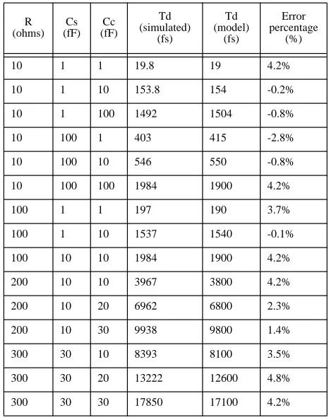
These constants were obtained by running sweeps with the circuit analyser SPECTRE. It can be seen that putting the coupling capacitance to zero in (4) results in (3). For all
i, the accuracy is more than 95% for a wide range of R, Cs and Ccvalues. In the interest of brevity, only values for i=1, which is of special interest, is shown here in Table 2. These values are a representative subset of the values used, giving both relatively large and small variations in the parameters to show that there is good agreement for a wide range. In the simulations, a distributed line was modelled by cascad-ing a number of T sections. It is well known that the accu-racy of a T-n orΠ-n model for a distributed RC line grows rapidly with n. We used a sufficiently large number of sec-tions such that the improvement gained in adding a section was less than 0.1%. For all practical purposes, (4) is as accurate as the very commonly used approximation given in (3) and shows very succinctly the effect of switching aggressors on the delay of the victim line. Although only step inputs have been considered, we will go on to show that typical line delays are much greater than signal rise(fall) times, and hence the rise(fall) time manifests itself as a constant. This delay model is used in the next section to investigate the effect that repeater insertion has on the total delay in such capacitively coupled lines when the aggressors switch in the different ways.
3. Repeater Insertion
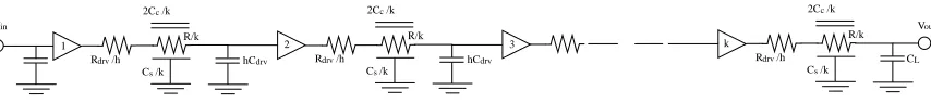
To reduce delay the long lines in Fig. 1 are broken up into shorter sections, with a repeater (an inverter) driving each section as shown in Fig. 2. The analysis for repeater insertion is carried out by characterizing the non-linear buffers by an output resistance Rdrv, and input capacitance Cdrv. Hence the buffers are approximated by voltage sources with series resistances, and an input capacitance which loads the previous buffer. This allows the use of superposi-tion to find the total delay. For a single secsuperposi-tion, the delay is given by (5). This expression follows the Bakoglu model [2] of equalising the repeaters, and can be explained as fol-lows. The distributed and lumped resistances combine with
the distributed and lumped capacitances to produce various delay terms. The terms in bold are the result of modelling cross talk in the delay.λiandµitake the values given in Table 1, where µiis a coefficient introduced to take the Miller effect into account.1
The lumped resistance Rdrv combines with all the capacitances (lumped and distrib-uted) to produce delay terms with a coefficient of 0.7. Sim-ilarly the distributed resistance of the line combines with various capacitances to produce different delay terms. (it is assumed that the load at the end of the line is an inverter which is the same size as the driving inverter). The accu-racy of this delay expression was checked against simu-lated values, and the results are presented in Table 3. Here
Rdrvand Cdrvare chosen as 1kΩand 10f F as being repre-sentative values for a buffer. Again only a subset of the val-ues pertaining to case (a) are shown, but it can clearly be seen that (5) is as accurate as the initial expression (4).
Now let the number of repeaters including the original driver be k, and the size of each repeater be h times a mini-mum sized inverter (all lines are buffered in a similar fash-ion). The output impedance of a minimum sized inverter
[image:3.595.313.546.98.395.2]T0.5 distr, = 0.4RCs+λiRCc (4)
Table 2. Comparison of actual delay and delay predicted by model for a distributed RC line with cross talk
R (ohms)
Cs (fF)
Cc (fF)
Td (simulated)
(fs)
Td (model)
(fs)
Error percentage
(%)
10 1 1 19.8 19 4.2%
10 1 10 153.8 154 -0.2%
10 1 100 1492 1504 -0.8%
10 100 1 403 415 -2.8%
10 100 10 546 550 -0.8%
10 100 100 1984 1900 4.2%
100 1 1 197 190 3.7%
100 1 10 1537 1540 -0.1%
100 10 10 1984 1900 4.2%
200 10 10 3967 3800 4.2%
200 10 20 6962 6800 2.3%
200 10 30 9938 9800 1.4%
300 30 10 8393 8100 3.5%
300 30 20 13222 12600 4.8%
300 30 30 17850 17100 4.2%
1. Because of the approximate delay models used for a
for the particular technology is Rdrv,mand the output capaci-tance Cdrv,m. Then the output impedance of an h sized driver is assumed to be Rdrv,m/h, and the output capacitance h*Cdrv,m. This configuration is sketched out in Fig. 2, where the symbol refers to a capacitively coupled intercon-nect as shown in Fig. 1. Now with reference to Fig. 3 and again using superposition with the delay equations (2, 3 and 4) the total delay takes the expression given in (6). It is assumed that the load CLis equal to the input capacitance of an h sized inverter. Also the signal rise time has been included here. Because in general the delay per section is much greater than half the rise time, the non-zero rise(fall) time of the input signal is reflected in (6) as a simple addi-tion. Hence the fact that the entire analysis is based on step inputs does not affect the accuracy of the final expressions seriously. This is ever more true for future generations of technologies where decreasing feature sizes allow transis-tors to be gated with faster signals, but also cause wire par-asitics to become more pathological.
4. Minimum Delay
Now to find the optimum h and k for minimising delay, the partial derivatives of (6) with respect to k and h are equated to zero, resulting in (7) and (8). Note that when the coupling capacitance term Ccis set to zero (i.e. the entire capacitance is lumped into the term Cs), (7) and (8) sim-plify to the Bakoglu equations [2]. Case (a) is of special significance because it represents the worst-case cross-talk of all the cases considered. It does not cause the worst case delay, because even for the simple case of uniformly cou-pled lines, both aggressors switching slightly after the vic-tim causes the worst delay. This worst-case delay is however only about 3% greater on average than that caused by simultaneously switching aggressors, and hence (a) can be considered to give the worst-case delay for all practical purposes. If the timing constraints are such that the worst-case delay needs to be minimised, h1,optand k1,optshould be the repeater insertion strategy. If the constraints are less stringent, h and k can be relaxed. Whatever the values that
h and k are eventually chosen to be, (6) can be used to
pre-dict the delay.
5. Area and Power Considerations
The area of a minimum sized inverter can be modelled as the sum of two components, one of which is dependent on the W/L ratio of the transistors, and one which is independ-ent of it. Now since the repeaters are h times a minimum sized inverter and are k in number, minimising the area is equivalent to minimising the product hk. The dynamic power consumption of an inverter is 0.5CloadVdd
2
f (where f
refers to frequency), and hence for a given frequency power consumption is minimised by minimising Cload. Since the output capacitance of an inverter is proportional to h, minimising power consumption is also equivalent to minimising hk.
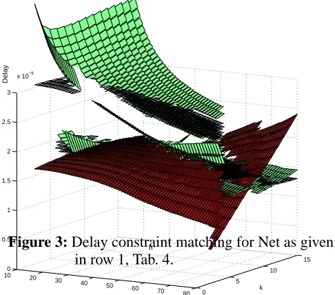
The problem of repeater optimisation can take two forms. Either the maximum acceptable delay for the net is specified, and the objective is to minimise area subject to the constraint t≤ tmax, or the maximum acceptable area is specified and the objective is to minimise the delay subject to the constraint A≤Amax. Consider Fig. 3 which shows the variation of delay with h and k where the line parasitics correspond to row 8 of Table 4. The plane shows the delay Table 3. Accuracy of delay model for section
R (ohm) Cs (fF) Cc (fF) Error Percentage
10 10 1 -2.1%
10 10 10 2.2%
100 100 100 2.6%
200 10 10 2.7%
200 55 10 -1.0%
200 100 10 -1.7%
400 10 100 -1.9
600 55 55 3.3%
1000 100 1 -0.6%
Cs/k 2Cc/k
R drv/h hCdrv
R/k
Cs/k 2Cc/k
R drv/h hCdrv
R/k
Cs/k 2Cc/k
R drv/h
R/k
1 2 3 k
CL
[image:4.595.88.515.70.118.2]Vin Vout
Figure 2: Repeater insertion in a long interconnect
t0.5 k 0.7
Rdr vm
h
--- Cs
k
--- hCdr vm µi
2Cc
k
---+ +
R
k
--- 0.4Cs
k
--- λiCc
k
--- 0.7hCdr vm
+ +
+ =
(6) tr
2 ---+
t0.5 sec, = 0.7Rdrv(Cs+Cdrv+µi×2Cc)+R 0.4C( s+λi×Cc+0.7Cdrv)
(5)
ki opt, 0.4RCs+λiRCc
0.7Rdr vmCdr vm
---= (7) h
i opt,
0.7 Rdr vmCs+1.4µiRdr vmCc
0.7RCdr vm
---= (8)
constraint of 1.3n seconds for that net, and any of the k and h combinations which lie below this and on the curved sur-face showing the delay is acceptable to meet the delay con-straint. Also shown is an appropriately scaled plot of hk.
Because hk is quasi concave in the quadrant of positive h and k, it is not possible to find an analytical solution to the first optimisation problem, which has to be solved numeri-cally. However it is possible to analytically solve the sec-ond optimisation problem because its objective function t0.5 as given in (6), is concave as seen in the figure. The opti-mum solution can be found by solving the Kuhn Tucker conditions given by the following equations.
6. Testing with Real Repeaters
We investigated the accuracy of our models with an actual 0.35µm AMS technology. The input capacitance of a minimum sized inverter in that technology is approxi-mately 9.5f F while its output impedance is 7.7k ohm. We used signal rise and fall times of 100p seconds. In the same technology, a 1 cm long wire in metal 3 has a total capaci-tance to substrate of 720f F, a coupling capacicapaci-tance of 850f F to an adjacent wire with minimum spacing, and a resist-ance of 800 ohm. Hence the loads in Table 4 are chosen to represent global or semi global length wires. The repeater
insertion strategy we have opted to show here is h1,optand k1,opt, and the accuracy is tested for case (a).
The main source of the error is the result of treating the inverter as a voltage source-resistor-capacitor combination where the parasitics scale linearly with size, and ignoring all second order effects. Though poor, it is a widely used approximation, and the first order line delay approxima-tions presented here are really quite accurate in compari-son. Shown in Fig. 4 are the results of simulations for a range of h situated either side of the value predicted by (6).
10 20
30 40
50 60
70 80 0
5 10
15 0
0.5 1 1.5 2 2.5 3
x 10−9
k h
Delay
Figure 3: Delay constraint matching for Net as given in row 1, Tab. 4.
0.7Rdrv
h2
--- C( s+4.4Cc)–0.7RCdrv+L1k+L2 = 0
R
k2
--- 0.4C( s+1.5Cc)–0.7RdrvCdrv+L1h+L3 = 0
L1(hk–Amax) = 0 hk≤Amax L1≥0
L2(h–1) = 0 h≥1 L2≥0
L3(k–1) = 0 k≥1 L3≥0
(9)
(10)
(11)
(12)
[image:5.595.344.591.9.200.2](13)
Table 4. Comparison of model for buffered net with worst-case cross-talk against actual delay with real inverters
R (ohms)
Cs (fF)
Cc
(fF) k h
Td (actual)
(ps)
Td (model)
(ps)
Error %
600 550 100 2 37 694.6 555 13.9%
800 100 100 2 23 616.9 477 15.8%
1k 100 100 2 21 665.3 526 14.6%
600 550 550 3 63 1053 918 8.5%
800 1000 100 3 38 957.4 757 16.6%
1k 550 100 3 28 894.2 704 16.6%
600 550 1000 4 82 1408 1165 14.2%
800 550 550 4 55 1303 1047 16.4%
1k 10 10 4 45 1310 1072 14.9%
600 10 10 5 86 1520 1216 17.3%
1k 10 20 5 49 1475 1168 18.0%
1k 10 30 5 53 1555 1251 16.9%
26 28 30 32 34 36 38 40 42 44
6.5 7 7.5 8 8.5 9 9.5
10x 10
−10 Variation of Delay with h
h
Time / seconds
R=800 Ohm, Cs=1p F Cc=100f F, k=3, h=38
[image:5.595.58.301.28.242.2]R=600 Ohm, Cs=550f F Cc=100f F, k=2, h=37
It shows that the delay curves are quite flat, and k and h can be relaxed with little loss in performance.
7. Statistical Analysis of Delay
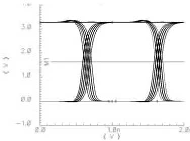
To investigate the effect of aggressor alignment (the time at which they switch relative to the victim net) and the “memory” effect of the RC channels on delay, we use eye diagrams built up over hundreds of cycles. By processing these eye diagrams, it is possible to estimate the delay and to see clearly the speed-up and slow-down effect of the switching aggressors. In the configuration shown in Fig. 3, instead of ramp inputs the nets are driven by different pseudo-random bit sequences (PRBS) as would occur in an actual situation. Shown in Fig. 6 is the eye diagram corre-sponding to row 1 in Table 4. The period of the wave form is 1n second.
The 50% point is given by the intersection of the marker with the waveforms. The smearing of the walls is caused by the aggressors switching in random fashion and having var-ying effects on the delay. The maximum delay is defined by the right boundary of the first wall, and is 712p seconds. Table 4 shows that when all nets switch simultaneously the delay is 695p seconds. So this is an increase of 2.5% on the value given by simultaneously switching nets, where the increase is mainly due to the memory effect, as a pulse width of 1n second for a line which has a delay of about 0.7n second does not allow the line to discharge ade-quately.
8. Summary
In this paper we have investigated the issue of dynamic delay in buffered lines. We presented a dominant time con-stant response for the important configuration of parallel coupled interconnects where a changing coefficient can be
used to model the effect of simultaneously switching aggressors. We have used this model to study the impact of cross talk on buffer sizing for delay minimisation in long nets, and derived a new set of equations that show how the delay changes with the size and number for different switching patterns. All equations were checked against a dynamic circuit simulator SPECTRE, and the accuracy of the repeater models were checked using real transistor models from an actual 0.35µm process.
The expressions we derived for the intrinsic line delay are simple, yet useful and represent an improvement over models used to estimate the effect of cross-talk on delay in current static timing analysis tools, which do not distribute the capacitance, and use a coefficient which takes one of two values to differentiate between quiet and switching nets. The use of these models to analyse the delay in buff-ered nets is a novel approach, resulting in some further expressions which greatly facilitate repeater optimisation under different constraints.
9. References
[1] Rubinstein J. et al., “Signal Delay in RC tree net-works”, IEEE Transactions on Computer Aided Design, vol CAD-2, no. 3, pp. 202-211, july 1983.
[2] Bakoglu H. B., “Circuits, Interconnections, and Pack-aging for VLSI”, Addison Wesley 1990
[3] Wu C. Y. and Shiau M., “Accurate speed improvement techniques for RC line and tree interconnections in CMOS VLSI”, in proc. IEEE International Symposium on Circuits and Systems (ISCAS) 1990, pp. 2.1648-2.1651.
[4] Adler V. and Friedman E. B., “Repeater Design to Reduce Delay and Power in Resistive Interconnect”, in IEEE Transactions on Circuits and Systems-II, Analog and Digital Signal Processing, Vol. 45, No. 5, May 1998
[5] Ismail Y. I., and Friedman E. G., Effects of Inductance on the Propagation Delay and Repeater Insertion in VLSI Circuits, IEEE Transactions on VLSI Systems, April 2000, vol. 8, pp. 195-206
[6] Dar S, Franklin M. A., “Optimum Buffer Circuits for Driving Long Uniform Lines”, IEEE J. Solid State Cir-cuits, vol. 26, pp. 32-40, Jan. 1991.
[7] 13) Dennis Sylvester and Kurt Keutzer, “Getting to the Bottom of Deep Submicron II: A Global Wiring Para-digm” Proceedings of International Symposium on Physical Design, 1999, pp. 193-200.
[image:6.595.67.255.80.219.2][8] Dinesh Pamunuwa and Hannu Tenhunen, “Repeater Insertion to Minimize Delay in Parallel Coupled Inter-connects”, In proc. of the 14th International Conference on VLSI Design, Jan. 2001.
Figure 5: Eye Diagram for Net as given in row 1, Tab. 4