Design, Optimization and Synthesis of Efficient
Reversible Logic Binary Decoder
Ravish Aradhya HV
Dept of ECE RVCE Bangalore, India
Chinmaye R
Dept of ECE RVCE Bangalore, India
Muralidhara KN
Dept of ECE PESCE Mandya, India
ABSTRACT
Reversible logic is an emerging research area. Interest in this field is motivated by its applications in several technologies involving low voltages and low power. Binary reversible circuits have been studied for their potential application in low-power CMOS design, quantum computation, nanotechnology, optical computation, etc. In this paper, a Reversible low power Decoder is proposed, newly proposed decoder compared with already proposed reversible decoder and the Conventional decoder. Circuits have been designed and synthesized using Rev Kit. The circuits are simulated in cadence too and Power consumption is calculated using cadence for all three designs. The performance analysis is verified using number of reversible gates, Garbage outputs, Transistor cost, Line cost power consumed and Quantum Cost. Improvement in the area of the proposed decoder as compared to the conventional one can be shown to be 33.33% and total power of 9.44%. Also an algorithm for NX2N decoder is given.
General Terms
Constant input, Power optimization
Keywords
Feynman Gate, Fredkin Gate, Garbage output, Line cost, Quantum Cost, Reversible Logic.
1.
INTRODUCTION
An observation was made by Intel co-founder Gordon Moore in 1965. He noticed that the number of transistors per square inch on integrated circuits had doubled every year since their invention. Moore‟s law predicts that this trend will continue into the foreseeable future. The number of transistors per square inch doubles approximately every 18 months. The motivation for low power design includes higher functionality with small sized chips, Higher performance at lower cost, hand held devices powered by batteries, New portable compute-intensive applications such as Multi-media, Video capture and display, Handwriting recognition, Notebook computer, Personal data assistant, Laptops, Hand held mobile phones, Implantable medical electronics etc. Low power has emerged as a principal theme in today's electronics industry. The need for low power has caused a major paradigm shift in which power dissipation is as important as performance and area. Power optimization can be done at various abstraction levels in CMOS VLSI i.e. at Device (Technology) level, Circuit level, Logic level, Architecture (System) level, Algorithmic level, etc. One such method at circuit logic level is energy recovery method, which employs reversible logic gates.
Reversible computing was found on the basis of thermodynamics of information processing; it was shown that conventional irreversible circuits unavoidably generate heat
because of loss of information during the computation. Reversible computing is based on two concepts: logical reversibility and physical reversibility. Irreversible erasure of a bit in a system leads to heat generation. A computational operation is said to be logically reversible if the input of the system can be retrieved from the output obtained from it. An operation is said to be physically reversible if it converts no energy to heat and produces no entropy.
According to R. Landauer‟s research [2], energy (heat) of kT ln 2 is dissipated for every Irreversible bit operation, where k is the Boltzmann‟s constant (1.3807×10⁻²³
JK-1) and T is the operating temperature. For T equal to room temperature (300 K), kT ln2 is approximately 2.8×10⁻²¹ J, which is small but non-negligible. In 1973, C. H. Bennett[1,3] concluded that no energy would dissipate from a system as long as the system was able to return to its initial state from its final state regardless of what occurred in between. It made clear that, for power not to be dissipated in the arbitrary circuit, it must be built from reversible gate. Reversible circuits are of particular interest in low power CMOS VLSI design.
[image:1.595.320.513.534.689.2]A Decoder is a fundamental building block in many computing systems which can take the form of a multiple-input, multiple-output logic circuit that converts coded inputs into coded outputs, where the input and output codes are different, for example n-to-2n. A 2x4 decoder is shown in Figure 1. A nx2n type binary decoder converts binary information from 'n' coded inputs to a maximum of 2n unique outputs.
2.
REVERSIBLE GATES
[image:2.595.54.275.73.186.2]A. Feynman / CNOT Gate
Figure 2: Feynman/CNOT Gate (FyG)
The Reversible 2*2 having mapping input (A, B) to output (P,Q) is as shown in the Figure 2.
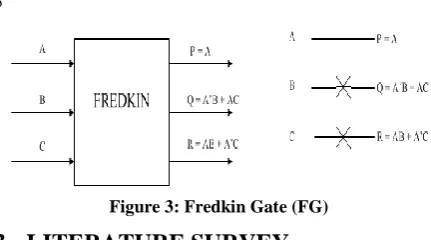
B. Fredkin Gate
[image:2.595.57.273.265.385.2]Reversible 3*3 gate maps inputs (A, B, C) to outputs (P=A, Q=A'B+AC, R=AB+A'C). Fredkin gate is as shown in Figure 3
Figure 3: Fredkin Gate (FG)
3.
LITERATURE SURVEY
Enoch Hwang et all [4] showed that although power reduction techniques can be applied at every level of design abstraction, most automated power reduction techniques apply to the lower levels of design abstraction, such as the register-transfer or gate level. They have demonstrated through several experiments that functional partitioning, has already been shown to yield improvements in solving problems of I/O constraint satisfaction, synthesis complexity, and hardware/software partitioning, can also yield substantial reduction in power consumption (on average 41% total power reduction) with some overhead in size and performance. Yeong-Kang Lai, et al have showed [5] a new method for reversible variable length coding (RVLC) decoding. Alberto Nannarelli and Tomás Lang [6] have illustrated some techniques such as such as switching-off non active blocks, retiming, dual voltage, and equalizing the paths to reduce glitches for dividers realized in CMOS technology and energy dissipation reduction is carried out at different levels of abstraction: from the algorithm level down to the implementation or gate level. Lafifa Jamal, et all [7] proposed the compact design of reversible circuits for a data acquisition and storage system. The design comprises with a compact reversible analog-to-digital converter and a reversible address register. In the way of designing this data acquisition and storage system they have proposed a reversible J-K flip-flop with asynchronous inputs, a reversible D flip-flop and a reversible three state buffer register. All the reversible designs individually have less number of gates, garbage outputs and quantum cost compared with the existing ones. S B Rashmi et all [8] proposed an improved design of a 4 x 4 multiplier using reversible logic gates. It is faster and has lower hardware complexity compared to the existing designs. In addition, the proposed reversible multiplier is good in terms of number of gates, number of garbage outputs, number of constant inputs and quantum cost. Morrison et al [9] have proposed novel 4x4 RD gate implemented as a 2-to-4 decoder
with low delay and cost, and a novel 4*4 R2D gate used in the implementation of a novel n-to-2n decoder with low cost and delay. A reversible synchronous up-down counter is presented and verified, and a reduced reversible implementation of a JK Flip Flop is implemented in a reduced reversible synchronous up-down counter. This decoder and counter are then utilized in the design of a reversible Moore finite state machine. Mozammel H. A. Khan [10] has shown the reversible realization of decoder multiplexer and de-multiplexer using quaternary reversible gates like quaternary shift gates (QSG), quaternary controlled shift gates (QCSG), and quaternary Toffoli gates (QTG). In [11], it is shown that it is possible to build sequential circuits with zero internal power dissipation. In [12] 2x4 decoder is realized using 3 Fredkin gates. The software used for simulation: REVKIT and CADENCE.
4.
DESIGN
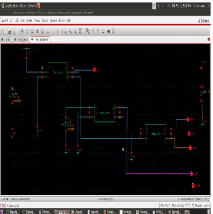
A Conventional Decoder symbol is as shown in the Figure 4. The design of a 2x4 Conventional decoder requires 2 BUFFERS (2 inverters connected in series forms a BUFFER), 2 INVERTERS and 4 AND (Nand gate followed by an inverter is an AND gate) gates. This design requires a total of 8 gates. The total number of inputs is 2 and the total number of outputs 4. Construction of Conventional 2x4 decoder in cadence and the simulation results are as shown in Figure 5 and Figure 6 respectively.
Calculation of power dissipation was performed in cadence for the conventional 2x4 decoder. Circuit is constructed using 90nm technology. Static power dissipated in the design is 2.298 micro watts. Total power dissipated when the circuit is simulated for 80ns is 7.891 micro watts. Hence the total dynamic power dissipated through a conventional 2x4 decoder is 5.593 micro watts neglecting the power dissipation due to leakage currents.
Figure 4: A 2x4 Decoder
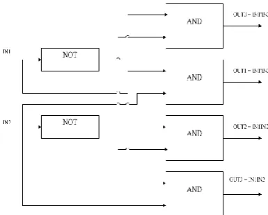
The decoder proposed in [12] is constructed using only Fredkin gates and is as shown in Figure 7.
[image:2.595.320.537.423.696.2]which 2 are garbage outputs. Here OUT3 that represents IN1IN2, OUT1 that represents IN1‟IN2, OUT2 that represents IN2‟IN1 and OUT0F that represents IN1‟IN2‟ are the required outputs. IN1 and IN2 are the garbage outputs. The circuit of 2x4 Decoder constructed using Fredkin gates is shown in Figure 8. The inputs CONST1, CONST2, CONST3 and CONST4 are the constant inputs where the values of CONST2, CONST3 and CONST4 are set to Zero and CONST1 is set to one.
Figure 5: Conventional 2x4 Decoder
Simulation results from RevKit are as shown in the Figure 9. The circuit diagram of the 2x4 decoder in cadence is as shown in Figure 10.
Calculation of power dissipation was performed in cadence for the 2x4 decoder using 3 Fredkin gates. Circuit is constructed using 90nm technology.
Static power dissipated in the design is 1.49 micro watts. Total power dissipated when the circuit is simulated for 80ns is 7.264 micro watts. Hence the total dynamic power dissipated through the reversible 2x4 decoder is 5.774 micro watts neglecting the power dissipation due to leakage currents.
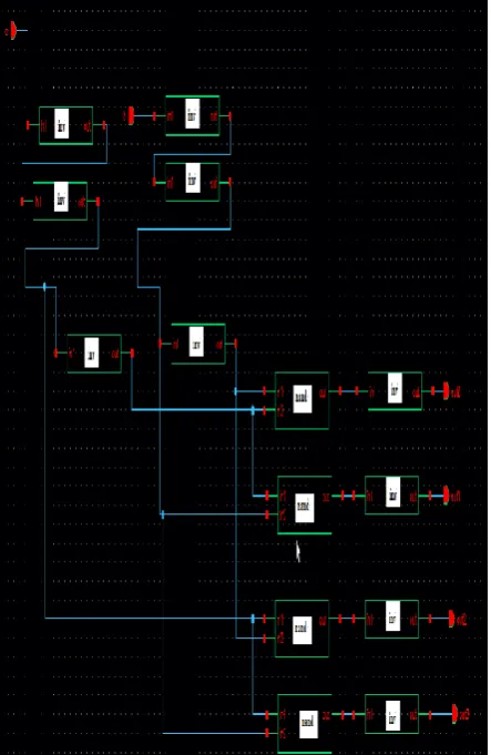
[image:3.595.57.279.169.510.2]The proposed design of a 2x4 Decoder requires 1 Feynman and 2 Fredkin Gates. This is as shown in Figure 11. This design requires a total of 3 gates. The total number of inputs is 5 which include 2 variable inputs and 3 constant inputs. Total number of outputs is 5, out of which 1 is garbage output. Constant inputs include 1 one and 2 zeros. The circuit of 2x4 Decoder constructed using Feynman gates and Fredkin gates is shown in Figure 12.
Figure 6: Simulation results of a conventional 2x4 decoder
Figure 7: Reversible Decoder using Fredkin gates
Figure 8: Circuit of Reversible Decoder using FGs
[image:3.595.317.539.370.484.2] [image:3.595.366.487.535.688.2]Figure 9: Simulation results Reversible Decoder using Fredkin gates in rev kit
Simulation results from RevKit are as shown in the Figure 13. Calculation of power dissipation was performed in cadence for the 2x4 decoder using Feynman and Fredkin gates. Circuit is constructed using 90nm technology. Static power dissipated in the design is 1.512 micro watts. Total power dissipated when the circuit is simulated for 80ns is 7.146 micro watts. Hence the total dynamic power dissipated through the reversible 2x4 decoder is 5.634 micro watts neglecting the power dissipation due to leakage currents.
[image:4.595.327.528.68.242.2]Figure 10: Circuit diagram of Reversible Decoder using Fredkin gates in cadence
[image:4.595.319.536.274.529.2]Figure 11: Reversible Decoder using Feynman and Fredkin gates
[image:4.595.59.277.365.584.2]Figure 12: Circuit of Reversible Decoder using Feynman and Fredkin gates
Figure 13: Simulation results Reversible Decoder using Feynman and Fredkin gates in Revkit
5.
GENERAL DESIGN AND
ALGORITHM OF A REVERSIBLE
DECODER
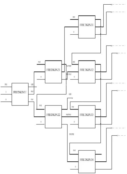
A Nx2N decoder can be designed using only Fredkin gates as shown in the Figure 14. This requires 2N – 1 Fredkin gates i.e. 1:2 decoder uses 1 Fredkin gate with the inputs as IN1, 1, 0. The outputs are IN1, IN1‟, IN1. Here the 2nd output (IN1‟) and the 3rd output (IN1) are the required outputs and the first
output (IN1) is the garbage output. The total number of constant inputs required are 2N ,out of which 2N – 1 zeros are
required and the number of one‟s required is one. In case of 1:2 decoder there are 2 constant inputs which includes 1 one and 1 zero. There are „N‟ garbage outputs. In case of 1:2 decoder there is one garbage output.
Algorithm for Nx2N decoder is as follows
[image:4.595.56.276.618.712.2]Fredkin22 ( In2, out3 of Fredkin11, 0) ;
Fredkin31 ( In3, out2 of Fredkin21, 0) ; Fredkin32 ( In3, out3 of Fredkin21, 0) ;
Fredkin33 ( In3, out2 of Fredkin22, 0) ; Fredkin34 ( In3, out3 of Fredkin22, 0) ;
[image:5.595.341.539.79.302.2]
FredkinN(N-1) (InN, out2 of Fredkin(N-1)(N-1), 0) ; FredkinNN (InN, out3 of Fredkin(N-1)(N-1), 0) ;
Figure 14: General Design of the Decoder
The design of a 3x8 Reversible decoder that is derived from the general design of the decoder is as shown in the Figure 15. The design requires 7 Fredkin gates, 56 transistors, 8 constant inputs with 7 constant inputs as zero and 1 constant input as one, 3 Garbage outputs, 11 lines. The quantum cost of 3x8 decoder is 35. The circuit diagram of a reversible 3x8 decoder as drawn in Rev Kit is as shown in the Figure 16. One of the simulation result when all inputs are zero (IN1=0, IN2=0, IN3=0) is as shown in Figure 17.
6.
RESULTS AND DISCUSSION
Comparison of different architectures of Decoders is shown Table-1.
[image:5.595.59.282.249.553.2]The comparative study between the decoder in [12] and the proposed decoder shows an improvement in quantum cost,
Figure 15: Design of a 3x8 Reversible Decoder
Figure 16: Circuit of a 3x8 Reversible Decoder
[image:5.595.338.557.323.525.2] [image:5.595.332.560.546.731.2]line cost and garbage outputs. The quantum cost (QC) of the proposed decoder is 12 where as that in [12] is 15. Line cost (LC) is 5 in the proposed decoder where as it is 6 in [12]. Garbage output (GO) is one in the proposed decoder against 2 in [12]. The Constant Inputs (CI) of the proposed decoder is 3 where as that in [12] is 4 with the „ENABLE‟ pin being set to one. However the Gate cost (GC) and the Transistor cost (TC) of both the designs are the same.
Table-1: Comparison of proposed decoder and design in [12]
GC QC TC LC GC CI
In [12] 3 15 24 6 1 4 Proposed
Decoder 3 11 24 5 2 3
Figure 18: Comparison of various parameters of the proposed decoder and in [12]
It is evident that the proposed design has an improvement of 20% in terms of quantum cost, 16.66% in terms of line cost and 50% in terms of garbage outputs. Figure 18 shows the graph representing the same.
Table-2 Comparison of Proposed decoder with conventional Decoder and in [12]
Transistor count Static Power Dynamic Power Total Power
In [12] 24 1.49E-06
5.774E-06
7.26E-06 Conventional
Decoder 36
2.298E-06 5.593E-06 7.89E-06 Proposed
Decoder 24
1.512E-06 5.634E-06 7.15E-06 % improvement WRT Conventional
Decoder 33.33 33.85 -0.7 9.44
%
Improvement
WRT [12] 0 -1.47 2.245 1.6
The proposed decoder uses only 24 transistors as compared to 36 in conventional one. The % improvement in area, static power and total power as compared to conventional decoder is 33.33, 33.84 and 9.44 respectively. The % improvement of dynamic power and total power as compared to [12] are 2.245 and 1.46 respectively. Figure 19 and 20 shows the graph
[image:6.595.316.543.135.272.2]In future an attempt can be made to decrease the power dissipation. Communication channels that require encoding of the messages at the transmitter end and decoding of the messages at the receiver end can be built using reversible decoders.
Figure 19: Comparison of Transistor cost of proposed decoder with conventional decoder and design in [12]
Figure 20: Comparison of power consumption of Proposed decoder with conventional decoder and design in [12]
7.
REFERENCES
[1] C.H. Bennett, “Logical Reversibility of Computation”, IBM Journal of Research and Development, pp. 525-532, November 1973
[2] R. Landauer, “Irreversibility and Heat Generation in the Computational Process”, IBM Journal of Research and Development, 5, pp. 183-191, 1961.
[3] C.H. Bennett, "Notes on the History of Reversible Computation", IBM Journal of Research and Development, vol. 32, pp. 16-23, 1998.
[4] Enoch Hwang, Frank Vahid, Yu-Chin Hsu, “Functional Partitioning for Reduced Power”, Technical Report, CS-98-03,1998.
[5] Yeong-Kang Lai; Yu-Fan Lai; Yin-Ruey Huang,” Low power reversible variable length decoder for MPEG-4 based on fast codeword detection and table partition”, Consumer Electronics (ISCE), 2011 IEEE 15th International Symposium, pp 631-634, August 2011.
[6] Alberto Nannarelli and Tomás Lang,” Low-Power Divider”, IEEE Transaction on computers, vol. 48, No. 1, January 1999.
[image:6.595.54.282.162.404.2] [image:6.595.47.290.491.685.2]System”. International Journal of Engineering and Technology, Vol. 2, No. 1, Jan, 2012.
[8] S B Rashmi, H K Shreedhar, “Design of novel optimized reversible multiplier ”, Journal of computing, Vol. 3, Issue 3, Mar, 2011.
[9] Morrison, Matthew, Ranganathan, Nagarajan, “Design of a Moore Finite State Machine using a Novel Reversible Logic Gate, Decoder and Synchronous Up-Counter”, IEEE NANO 2011 Conference, Portland Marriott Downtown, Portland, Oregon, USA, Aug, 2011.
[10]Khan, M.H.A.” Reversible Realization of Quaternary Decoder, Multiplexer, and Demultiplexer Circuits”, 38th International Symposium on Multiple Valued Logic, ISMVL-2008, June 2008.
[11]T. Toffoli, “Reversible Computing”, Technical Memo MIT/LCS/TM-151, MIT Lab for Computer Science, 1980.
![Table-1: Comparison of proposed decoder and design in [12]](https://thumb-us.123doks.com/thumbv2/123dok_us/8114442.792065/6.595.47.290.491.685/table-comparison-proposed-decoder-design.webp)
