N A N O E X P R E S S
Open Access
Influence of the Substrate to the LSP
Coupling Wavelength and Strength
Jiawei Liao
1, Li Ji
2, Jin Zhang
3, Na Gao
1*, Penggang Li
1, Kai Huang
1*, Edward T. Yu
2and Junyong Kang
1Abstract
Three kinds of typical structures, hemi-/spherical nanoparticles/nanoparticle dimers on the substrate and spherical nanoparticles/nanoparticle dimers half-buried into the substrate, are used for FDTD simulation to theoretically discuss the influence of the substrate to the localized surface plasmon (LSP) coupling when the metal nanoparticles/ nanoparticle dimers are locating near a substrate. Simulated results show that the dependencies between the LSP coupling wavelength and the refractive index of the substrate for different structures are not the same, which can be attributed to the different polarization field distributions of LSPs. When light is incident from different directions, the LSP coupling strength are not the same as well and the ratios of the scattering peak intensities depend on the position of the metal nanoparticles or nanoparticle dimers. These phenomenon can be explained by the difference of the local driving electric field intensities which is modulated by the interface between the air and the substrate.
Keywords:Localized surface plasmon, Dielectric interface, Resonance wavelength, Coupling strength
Background
Localized surface plasmon (LSP) is a strong coupling phe-nomena between electrons in noble metal nanoparticles (NPs) and incident light when the size of NPs is comparable to or smaller than the wavelength of incident light. The LSP resonance wavelength depends on the size, shape, and mater-ial of NPs as well as the surrounding dielectric environment [1–4]. Because of its many attractive features, including ex-ponentially enhanced electric fields near the interface
be-tween metal and dielectric medium and enhanced
absorption at the plasmon resonant wavelength [5,6], LSPs have been integrated into many optoelectronic devices, in-cluding light-emitting diodes (LEDs) [7–9], photodetectors [10,11], solar cells [12,13], and other emerging technologies such as surface-enhanced Raman scattering (SERS) [14–17], tip-enhanced Raman scattering (TERS) [18, 19], and chem-ical sensors [20,21].
For most of LSP-based applications, substrates that support the metal NPs is inevitable. In previous studies, studies for the influence of substrates are usually focused on the refractive index of substrates or the separation
between particles and substrates [22,23]. Particularly for metal nanoparticles with cubic geometry, substrates will induce the hybridization between dipolar and quadrupo-lar cube modes [24, 25]. The influence of substrates is neglected by using an effective refractive index theory. However, in our previous work, we have discussed the different LSP coupling strengths when light is incident from different directions when hemispherical metal NPs are located on a substrate, which can be attributed to the different localized electric field intensities originating from Fresnel reflection of the interface [26]. In this work, three structures with Au NPs located on substrate are used for FDTD simulation to discuss the coupling wavelengths and strength of the LSPs. The first structure is hemispherical metal NPs on a substrate, which can be obtained by physical methods such as thermal annealing or nanoimprint [27–29]. The second structure is spher-ical metal NPs on substrate, which is usually obtained by chemical synthesis and subsequent transferring process [30,31]. These two structures are typically utilized for a solid substrate. The third structure is spherical metal NPs half buried into the substrate, which have been ob-served on a liquid-liquid interface [32]. Our results show that for different structures, the effective refractive index of the medium surrounding the NPs behaves differently. The coupling wavelengths of the first and the third * Correspondence:[email protected];[email protected]
1
Fujian Provincial Key Laboratory of Semiconductors and Applications, Collaborative Innovation Center for Optoelectronic Semiconductors and Efficient Devices, Department of Physics, Xiamen University, Xiamen 361005, People’s Republic of China
Full list of author information is available at the end of the article
structures redshift greatly with the increase of the re-fractive indices of the substrate while the coupling
wave-length of the second structure remains almost
constantly. This can be attributed to various degrees of penetration into the substrate of the polarization electric field. In addition, the LSP coupling strengths of these three structures have also been studied by tuning the direction of incident light, normally either from air or substrate. Simulated results show that for the first and second structures, when light is incident from different directions, the ratio of the scattering peak intensities is equal to the ratio of the refractive indices of the inci-dence medium and the exiting medium. However, for the third structure, these two ratios do not equal to each other. These behaviors can be quantitatively explained by considering the local driving electric field intensities of the LSPs using modified Fresnel equations.
However, in the practice, array structure of nanoparti-cles is usually achieved for investigation. Thus NP di-mers [33–35] have also been employed for discussion because the near field properties of the periodic NP structures will be affected by boundary condition issues in FDTD simulations. The FDTD simulation results demonstrate that trends of the coupling wavelengths and strengths of the metal NP dimers are mostly similar to that of the single metal NP for the first and third structures. However, for metal NP dimers with the sec-ond structure, the influence of the refractive index of the substrate is slightly stronger than that for the single metal NP.
Result and Discussion
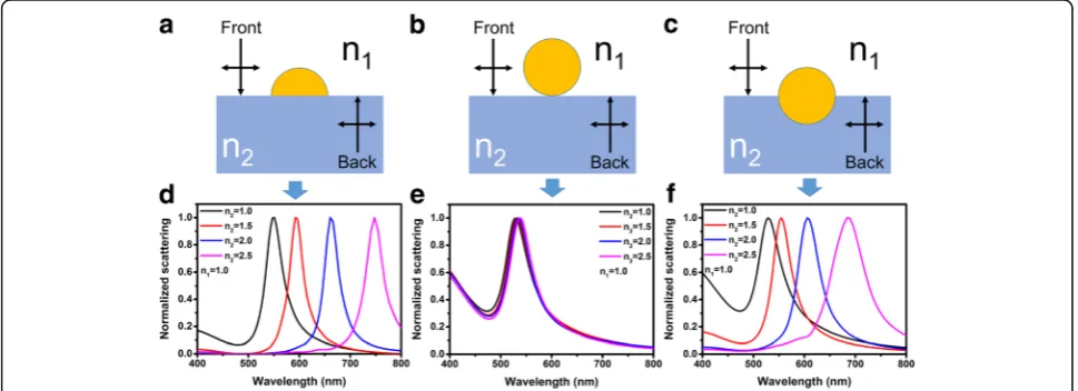
Figure 1a–c shows the schematic illustrations of the structures for FDTD simulations. The structure shown in Fig. 1arepresents the semispherical Au NPs on a di-electric substrate, which is named as structure A. The
structures shown in Fig. 1b represent the spherical Au NPs on a dielectric substrate which is named as structure B. For comparison, the structure C shown in Fig.1c, which have a higher symmetry, is used for simu-lations as well. For simulation, diameters of the Au NPs for all structures are set as 60 nm. The refractive indices of the mediums above the substrates are set asn1= 1 in most cases. The refractive indices of the substrates vary from n2= 1 to n2= 2.5. Figure 1d–f shows the normal-ized scattering spectra of structures A to C, respectively. It is clearly to see that for structure A and C, the scatter-ing peaks redshift with the increasscatter-ing of the refractive indices of the substrates dramatically. However, for structure B, the increase of the refractive indices of the substrates has a negligible effect on the scattering peaks.
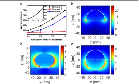
Figure2a shows the wavelength of the LSP scattering maxima vs. the refractive indices of the substrates ex-tracted from Fig. 1. From Fig. 2a, the first information we can obtain is that when the refractive indices of sub-strates increase, the scattering peak wavelengths increase faster than the linearly assumption. This can be approxi-mately explained by the Mie theory. From Mie theory, under the Quasi-Static Approximation, the scattering cross section of a metal NP surrounded by an isotropic and non-absorbing medium with dielectric constant εm can be expressed as:
CS¼
8π 3 k
4
a6 εεþ−εm
2εm
2 ð1Þ
wherekis the wave vector of the propagating wave,ais the radius of a spherical metal NP, andε represents the dielectric constant of the metal. Insert in the Fig. 2a
shows the relationship between the scattering peak wavelengths and the refractive indices of the medium surrounding the metal NP calculated using Eq. (1). One
[image:2.595.56.541.528.704.2]can clearly see the super-linear relationship between the scattering peak wavelengths and the refractive indices which is quite similar to the simulated results. Thus we can use the effective refractive index theory for further discussions. From the effective refractive index theory, if the scattering peak wavelengths of Au NP are sur-rounded by an infinite dielectric medium with refractive indexneffequal to that of the Au NP for different
struc-tures,neffcan be regarded as the effective refractive
indi-ces of the corresponding structures. Table 1 shows the
neffobtained using this method. Using a linear fitting equation [36]:
neff ¼μn1þð1−μÞn2; ð2Þ
where μcan be regarded as the weighting coefficient to
estimate the influence of substrate refractive index to the LSP coupling wavelength. The influence of the me-diums above and below the interface can be estimated. Using the parameters shown in Table 1, the weighting coefficientsμ of structure A to C are 0.38 ± 0.02, 0.93 ± 0.01, and 0.25 ± 0.05, respectively. These results indicate that for structure B, the scattering peak wavelength is al-most dependent on the refractive index of the medium above the interface only. For structure C, the refractive index of the substrate plays an important role to the scattering peak wavelength. However, for structure A, the scattering peak wavelength is affected by the refract-ive index of the mediums above and below the interface both.
[image:3.595.58.539.87.376.2]These phenomena can be explained by the electric field distributions analysis. Figure 2b–d shows the elec-tric field amplitude distributions of structure A to C withn2= 1.5 at the corresponding scattering peak wave-lengths respectively. Electric field concentrated mostly near the interface, both the medium above the interface and the medium below the interface affect the resonance wavelengths of the LSPs for structure A to C, respect-ively. These results confirm that the electric field distri-bution is in good agreement with the calculated weighting coefficients because the influence of the Fig. 2aScattering peak wavelengths of different structures with varying substrate refractive indices. The insert shows the relationship between the LSP coupling wavelength and refractive index of surrounding medium based on Mie theory.b–dPolarization electric field distributions of structure A to C withn2= 1.5 at the corresponding LSP coupling wavelength respectively
Table 1nefffor different structures and with varying substrate
refractive indices
Structure n2 1.00 1.50 2.00 2.50
neff
Structure A 1.00 1.30 1.63 1.96
Structure B 1.00 1.03 1.08 1.12
[image:3.595.58.290.661.731.2]surrounding medium to the scattering peak wavelength can be attributed to the polarization of the dielectric medium caused by the localized electric field.
From Eq. (2), we obtain whenn2is fixed andn1is tun-able, the changing rate, i.e., the slope of the neff, is the weighting coefficients μ. Thus we can use the results above to optimize the LSP-based chemical sensor if the substrate is unavoidable. LSP-based chemical sensor is to detect the refractive index changing of surrounding environment through the LSP resonance peak wave-length shift Δλ [37]. The sensitivity of the sensors is strongly related to two parameters, including the shift parameterS=d(Δλ)/d(Δn) and the figure of meritFOM =S/FWHM, where Δn represents the change of refract-ive index and FWHM is the full wave at half maximum of initial state [37, 38]. Most of previous studies on LSP-based sensors focus on the material, size, and the shape of the NPs [39–41]. However, very few reports
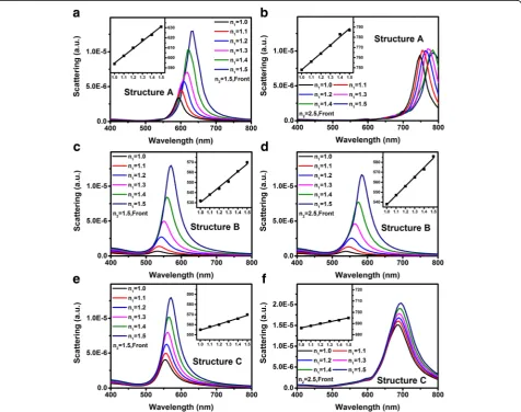
discussed the influence of substrate and their interac-tions with the metal NPs. Figure 3 shows the scattering spectra of structure A to C whenn1is linearly increased from 1.0 to 1.5 and n2 is fixed as 1.5 or 2.5. Inserts shown in all figures represent the scattering peak wave-lengths vs. n1. Figure 3a–f shows that the S parameter for structure A and B is higher than that of structure C. Table2lists the calculated parameters ofS,FWHM, and FOM from Fig.3. For n2= 1.5, the S and FOM parame-ters for structures A and B is much better than that of structure C. However, for n2= 2.5, although the S pa-rameters for structures A and B is higher than that when n2= 1.5, the FOMdeteriorates because of the increasing ofFWHM.
The discussion above is all about the LSP coupling wave-length. While, the LSP coupling strength is another valu-able parameter for many LSP-based devices such as LEDs, photodetectors, solar cells, and emerging techniques such
[image:4.595.61.538.317.693.2]as SERS, TERS, and chemical sensors. Our previous investi-gation indicated that for structure A, the coupling strength between light and LSPs will be influenced by the incident direction of light. This can be attributed to the different local driving electric field intensities when light is normally incident from the air and the substrate [26]. The ratio of the extinction peak intensities when light is incident from the substrate (denoted as back incidence) and the air (de-noted as front incidence)CB/CFis equal to n2/n1. Figure4 shows the FDTD-simulated scattering spectra when light is incident from different directions, associated with the scat-tering spectra of Au NPs surrounded by the corresponding effective refractive indices. Figure4a–c,d–frepresents the scattering spectra of structures A and C respectively. The refractive indices of the substraten2are 1.5, 2.0, and 2.5 for Fig. 4a, d, b, e, c, f, respectively. n1is fixed as 1.0 for all spectra. Similar to the extinction spectra, the scattering peak intensities when light is incident from back and front CSB/CSFis equal ton2/n1for structure A and C both.
When we take the scattering spectra of Au NPs sur-rounded by the corresponding effective refractive indices into account, there are difference between the scattering peak intensities of structure A and C. Figure5a,bshows the ratios of CSF/CSeff and CSB/CSeff vs. the refractive
indices of substrates of structure A and C respectively, whereCSeffis the scattering peak intensities of which the Au NPs are surrounded by infinite dielectric mediums with effective refractive indices (Fig. 4). For all sub-strates, the ratios CSF/CSeff and CSB/CSeff of structure A are smaller than those of structure C. This can also be explained by the difference between the local driving electric field of structure A and C.
Based on the modified Fresnel equations [26, 42], the intensity of the local driving electric field when light is incident from the front and back sides can be written as 2n1Ei/(n1+n2+A) and 2n2Ei/(n1+n2+A), where Ei is the electric field intensity of the incident wave, andA=
−i(ω/c)ρα can be regarded as an additional parameter arising from the LSPs, which is proportional to the po-larizabilityαof the Au NPs and is a positive real number at the LSP resonance frequency. Thus the CSB/CSF is equal ton2/n1which is shown in Fig. 4 as well. On the other hand, the local driving electric field intensity when the Au NPs surrounded by the corresponding effective refractive index is equal toEi. Thus the value ofA par-ameter can be obtained using the equation:
2n1
n1þn2þA¼
CSF
CSeff;
and 2n2
n1þn2þA¼
CSB
CSeff: ð
3Þ
[image:5.595.57.291.111.207.2]The calculated Aparameters are listed near the corre-sponding point in Fig.5a,b. One can see that the value of Ais very close but not exactly the same for different light incident directions. This is attributed to the slightly difference between CSB/CSF and n2/n1as well as the ac-curacy of the simulation software. For the same struc-ture with different substrate refractive indices, the A value increases with the increasing of the substrate re-fractive indices, which can be attributed to the increased
Table 2Scattering peak wavelengths, performance parameters SandFOMof structure A to C calculated from Fig.3
Model n2 S(nm/RIU) FWHM(nm) FOM(RIU−1)
Structure A 1.5 74 46 1.61
2.5 78 56 1.36
Structure B 1.5 76 44 1.73
2.5 96 64 1.50
Structure C 1.5 30 52 0.54
2.5 18 74 0.24
[image:5.595.58.539.517.696.2]polarizability of the Au NPs with the increasing of the LSP resonance wavelength [43–45]. One the other hand, one should be aware that the Avalue of structure A is much bigger than that of structure C for different struc-tures with the same substrate refractive indices. It means that the polarizability of the Au NPs for structure A is much bigger than that of structure C, which can be proven by Fig. 2b, d. It is interesting that although the polarizability of the Au NPs of structure A is bigger than that of structure C, the scattering peak intensities of structure A is smaller than that of structure C (Fig. 4). This can be attributed to the higher absorption of struc-ture A. Figure5c,dshows the scattering and absorption spectra of structure A and C respectively, the refractive index of the substrate is 2.0 for both structures and light is incident from back side. One can see that the absorp-tion of structure A is much higher than that of structure C. Thus for structure A, most of the energy that excite the LSPs is consumed via absorption and does not scattered.
However, for structure B, the ratio CSB/CSF does not equal ton2/n1. Figure6a–cpresents the scattering spec-tra of structure B with different subsspec-trate refractive indi-ces of 1.5, 2.0, and 2.5 respectively. CSB/CSFof structure B is smaller thann2/n1for all substrate refractive indices. As schematically illustrated in Fig.6d, when light is inci-dent from front side, the local driving electric field can be written as the superposition of Ei and ErF, where ErF
is the electric field intensity of the reflected wave. The local driving electric field intensity when light is incident from the front side can be written as EdF ¼EiþErF ¼ ½ 1þn1−n2
n1þn2 cosð
4πPa
λLSPÞEi, wherePis a coefficient that relate
to the average distance of the oscillating electrons and an additional light path when light is propagating through the Au NPs, and theλLSPis the resonance wave-length of the LSPs. Considering that the local driving electric field intensity when light is incident from the back side can be written as EdB=EtB= 2n2Ei/(n1+n2), the ratio of the local driving electric field intensities when light is incident from back and front sides can be written as:
EdB
EdF ¼
2n2
n1þn2
ð Þ þðn1−n2Þcos 4ð πPa=λLSPÞ ð4Þ
Table 3 listed the CSB/CSF of structure B obtained by the scattering spectra and the EdB/EdF calculated using Eq. (4) with different P coefficients. One can see that when the Pcoefficient equals to 1.5, EdB/EdF is in good accord with the ratios ofCSB/CSFfor all substrates. The reason whyPequals to 1.5 is still unclear.
[image:6.595.57.539.88.347.2]One can see that for Au NPs with difference sizes, when the P coefficient is equal to 1.5, the ratios of CSB/CSF and EdB/EdF agree with each other quite well whenever the NPs are oblate elliptical or prolate elliptical. Table5 shows that thePcoefficient of the Ag NPs with different sizes equals to 1.5 as well. Thus thePcoefficient is rela-tively universal, indicating there should be an internal mechanism for the P coefficient and worth further in-depth investigation.
The discussions above are based on single NP. How-ever, in the practice, array structures of nanoparticles are usually achieved for investigation. Thus NP dimers should be employed for discussion because the near field properties of the periodic NP structures will be affected by boundary condition issues in FDTD simulations. The geometric structure parameters of the NPs used for the dimer simulation are similar to that for the single NP discussed above, and a 2 nm gap is set between these two NPs. The simulated results (not shown here) dem-onstrated that when the polarization direction of
normally incident light is perpendicular to the NP dimer, all properties is the same to that as shown for single NP. Thus all near field properties discussed below are based on an incident light of which the polarization direction is parallel to the NP dimer.
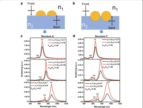
[image:7.595.58.539.87.346.2]Figure7a,bshows the schematic illustrations of semi-spherical Au dimers on a dielectric substrate (structure A′) and spherical Au dimers half-buried into the sub-strate (structure C′) respectively. Figure 7c,dshows the scattering spectra of the dimers with different substrate refractive indices and light incident directions. One can see that for structure A′and C′, both the first-order and the second-order scattering peaks are observed in all spectra. Particularly, for structure C′, the third-order peaks can be observed when the refractive indices of the substrate is equal to 2 and 2.5. One can also see that all Fig. 6a–cScattering spectra for varyingn2= 1.5, 2.0, and 2.5 of structure B respectively. Black and red lines represent the front and back incident cases respectively.dSchematic diagram of local driving electric field of structure B for different incident directions
Table 3SimulatedCSB/CSFand calculatedEdB/EdFusing Eq. (4)
of structure B with differentPcoefficients
n2 Peak
wavelengths (nm)
CSB/
CSF
EdB/EdF
P= 1.0 P= 1.5 P= 2.0
1.5 532 1.33 1.41 1.33 1.24
2.0 535 1.59 1.79 1.59 1.41
[image:7.595.305.538.620.731.2]2.5 538 1.79 2.12 1.81 1.54
Table 4SimulatedCSB/CSFand calculatedEdB/EdFusing Eq. (4)
whenPequals 1.5 of different sizes, shapes of Au NPs whenn2
fixed as 1.5
Model Axial length (nm) CSB/
CSF
EdB/EdF (P= 1.5)
x y z
Au oblate ellipsoid
80 80 60 1.32 1.34
75 75 50 1.36 1.38
60 60 40 1.42 1.42
Au prolate ellipsoid
40 40 60 1.33 1.33
33.4 33.4 50 1.38 1.37
[image:7.595.56.292.658.732.2]scattering peaks redshift greatly with the increase of the substrate refractive indices. This can be explained by the electric field amplitude distributions at the correspond-ing wavelengths of the first-order peak for structure A′ and C′as shown in Fig.8a, b, respectively, the refractive indices of the substrate is 1.5. Similar to that as shown in Fig. 2, the electric field concentrated mostly near the
interface. Thus when light is incident from different di-rections, an equal of CSB/CSF to n2/n1 can be expected and as demonstrated in Fig. 7c, d. On the other hand, comparing with the scattering spectra as shown in Fig. 4, the scattering peak intensities of the dimer are much higher than that of the single NP. This is attributed to the great electric field enhancement by the hot spots at the nano gaps [33].
[image:8.595.57.291.121.229.2]However, as shown in Fig.9, for spherical Au dimers lo-cated on a dielectric substrate (structure B′), the influence by the refractive index of the substrate is slightly stronger than that for structure B. The first-order peak redshifts from 580 to 614 nm when the refractive index of the sub-strate is increased from 1.5 to 2.5, of which is larger than that for single NP (from 532 to 538 nm). This may be at-tributed to the electric field amplitude distributions at the corresponding peak wavelength of the first-order peak for structure B′(Fig.9d, the refractive index of the substrate is 1.5). The electric field intensity in the substrate is stronger than that shown in Fig.2c. As well, as shown in Fig.9, the
Table 5SimulatedCSB/CSFand calculatedEdB/EdFusing Eq. (4)
whenPequals 1.5 of different sizes and material of spherical NPs whenn2fixed as 1.5
Model Axial length (nm) CSB/
CSF
EdB/EdF (P= 1.5)
x y z
Au sphere 60 60 60 1.33 1.33
50 50 50 1.39 1.37
40 40 40 1.43 1.41
Ag sphere 60 60 60 1.23 1.22
50 50 50 1.30 1.28
40 40 40 1.38 1.35
[image:8.595.58.539.342.703.2]ratio of CSB/CSF for NP dimers of structure B′ does not equal ton2/n1, similar to that for single NP. However, theP parameter is no longer a constant if Eq. (4) is still applied. ThePparameters can be calculated to 1.67, 1.82, and 2.05 when the refractive index of the substrate is 1.5, 2.0, and 2.5, respectively. The difference between the P parameter for structure B and B′needs further investigations.
Conclusions
In summary, the impact of the substrate on the coupling wavelength and strength of LSPs have been studied by FDTD simulation and theoretical analysis. For the struc-tures with hemispherical Au NPs located on substrate and spherical Au NPs half-buried into the substrate, the LSP coupling wavelength varies greatly with the refractive index of the substrate. However, the dependency of the
LSP coupling wavelength onto substrate is marginal for the structure that spherical Au NPs are located on the substrate. The dependency difference has been explained by the polarization field distributions of LSPs for different structures. For the structure of which spherical Au NPs is half-buried into the substrate, the polarization field of LSPs is concentrated in the medium above the substrate. However, the polarization fields penetrate into the sub-strate greatly for the other two structures. In addition, the LSP coupling strengths of these three structures have also been studied by changing the incident direction of light, either normally from air or substrate. Simulated results show that for the structures with hemispherical NPs lo-cated on the substrate and spherical NPs half-buried into the substrate, the ratio of the scattering peak intensities for different light incident directions is equal to the ratio Fig. 8a,bPolarization electric field distributions of structure A′and C′withn2= 1.5 at the corresponding wavelengths of the first order peak respectively
[image:9.595.57.539.87.193.2] [image:9.595.57.540.440.692.2]of the refractive indices of the incidence medium and the exiting medium. However, for the structure of which spherical NPs are located on the substrate, these two ra-tios do not equal to each other. These phenomena have been quantitatively explained by considering the local driving electric field intensities of the LSPs using modified Fresnel equations. The near field property of NP dimers is also calculated. Although multiple order peaks are shown in the scattering spectra, the scattering peak wavelengths redshift greatly for structures with substrate refractive in-dices for hemispherical Au dimers located on substrate and spherical Au dimers half-buried into the substrate. The ratio of the scattering peak intensities for different light incident directions is equal to the ratio of the refract-ive indices of the incidence medium and the exiting medium as well. However, for Au dimers located on the substrate, the influence induced by the refractive index of the substrates is slightly stronger than that for single spherical Au NP located on the substrate.
Methods
The models of hemi-/spherical metal NP located on sub-strate (denoted as structures A and B) and spherical metal NP half-buried into substrate (denoted as structure C) are created and studied by Lumerical FDTD (version 8.15.736), a commercial finite-difference time-domain solver. The substrate is semi-infinite in thezaxis and infinite in thex/y axis. The size of NP is set as 60 nm in diameter. The re-fractive index parameter of metal, gold, and silver specific-ally are support by CRC [46]. Total-field scattered-field source (TFSF), a special designing light source for studying particle scattering, is adopted in our research. The light normally incident from +zdirection (designed as front in-cident) and−z direction (designed as back incident). Per-fectly matched layers (PMLs) were used to absorb the scattered radiation in all directions (in order to eliminate reflection back to the model). The PML parameters such as Kappa, Sigma, layers, and polynomial order are assumed by 2, 1, 32, and 3 respectively. In addition, FDTD method con-sists in introducing a space and time mesh that must satisfy the stability criterion [47]. In order to converge, the simula-tion time and time steps (dt) are set to 2000 fs and 0.07 fs respectively. The space mesh is set to 0.3 nm in every direc-tion (dx=dy=dz).
Abbreviations
FDTD:Finite-difference time-domain; LSP: Localized surface plasmon; NPs: Nanoparticles; SERS: Surface-enhanced Raman scattering; TERS: Tip-enhanced Raman scattering; TFSF: Total-field scattered-field
Funding
This work was supported by the National Key Research and Development Program (2016YFB0400903), the National Natural Science Foundation of China (U1405253, 61604124 and 61874090), the Natural Science Foundation of Fujian Province (2017J01121), and the fundamental research funds for the central universities (20720160018 and 20720170098).
Authors’Contributions
JWL performed the FDTD simulation and drafted the manuscript. KH, NG, LJ, JZ, PGL, ETY, and JYK took part in the discussion of results. KH and NG participated in the conception of the project, revised the manuscript, and coordinated between all the participants. All authors read and approve the final manuscript.
Competing Interests
The authors declare that they have no competing interests.
Publisher’s Note
Springer Nature remains neutral with regard to jurisdictional claims in published maps and institutional affiliations.
Author details 1
Fujian Provincial Key Laboratory of Semiconductors and Applications, Collaborative Innovation Center for Optoelectronic Semiconductors and Efficient Devices, Department of Physics, Xiamen University, Xiamen 361005, People’s Republic of China.2Department of Electrical and Computer Engineering, Microelectronic Research Center, The University of Texas at Austin, Austin, TX 78758, USA.3Inspection and Quarantine Technology Center, Xiamen Entry-Exit Inspection and Quarantine Bureau of the People’s Republic of China, Xiamen 361026, People’s Republic of China.
Received: 17 April 2018 Accepted: 28 August 2018
References
1. Taguchi A, Saito Y, Watanabe K, Yijian S, Kawata S (2012) Tailoring plasmon resonances in the deep-ultraviolet by size-tunable fabrication of aluminum nanostructures. Appl Phys Lett 101(8):081110
2. Nehl CL, Hafner JH (2008) Shape-dependent plasmon resonances of gold nanoparticles. J Mater Chem 18(21):2415
3. Kelly KL, Coronado E, Zhao LL, Schatz GC (2003) The optical properties of metal nanoparticles: the influence of size, shape, and dielectric environment. J Phys Chem B 107(3):668–677
4. Sekhon JS, Verma SS (2012) Rational selection of nanorod plasmons: material, size, and shape dependence mechanism for optical sensors. Plasmonics 7(3):453–459
5. Hutter E, Fendler JH (2014) Exploitation of localized surface plasmon resonance. Adv Mater 16(19):1685–1706
6. Radhakumary C, Sreenivasan K (2011) Gold nanoparticles generated through
“green route”bind Hg2+ with a concomitant blue shift in plasmon absorption peak. Analyst 136(14):2959–2962
7. Huang K, Gao N, Wang C, Chen X, Li J, Li S et al (2014) Top- and bottom-emission-enhanced electroluminescence of deep-UV light-emitting diodes induced by localised surface plasmons. Sci Rep 4:4380
8. Sung J-H, Yang JS, Kim B-S, Choi C-H, Lee M-W, Lee S-G et al (2010) Enhancement of electroluminescence in GaN-based light-emitting diodes by metallic nanoparticles. Appl Phys Lett 96(26):261105
9. Pellegrini G, Mattei G, Mazzoldi P (2009) Light extraction with dielectric Nanoantenna arrays. ACS Nano 3(9):2715–2721
10. Liu Y, Zhang X, Su J, Li H, Zhang Q, Gao Y (2014) Ag nanoparticles@ZnO nanowire composite arrays: an absorption enhanced UV photodetector. Opt Express 22(24):30148–30155
11. Butun S, Cinel NA, Ozbay E (2012) LSPR enhanced MSM UV photodetectors. Nanotechnology 23(44):444010
12. Qiao L, Wang D, Zuo L, Ye Y, Qian J, Chen H et al (2011) Localized surface plasmon resonance enhanced organic solar cell with gold nanospheres. Appl Energy 88(3):848–852
13. Hägglund C, Zäch M, Petersson G, Kasemo B (2008) Electromagnetic coupling of light into a silicon solar cell by nanodisk plasmons. Appl Phys Lett 92(5):053110
14. Kalachyova Y, Mares D, Jerabek V, Ulbrich P, Lapcak L, Svorcik V et al (2017) Ultrasensitive and reproducible SERS platform of coupled Ag grating with multibranched Au nanoparticles. Phys Chem Chem Phys 19:14761–14769 15. Kalachyova Y, Mares D, Jerabek V, Zaruba K, Ulbrich P, Lapcak L et al (2016)
The effect of silver grating and nanoparticles grafting for LSP-SPP coupling and SERS response intensification. J Phys Chem C 120:10569–10577 16. Zhou Y, Li XH, Ren XG, Yang LB, Liu JH et al (2014) Designing and
grating coupling system for highly intensified surface-enhanced Raman spectroscopy. Analyst 139:4799–4805
17. Liu Y, Xu SP, Li HB, Jian XG, Xu WQ et al (2011) Localized and propagating surface plasmon co-enhanced Raman spectroscopy based on evanescent field excitation. Chem Commun 47:3784–3786
18. Wallace GQ, Pashaee F, Hou R, Tabatabei M, Lagugne-Labarthet F (2014) Plasmonic nanostructures for enhanced Raman spectroscopy: SERS and TERS of thiolated monolayers. In: Andrews DL, Nunzi JM, Ostendorf A (eds) Nanophotonics V. Proceedings of SPIE. 9126. Spie-Int Soc Optical Engineering, Bellingham
19. Schultz ZD, Marr JM, Wang H (2014) Tip enhanced Raman scattering: plasmonic enhancements for nanoscale chemical analysis. Nanophotonics 3(1–2):91–104
20. Barbillon G, Bijeon JL, Plain J, de la Chapelle ML, Adam PM, Royer P (2007) Electron beam lithography designed chemical nanosensors based on localized surface plasmon resonance. Surf Sci 601(21):5057–5061 21. Saha K, Agasti SS, Kim C, Li XN, Rotello VM (2012) Gold nanoparticles in
chemical and biological sensing. Chem Rev 112(5):2739–2779 22. Malinsky DM, Kelly KL, Schatz GC, Van Duyne RP (2001) Nanosphere
lithography: effect of substrate on the localized surface plasmon resonance spectrum of silver nanoparticles. J Phys Chem B 105:2343–2350
23. Ringe E, McMahon JM, Sohn K, Cobley C, Xia YN, Huang JX et al (2010) Unraveling the effects of size, composition, and substrate on the localized surface plasmon resonance frequencies of gold and silver nanocubes: a systematic single-particle approach. J Phys Chem C 114:12511–12516 24. McMahon JM, Wang Y, Sherry LJ, et al (2009) Correlating the structure,
optical spectra, and electrodynamics of single silver nanocubes. J Phys Chem C 114:12511-12516
25. Zhang SP, Bao K, Halas NJ, Xu HX, Nordlander P (2011) Substrate-induced fano resonances of a plasmonic nanocube: a route to increased-sensitivity localized surface plasmonresonance sensors revealed. Nano Lett 11:1657–1663
26. Huang K, Pan W, Zhu JF, Li JC, Gao N, Liu C et al (2015) Asymmetric light reflectance from metal nanoparticle arrays on dielectric surfaces. Sci Rep 5:18331
27. Tan BJY, Sow CH, Koh TS, Chin KC, Wee ATS, Ong CK (2005) Fabrication of size-tunable gold nanoparticles array with nanosphere lithography, reactive ion etching, and thermal annealing. J Phys Chem B 109(22):11100–11109 28. Aslan K, Leonenko Z, Lakowicz JR, Geddes CD (2005) Annealed silver-island
films for applications in metal-enhanced fluorescence: interpretation in terms of radiating plasmons. J Fluoresc 15(5):643–654
29. Ko SH, Park I, Pan H, Grigoropoulos CP, Pisano AP, Luscombe CK et al (2007) Direct nanoimprinting of metal nanoparticles for nanoscale electronics fabrication. Nano Lett 7(7):1869–1877
30. Jana NR, Gearheart L, Murphy CJ (2001) Wet chemical synthesis of high aspect ratio cylindrical gold nanorods. J Phys Chem B 105(19):4065–4067 31. Sau TK, Rogach AL (2010) Nonspherical noble metal nanoparticles:
colloid-chemical synthesis and morphology control. Adv Mater 22(16):1781–1804 32. Yang Z, Chen S, Fang P, Ren B, Girault HH, Tian Z (2013) LSPR properties of
metal nanoparticles adsorbed at a liquid–liquid interface. Phys Chem Chem Phys 15(15):5374
33. Wu DJ, Cheng Y, Liu XJ (2009)“Hot spots”induced near-field enhancements in Au nanoshell and Au nanoshell dimer. Appl Phys B Lasers Opt 97:497–503 34. Shen Z, Su L et al (2016) Plasmonic trapping and tuning of a gold
nanoparticle dimer. Opt Express 24(5):4801–4811
35. Lecarme O, Tatiana PR, Berton K, Berthier J, Peyrade D et al (2011) Plasmonic coupling in nondipolar gold colloidal dimers. Appl Phys Lett 98:083122 36. Novo C, Funston AM, Pastoriza-Santos I, Liz-Marzan LM, Mulvaney P (2008)
Influence of the medium refractive index on the optical properties of single gold triangular prisms on a substrate. J Phys Chem C 112(1):3–7
37. Mayer KM, Hafner JH (2011) Localized surface plasmon resonance sensors. Chem Rev 111(6):3828–3857
38. Sherry LJ, Chang SH, Schatz GC, Van Duyne RP, Wiley BJ, Xia YN (2005) Localized surface plasmon resonance spectroscopy of single silver nanocubes. Nano Lett 5(10):2034–2038
39. Haes AJ, Haynes CL, McFarland AD, Schatz GC, Van Duyne RP, Zou S (2011) Plasmonic materials for surface-enhanced sensing and spectroscopy. MRS Bull 30(05):368–375
40. Chen HJ, Kou XS, Yang Z, Ni WH, Wang JF (2008) Shape- and size-dependent refractive index sensitivity of gold nanoparticles. Langmuir 24(10):5233–5237
41. Lee KS, El-Sayed MA (2006) Gold and silver nanoparticles in sensing and imaging: sensitivity of plasmon response to size, shape, and metal composition. J Phys Chem B 110(39):19220–19225
42. Bedeaux D, Vlieger J (2001) Optical properties of surfaces. Imperial Collage Press, London
43. Liaw JW, Lo WJ, Kuo MK (2014) Wavelength-dependent longitudinal polarizability of gold nanorod on optical torques. Opt Express 22(9):10858–10867
44. Auguie B, Barnes WL (2008) Collective resonances in gold nanoparticle arrays. Phys Rev Lett 101(14):143902
45. Maier SA (2007) Plasmonics: fundamentals and applications. Springer, New York
46. Weast RC et al (1981) Handbook of chemistry and physics, 61st edn. CRC, Boca Raton