ISSN (e): 2250-3021, ISSN (p): 2278-8719
Vol. 08, Issue 6 (June. 2018), ||V (VII) || PP 16-22
Performance analysis of CdTe solar cell using different
n-type Layers
1
Anjali Thakur ,
2Rajesh Mehra ,
3Neha Thakur
1,2,3
(Electronics & Communication Engineering Department, National Institute of Technical Teachers Training & Research
Chandigarh, UT, India) Corresponding Author: Anjali Thakur
Abstract:
Cadmium Telluride (CdTe) is the main contender for the advancement of more affordable, monetarily suitable photovoltaic (PV) devices among thin-film solar cells. CdTe is the first Photovoltaic technology at a low cost. It has a band gap of 1.45 eV and has high optical absorption coefficient and chemical stability. Because of these properties CdTe is the most appropriate material for design of solar cells. This paper deals with structure parameters of the CdTe solar cell affirmed by basic theories, trials,reports and experiments. The impact of composition on the short circuit current, fill factor, open circuit voltage and the conversion efficiency are talked about in this paper. The simulated devices are analyzed and compared using CdS, CdZnS and ZnO: Al. The designed and simulated model use different n-type layers and results were analyzed. The structure using CdZnS provides 3.34% better efficiency than using CdS. The structure using CdS provides 1.48% better efficiency than using ZnO: Al as n-type layer.--- --- Date of Submission: 10-06-2018 Date of acceptance: 29-06-2018 --- ---
I.
INTRODUCTION
Solar cell is a device that converts light energy into electricity. Solar Cells are grouped together into larger units called modules and into solar panels. Solar Cell is created by two different layers of semiconductor i.e. p-type and n-type such that they sandwiched together to create a junction. When sunlight falls on depletion region, it makes holes to enter in p-type region and electrons in n-type region., thus generating a higher flow of electricity. When light falls on depletion region, then it destroys the neutral atoms, it makes electrons excites to the conduction band from valence band [1]. In solar cell, the n type semiconductor is thick so that light falls on the depletion layer with high intensity. Solar cells are classified into three generations. The first generation uses materials polysilicon and monocrystalline silicon. Silicon solar cells has low cost so they used in most of the applications and they also have easy to fabricate. But the drawback with silicon material is that they have low absorption coefficient of the photons whose wavelength are nearer to the bandgap as silicon is indirect bandgap material.
SUNLIGHT
Metal Contact
n-type
p-type
Metal Contact
Fig.1 Solar Cell Structure
quantum productivity thermodynamic proficiency, quantum effectiveness fill factor and VOC proportion. Reflectance losses is a bit of quantum productivity under "outer quantum proficiency". Recombination misfortunes make up another segment of quantum proficiency, VOC ratio, and fill factor. Fill factor consists Resistive losses factor, and quantum efficiency. The ratio of the maximum obtainable power to the product of the open circuit voltage and short circuit current is known as fillfactor [3].
The solar cells are used in different areas such as Sunlight based Thermal Electric Power Plants: Solar warm vitality includes outfitting solar based power for functional applications from solar based warming to electrical power age. Sun powered warm authorities, for example, sun oriented heated water boards, are regularly used to produce sun powered high temp water for local and light mechanical applications. This vitality framework is likewise utilized as a part of engineering and building configuration to control warming and ventilation in both dynamic sun based and inactive sun-oriented outlines. Photovoltaics: Photovoltaic or PV innovation utilizes sun-oriented cells or sun powered photovoltaic clusters to change over vitality from the sun into power. Sun oriented cells deliver coordinate current power from the sun's beams, which can be utilized to control hardware or to energize batteries. Numerous pocket number crunchers join a solitary solar cell, however for bigger applications, cells are by and large gathered together to shape PV modules that are thus masterminded in solar oriented exhibits. Solar cell clusters can be utilized to control circling satellites and other rocket, and in remote territories as an onset of energy for roadside crisis phones, remote detecting, and cathodic assurance of pipelines [4].
II.
CDTE SOLAR CELL
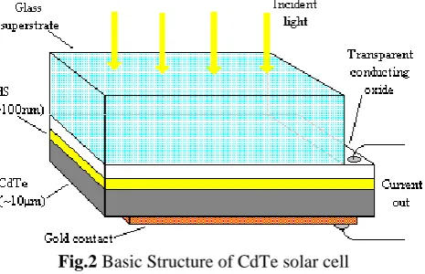
Use of Cadmium telluride has some advantages over silicon. It is thin as compared to the silicon. Additionally, CdTe requires less vitality to change over light into power than silicon. Cadmium Telluride (CdTe) is the principal Photovolatic innovation with ease and has a band hole of ~1.45 eV.It has high absorption coefficient and chemical stability. Due to these properties, CdTe is the most efficient material for design of solar cells. Because of direct bandgap semiconductor, the ingestion of light is simple and it enhances the efficiency. CdTe-based photovoltaic cells is seen as a thin-film as they are microns thick, or about a tenth the estimation of a human hair. CdTe has a direct band gap with high absorption coefficient of 5 × 1015cm[5]. N-type CdS as transparent window is one of the best choice for CdTe heterojunction structures. They are fabricated in a superstrate configuration. Between the CdTe and CdS layer, there is lattice mismatch of 10% but has angood electrical behavior that leads to a high fill factor [6]. CdS/CdTe thin-film solar cells has currently several challenges:The electron hole pair recombination at the CdTe/CdS interface leads to shorter minority carrier .The transparency of transparent conductive oxide (TCO)and CdS window layers is not sufficient [7].Straightforward Conducting Oxide (TCO) layers, for instance, SnO2 or Cd2SnO4 are direct to unmistakable
light and exceedingly conductive to transport current capably. Center layers, for instance, CdS help in both the advancement and electrical properties between the TCO and CdTe. The CdTe film acts as the basic photo conversion layer. The basic structure of CdTe solar cell consists two n-type and p-type layers. Metal is determined to the back to shape electrical contacts. In progress, each one of these layers are saved money on moving toward glass and arranged into complete sun-based sheets in just two or three hours.
Fig.2 Basic Structure of CdTe solar cell
many several hurdles for making CdS/CdTe thin-film solar cells, as there are lattice mismatch problems and many more but has an excellent electrical behavior, leading to a high fill factor makes it effective [8].
III.
DESIGN PARAMETER AND SIMULATION
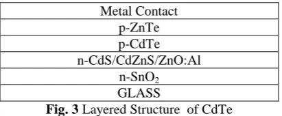
This paper structures of CdTe solar cell comprises n-type CdS, CdZnS and ZnO: Al were analyzed and their results were compared. SnO2 is used as TCO layer as it is being direct to unmistakable light and
exceedingly conductive to transport current capably [9]. CdTe is used as absorber layer as its bandgap is 1.45eV. ZnTe is used as buffer layer. ZnTe has bandgap of 2.26 eV, it results to increase the open circuit voltage. It eliminates the effect of backsurface recombination velocity. The structure of CdTe solar-cell consists two n and p type layers. In this paper, the CdS layer is replaced by CdZnS and ZnO: Al layers and result of those structures were compared with the CdS/CdTe structure.
Metal Contact p-ZnTe p-CdTe n-CdS/CdZnS/ZnO:Al n-SnO2 GLASS
Fig. 3 Layered Structure of CdTe
Fig3 shows the layers of CdTe solar cell. CdTePhotovoltaic cell has the smallest carbon footprint and shortest energy retribution time of all solar technologies. CdTe has bandgap of 1.5 eV at 300K [10]. The thickness of the layers is determined to increase the efficiency of the solar cell. ZnTe is used as buffer layer to reduce the effect of back surface recombination velocity. The band gap of CdS is 2.42 eV, the band gap of CdZnS is 2.48 eV [11] and the band gap of ZnO: Alis 3.3 eV [12]. It consists n-type CdS/CdZnS/ZnO: Al and p-type CdTe to form the junction.
Table no 1 Material Parameters
Parameter CdTe
[10] CdS [12] CdZnS [10] ZnO:Al [12]
Thickness(𝞵m) 4 0.07 0.05 0.01
Bandgap(eV) 1.5 2.42 2.48 3.30
Dielectric Constant 9.4 10 9.3 9
Electron affinity(eV) 4.28 4.5 4.46 4.35
Electron mobility(cm2/Vs) 320 350 100 100
Hole mobility(cm2/Vs) 40 50 40 25
NC (cm-3) 8x10¹⁷ 1.8x10¹⁹ 2.1x10¹⁸ 2.2x10¹⁸
NV (cm-3) 1.8x10¹⁹ 2.4x10¹⁸ 1.7x10¹⁹ 1.8x10¹⁹
n,p(cm-3) 2x10¹⁴ 1x10¹⁷ 1x10¹⁵ 1x10¹⁸
Table 1 shows the material parameters that are used in simulation of structures.Bandgap (Eg) ,Dielectric constant, electron affinity(𝟀) ,Electron mobility ,Hole mobility ,Conduction Band effective density of states (Nc),Valence Band effective density of states (Nv), shallow uniform donor /acceptor density ND (n,p) of the materials /layers used in structures.The thickness of layers were taken in 𝞵m . the width of CdTe is 4 𝞵m ,ZnTe is 0.2 𝞵m, SnO2 is 2 𝞵m in all structures.The width of n-type layers that are varied is taken to be 0.1 𝞵m.
IV.
RESULTS AND DISCUSSION
When the solar cell is simulated in SCAPS. The results were analyzed. The band diagram, current voltage graph, carrier density and current density graphs were analyzed. The device is simulated using Glass/SnO2/CdS/CdTe/ ZnTe. Instead of CdS, CdZnS and ZnO: Al were used in other structures. The result of
three structures were analyzed in terms of efficiency, fill factor, open circuit voltage and short circuit current density.
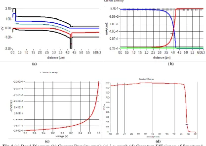
1.Configuration of Glass/SnO2/CdS/CdTe/ZnTe structure
maximum efficiency is obtained at 0. 01𝞵m.The efficiency, increases as the thickness of CdS layer decreases due to shorter transmission path for absorbable photons. Fill Factor increases with the thickness. The absorber thickness is 4𝞵m. Performance analysis of CdS/CdTe solar cell structure is shown in figure 4. Fig (a)shows energy band diagram of CdS/CdTe structure (b) Current Density graph (c) shows the v-i characteristics of solar cell., maximum Isc obtained at 0.01 𝞵m is 28.79 mA/cm2.Figure (d) showing the quantum efficiency curve as a function of wavelength. The quantum efficiency is constant in the region 520 nm to 810 nm and then it decreases and has an onset even up to 900 nm. The defect density is used in structure is 1013 cm-3.
(a) ( b)
(c) (d)
Fig 4 (a) Band Diagram (b) Current Density graph (c) i-v graph (d) Quantum Efficiency of Structure1
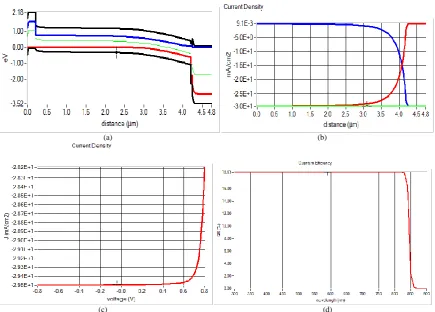
2 Configuration of Glass/SnO2/CdZnS/CdTe/ZnTe structure
(a) (b)
(c) (d)
Fig 5 (a) Band Diagram (b) Current Density graph (c) i-v graph (d) Quantum Efficiency of Structure2
3.Configuration of Glass/SnO2/ZnO: Al/CdTe/ZnTe structure
(a) ( b)
(c) (d)
Fig 6 (a) Band Diagram (b) Current Density graph (c) i-v graph (d) Quantum Efficiency of Structure2
Table no 2: Result Comparison
Voc(volts) Jsc(mA/cm2) FF (%) Eff. (%)
Structure1(CdS) 9.266 27.72 47.39 19.21
Structure2(CdZnS) 9.828 29.49 77.79 22.55
Structure3(ZnO: Al) 8.82 28.85 68.85 17.73
V. CONCLUSION
The characteristics of solar cell with buffer layer ZnTe in CdS/CdTe solar cell were analyzed using same thickness of layers , the output results are Voc is 9.266 volts, Jsc is 27.72mA/cm2 ,the fill factor of solar cell is 47.39%.and the efficiency is 19.21%. CdZnS is used as a n-type layer in another CdTe thin film solar cell structure the output results are Voc is 9.828 volts, Jsc is 29.49mA/cm2.the fill factor of solar cell is 77.79%. The efficiency is 22.55%. ZnO: Al is used as a n-type layer in third structure of CdTe thin film solar. the output results are Voc is 8.82 volts, Jsc is 28.85mA/cm2.the fill factor of solar cell is 68.85%. The efficiency is 17.73%.
REFERENCES
[1]. Naba R. Paudel, Jonathan D. Poplawsky, Karren L. Moore, and Yanfa Yan ,”Current Enhancement of CdTe-Based Solar Cells”, IEEE JOURNAL OF PHOTOVOLTAICS, VOL. 5, NO. 5, SEPTEMBER 2015
[2]. Tao Song, Ana Kanevce, and James R. Sites ,” Design of Epitaxial CdTe Solar Cells on InSb Substrates”, IEEE JOURNAL OF PHOTOVOLTAICS, VOL. 5, NO. 6, NOVEMBER 2015
[3]. Dario Narducci, Peter Bermel, Bruno Lorenzi, Ning Wang, Kazuaki Yazawa. "Hybrid and Fully Thermoelectric Solar Harvesting", Springer Nature, 2018
[4]. Navneet Kaur, Rajesh Mehra, Chandni,” Comparative Study of Solar Cell Devices Using Lead and Tin based Perovskite Material Through Numerical Simulation” International Journal for Scientific Research and Development, Vol5, Issue5,2017
[6]. F. Zhou, X. C. Wang, H. C. Wu and C. Z. Zhao, “Achievements and Challenges of CdS/CdTe Solar Cells,” International Journal of Photo Energy, Vol. 2011, 2011, pp. 1-8.
[7]. M. A. Matin, M. M. Aliyu, A. H. Quadery, and N. Amin, “Prospects of novel front and back contacts for high efficiency cadmium telluride thin film solar cells from numerical analysis,” Solar Energy Materials and Solar Cells, vol. 94, no. 9, pp. 1496–1500, 2010
[8]. Ke Zhu, Ye Yang, Jia Li, Weijie Song. "Physical properties of Al-doped ZnO and Ga-doped ZnO thin films prepared by direct current sputtering at room temperature", Journal of Wuhan University of Technology-Mater. Sci. Ed., 2017
[9]. M. D. S. Hossain, N. Amin, M. A. Matin, M. M. Mannir Aliyu, T. Razykov, and K. Sopian, “A numerical study on the prospects of high efficiency ultra-thin ZnxCd1-xS/CdTe solar cell,” Chalcogenide Letters, vol. 8, no. 4, pp. 263–272, 2011
[10]. Xiaobo Xu, Xiaoyan Wang, Wenping Gu, Si Quan, Zan Zhang, “Study on influences of CdZnS buffer layer on CdTe solar cells”,doi: Superlattices and Microstructures 10.1016/j.spmi.2017.05.033
[11]. Xinmei Liu, YangJiang, Fengming Fu ,Weimin Guo , Wenyi Huang, LijunLi, “Facile synthesis of high-quality ZnS, CdS, CdZnS, and CdZnS/ZnS core/shell quantum dots: characterization and diffusion mechanism”, Materials Science in Semiconductor Processing Volume 16, Issue 6, December 2013, Pages 1723-1729
[12]. Ruksana Safa Sultana, Ali Newaz Bahar, Md. Asaduzzaman, Mohammad Maksudur Rahman Bhuiyan,“Numerical dataset for analyzing the performance of highly efficient ultrathin film CdTe solar cell”,2017, pp 336-340