http://www.sciencepublishinggroup.com/j/se doi: 10.11648/j.se.20180602.11
ISSN: 2376-8029 (Print); ISSN: 2376-8037 (Online)
Modeling and Simulation of DC-DC Boost
Converter-Inverter System with Open-Source Software
Scilab/Xcos
Thandar Aung, Tun Lin Naing
Department of Electrical Power Engineering, Mandalay Technological University, Mandalay, Myanmar
Email address:
To cite this article:
Thandar Aung, Tun Lin Naing. Modeling and Simulation of DC-DC Boost Converter-Inverter System with Open-Source Software Scilab/Xcos. Software Engineering. Vol. 6, No. 2, 2018, pp. 27-36. doi: 10.11648/j.se.20180602.11
Received: June 23, 2018; Accepted: July 5, 2018; Published: July 31, 2018
Abstract:
This paper proposes a mathematical modelling of DC-DC boost converter-inverter system and simulation work is carried out using Scilab/Xcos, which is free and open-source software. In this paper a two-stage DC-AC power conversion system is presented. This system consists of two converters, DC-DC boost converter and single-phase inverter. The boost converter converts input DC low voltage into high DC output voltage. The DC output from boost converter is converted into AC output voltage by an inverter. The mathematical model of a DC-AC boost converter-inverter system is presented with four different modes of operations. By using Kirchhoff’s voltage and current law, the system mathematical model is derived from each operation mode. The mathematical model of the proposed system is represented and state-space matrix is derived. Moreover, the steady-state values of the system are also presented. The transient behaviors of the proposed mathematical model are validated with Xcos simulation results.Keywords:
DC-DC Boost Converter, Free and Open-Source, Mathematical Model, Simulation, Single-Phase Inverter1. Introduction
The growing use of renewable energy sources brings new challenges to the energy conversion technology. One of these challenges is related to the fact that the output voltage of low voltage source (e.g. batteries, solar panels) need to be boosted and must be inverted to AC for practical applications. For many areas away from national grid, main energy source is DC power received from solar. Many industrial and household electrical devices use AC power. In application where the AC power is required, that DC power must be needed to change AC power.
Inverter must be used for changing of DC to AC. Inverter converts DC power to AC output 220V. When DC supply voltage is low, inverter must be connected with transformer to get 220V AC output from inverter. By connecting inverter with transformer produces AC output 220V, there exists transformer losses and costs. The aim to overcome this problem is input side of inverter must be connected with boost converter to boost input DC voltage. Boost converters are nonisolated power converters. They step-up low DC input
voltage into high DC output voltage. The boosted DC output from boost converter is fed into inverter and converts that DC voltage into AC output voltage [1].
modelling of two-stage inverter for battery application is derived and verified with simulation results have been discussed in [8]. Simulation of closed loop controlled DC-DC boost converter with inverter system using MATLAB/Simulink for small scale generation plant application has been discussed in [9].
There are many commercially available modelling and simulation software in the market such as PSim, MATLAB/Simulink, etc. Each software has its own merits. In this paper, Scilab/Xcos is chosen for simulation of the proposed system for the following reasons. It is one of open source software for scientific computation (OSSC) and provides powerful computation for engineering and scientific applications. Similar to MATLAB, it consists of Xcos (Scicos) toolbox which provides block diagram editor for constructing simulation model, dynamic system model and graphical design of a control system. Unlike MATLAB, Scilab is a freely distributed and open source software package and it is free of charge. Scilab 6.0.1 can be downloaded from the link [10].
Block diagram and subsystem of active disturbance rejection control system has been described and simulation on Xcos show good effectiveness of the control system has been expressed in [11]. The difference between two software environments, MATLAB and Scilab are described in [12]. Haofu Liao [13] expressed, Scilab or Xcos used computational function block (flags) to improve the computational efficiency of block. Mathematical model of induction motor is expressed in [14] and simulation is done with step-change in speed and load using Scilab/Xcos.
Modelling of Separately Excited DC Motor drive system using Scilab/Xcos tool and discuss the results in [15]. In the review of the previously mentioned works, simulation of boost converter-inverter system with Scilab/Xcos is not found in literature. In this paper, mathematical model of
DC-DC boost converter-inverter system is represented and simulation work is done by using Scilab/Xcos.
The rests of the paper are structured as follows. In section 2, the mathematical model of the system using switched function is expressed. In section 3, simulation results and discussions are presented. Section 4 is the conclusion of the paper.
2. Mathematical Modeling of DC-DC
Boost Converter-Inverter System
Section II consists of two subsections, mathematical model of the system and switched model of the system including steady-state equations.
2.1. Mathematical Model of the System
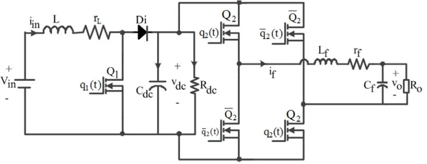
Figure 1 describes the proposed DC-DC boost converter-inverter system. The proposed system combines following three subsections.
(a) Boost Converter, this system consists of inductor (L), inductor parasitic resistance (rL), switching device (Q1),
diode (Di), dc link capacitance (Cdc) and dc link resistance
(Rdc). Where Vin is input voltage, iin is inductor current, q1(t)
is on/off input of Q1 and vdc is dc link voltage. The inductor
stored and released energy when the switch is ON and OFF. The capacitor is used for filtering of ripple in the output voltage [16].
(b) Inverter composes of four switching devices, transistor Q2 and Q2. q2(t) and q t2( )are the ON/OFF control signals of
transistor Q2 and Q2.
(c) LC output filter is connected at the output of inverter. It consists of filter inductor (Lf), filter inductor resistance (rL),
filter capacitance (Cf) and output resistance (Ro). Where if
filter current and output voltage of inverter is isvo.
Figure 1. Proposed DC-DC Boost Converter-Inverter System。
Figure 2. Equivalent Circuit Diagram of DC-DC Boost Converter-Inverter System.
Equivalent circuits of four different modes are represented to derive mathematical models of the system. The differential equations of the proposed system for four different modes are obtained by using Kirchhoff’s voltage and current law.
Mode 1: Q1-OFF and Q2-ON
Figure 3 shows the equivalent circuit when q1=0 and
2 1
q = .
Figure 3. Equivalent Circuit of Mode 1.
The mathematical model of Figure 3 is represented by the following differential equations (1)-(4):
in
in in L dc
di
L V i r v
dt = − − (1)
dc dc
dc in f
dc
dv v
C i i
dt = − −R (2)
f
f dc f f o
di
L v i r v
dt = − − (3)
o o
f f
o
dv v
C i
dt = −R (4)
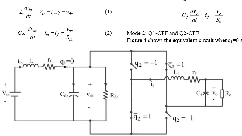
Mode 2: Q1-OFF and Q2-OFF
Figure 4 shows the equivalent circuit whenq1=0 and q2=-1.
The mathematical model of Figure 4 is represented by the following differential equations (5)-(8):
in
in in L dc
di
L V i r v
dt = − − (5)
dc dc
dc in f
dc
dv v
C i i
dt = + −R (6)
f
f dc f f o
di
L v i r v
dt = − − − (7)
o o
f f
o
dv v
C i
dt = −R (8)
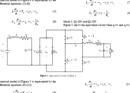
Mode 3: Q1-ON and Q2-ON
Figure 5 shows the equivalent circuit when q1=1 and q2=1.
Figure 5. Equivalent Circuit of Mode 3.
The mathematical model of Figure 5 is represented by the following differential equations (9)-(12):
in
in in L
di
L V i r
dt = − (9)
dc dc
dc f
dc
dv v
C i
dt = − −R (10)
f
f dc f f o
di
L v i r v
dt = − − (11)
o o
f f
o
dv v
C i
dt = −R (12)
Mode 4: Q1-ON and Q2-OFF
Figure 6 shows the equivalent circuit when q1=1 and q2=-1.
Figure 6. Equivalent Circuit of Mode 4.
The mathematical model of Figure 6 is represented by the following differential equations (13)-(16):
in
in in L
di
L V i r
dt = − (13)
dc dc
dc f
dc
dv v
C i
dt = −R (14)
f
f dc f f o
di
L v i r v
dt = − − − (15)
o o
f f
o
dv v
C i
2.2. Switched Function Model of the System
To obtain the dynamic model of the system, equivalent circuit with switches as shown in Figure 2 is considered. Whereas, q1∈{0,1} and q2∈ −{1, 1} are the input switch positions. The switched models of the system can be represented as in (17)-(20):
1
(1 )
in
in in L dc
di
L V i r q v
dt = − − − (17)
1 2
(1 )
dc dc
dc in f
dc
dv v
C q i q i
dt = − − −R (18)
2
f
f dc f f o
di
L q v i r v
dt = − − (19)
o o
f f
o
dv v
C i
dt = −R (20)
In order to obtain the steady-state equation of the system, the average model of the system is used. The switch positions q1 and q2 are replaced by average positions d1 and d2 in
equations (17)-(20). The average switched models of the system are shown in (21)-(24):
1
1
(1 )
in
in in L dc
di
V i r d v
dt L
= − − − (21)
1 2 1 (1 ) dc dc in f dc dc dv v
d i d i
dt C R
= − − −
(22)
2
1
f
dc f f o f
di
d v i r v
dt L
= − − (23)
1 o o f f o dv v i
dt C R
= −
(24)
1 1 ɶ1
d =D +d and d2 =D2+dɶ2, dɶ1<<D1 and dɶ2<< D2 thus
1
ɶ
d and dɶ2 are neglected according to small ripple approximation. d1 and d2 are equal D1 and D2. The system
equilibrium condition can be represented by (25) – (28):
1
1
0 Vin I rin L (1 D V) dc L
= − − − (25)
1 2
1
0 (1 ) in f dc
dc dc
V
D I D I
C R
= − − −
(26)
2
1
0 dc f f o
f
D V I r V
L
= − − (27)
1
0 f o
f o V I C R = −
(28)
In matrix form, equations (25)-(28) can be represented as follow,
1 in
1 2
2
(1 ) 0 0 V
(1 ) 1/ 0 0
0 1 0
0
0 0 1 1/
L in
dc dc
f f
o o
r D I
D R D V
D r I
R V − − − − = − − − (29)
By solving (29), the steady-state matrix is obtained as (30).
2
dc 2 o f
2 2 2
dc 2 o f L dc o dc f dc o 1 dc 1 f dc o 1 dc 1 f
dc o dc f dc o 1 dc 1 f
2
dc 2 o f L dc o dc
(R D + R + r )
((R D + R + r ) r + R R + R r - 2R R D - 2R D r + R R D + R D r ) (R R + R r - R R D - R D r )
((R D + R + r ) r + R R + R
in dc f o I V I V = 2 2
f dc o 1 dc 1 f dc o 1 dc 1 f
dc 2 dc 1 2
2 2 2
dc 2 o f L dc o dc f dc o 1 dc 1 f dc o 1 dc 1 f
dc o 2 dc o 1 2
2
dc 2 o f L dc o
r - 2R R D - 2R D r + R R D + R D r )
(R D - R D D )
((R D + R + r ) r + R R + R r - 2R R D - 2R D r + R R D + R D r ) (R R D - R R D D )
((R D + R + r ) r + R R + R r - 2R R D - 2R D r + R R D + R D r )dc f dc o 1 dc 1 f dc o 12 dc 12f
in V (30)
3. Simulation Results and Discussion
Simulation works and related results are provided in this section.
3.1. Simulation with Scilab/Xcos
Scilab provides a large number of toolboxes for developing and simulation models of several types. The DC-DC boost converter-inverter system (21)-(24) is represented
by using the blocks from Xcos toolbox. Simulation work is important for researchers because it can study dynamic performance of system without any charges. When the system undergoes changes or disturbances, the changes in system dynamic parameters can be easily seen. By doing simulation, it can save time and costs and can easy to study the dynamic changes before practical constructing.
The average duty cycle command of DC-DC boost converter is D1 =0.7. The duty cycle command for reference
is 0.8/1.414. The inverter is intended to generate output voltage of 220 V (rms) and if the power rating is set at 2200
W, the value of load resistance is 22 Ω. The parameters of the system used in simulation are expressed in Table 1.
Table 1. Parameters of the Proposed System.
Parameters Variables Values
Supply voltage Vin 120 [V]
Boost converter frequency f 2000 [Hz]
Inductor L 2 [m H]
Inductor resistance rL 0.2 [Ω]
DC link capacitance Cdc 1.41 [m F]
DC link resistance Rdc 1000 [Ω]
Duty-cycle D1 0.7
D2 (rms) 0.8/ 2
Output filter capacitance Cf 22 [µ F]
Output filter inductance Lf 2 [m H]
Resistance of output filter inductor rf 0.2 [Ω]
Load resistance Ro 22 [Ω]
Output power Po 2200 [W]
Inverter output frequency f 50 [Hz]
Based on (21), the input current block diagram can be created as shown in Figure 7.
Figure 7. Block Diagram of Input Current.
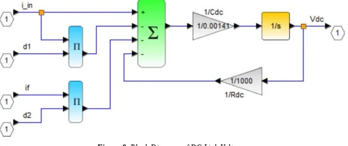
Using (22), the DC-link voltage block diagram can be created as shown in Figure 8.
Figure 8. Block Diagram of DC Link Voltage.
The output filter current block diagram can be created by using (23) as shown in Figure 9.
Based on (24), the inverter output voltage block diagram can be created as shown in Figure 10.
Figure 10. Block Diagram of Output Voltage of Inverter.
By combining the above four block diagrams, the following overall system is obtained. When applying duty cycle commands as inputs and the system is run with Scilab, the output state variables iin, vo, if and vdc are obtained.
Figure 11. Overall System Block Diagram of Boost Converter-Inverter System.
3.2. Discussion on Simulated Results
Table 2 presents the numerical values of the equilibrium points of iin,vdc, ifand vo when the values of DC link resistor Rdc
and output resistor Ro changed at D1=0.7 and D2=0.8/ 2 . The simulation results are shown in Figure 12-14 and discussed the
results.
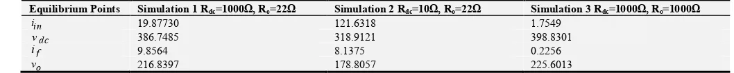
TABLE 2. Simulation Results at the Equilibrium Points.
Equilibrium Points Simulation 1 Rdc=1000Ω, Ro=22Ω Simulation 2 Rdc=10Ω, Ro=22Ω Simulation 3 Rdc=1000Ω, Ro=1000Ω
in
i 19.87730 121.6318 1.7549
dc
v 386.7485 318.9121 398.8301
f
i 9.8564 8.1375 0.2256
o
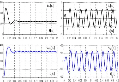
Figure 12. Simulation Results at Rdc=1000Ω and Ro=22Ω.
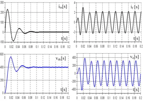
Figure 14. Simulation Results at Rdc=1000Ω and Ro=1000Ω.
The changes in simulation results of iin,vdc,if andvo can
easily be seen in Figure 12-14. Where the value of DC-link resistor decreases, the value of input current dramatically increases with more ripple. The increase in the value of input current damages the devices used in the system. During this condition, the inverter output voltage also decreases. When the value of DC-link resistance is kept constant and load resistance is large nearly opened-circuit, input current value is very small and DC-link voltage changes little. This is due to the existence of DC-link resistor. It protects the sudden increase in DC link voltage when large load resistance changes. The ripple of input current and DC-link voltage are lesser than in simulation-3 as compared with simulation-1. The DC-link voltage fluctuation is more obvious in loaded condition. This is because of power transferred of inverter. The ripple frequency of DC-link voltage fluctuation is twice the output voltage frequency of inverter.
4. Conclusions
In this paper, the configuration of DC-DC boost converter-single phase inverter system has been presented. Mathematical modeling and simulation results of the proposed system have been represented. Simulations of the system have been done by using Scilab/Xcos. The mathematical derivations and analysis have been confirmed with simulation results. As a new user, when using
Scilab/Xcos in faces some unfamiliar problems. But it is free and open source but its computations are reliable solutions. The simulation results are validated with the equilibrium values of table II. As future work, it is intended to control DC-link voltage of DC-DC boost converter-inverter system.
References
[1] R. W. Erickson amd D. Maksimovic, “Fundamental of Power Electronics”, Second Edition.
[2] Victor Hugo Garcia-Rodriguez, Ramon Silva-Ortigoza, Eduardo Hernandez-Marquez, Jose Rafael Garcia-Sanchez, Mario Ponce-Silva and Griselda Saldana-Gonzalez, “A DC Motor Driven by a DC-DC Boost Converter-Inverter: Modeling and Simulation”, 2016 International Conference on Mechatronics and Automotive Engineering (ICMEAE), DOI: 10. 1109/ ICMEAE. 2016. 023.
[3] H. Abdel-Gawad and V. K. Sood, “Small-Signal Analysis of Boost Converter, including Parasitic, operating in CCM”, 2014 6th IEEE Power India International Conference (PIICON), DOI: 10. 1109/POWERI. 2014. 7117622.
[5] Chien-Husan Chang, Chun-A Cheng, Chu-Cheng Chi and Yen-Yu Chen, “Design and Implementation of a Single-Phase Buck-Boost Inverter”, 2017 IEEE 3rd International Future Energy Electronics Conference and ECCE Asia (IFEEC 2017 - ECCE Asia), DOI: 10. 1109/IFEEC. 2017. 7992252. [6] Tiantian Mu, Lei Zhu, Hongfei Wu, Wenying Jiang, “A
Semi-Two-Stage DC-AC Power Conversion System with Improved Efficiency Based on A Dual-input Inverter”, 2016 IEEE Energy Conversion Congress and Exposition (ECCE), DOI: 10. 1109/ ECCE. 2016. 7854773.
[7] C. I. Odeh, “Single Phase DC-AC Boost Converter”, Nigerian Journal of Technology (NIJOTECH), Vol. 33. No. 2, April 2014. pp. 238-244, doi. org: 10. 4314/njt. v33i2. 14.
[8] Yub Hyun, Chang-Soon Lim, Rae-Young Kim, Dong-Seok Hyun, “Averaged Modeling and Control of a Single-Phase Grid-Connected Two-Stage Inverter for Battery Application”, IECON 2013 - 39th Annual Conference of the IEEE Industrial Electronics Society, DOI: 10. 1109/IECON. 2013. 6699184.
[9] Manish Agarwal, Sanjeev Gupta, Sudhir P. Phulambrikar, “Closed Loop DC-DC Boost Converter with Inverter for Small Scale Generation Plant”, International Journal of Engineering Trends and Technology (IJETT) – Volume 15 Number 5 – Sep 2014.
[10] Scilab: Free and Open source Software, http://www.scilab.org/ [11] Lijun Wang, Qing Li, Chaonan Tong, Yixin Yin, Jiangyun Li and Siyang Song, "Active Disturbance Rejection Control
simulation toolbox in open source software Scilab/Xcos," Open-source software for Scientific Computation (OSSC), 2011 IEEE International Workshop, Beijing, China, pp. 71-76, DOI:10. 1109/OSSC. 2011. 6184697.
[12] Zoltan Janik and Katarina Zakova, "Online design of Matlab/Simulink and Scilab/Xcos block schemes," Interactive Collaborative Learning (ICL), 2011 14th International Conference, Slovakia, pp. 241-247, DOI: 10. 1109/ICL. 2011. 6059583.
[13] Haofu Liao, Ping Chen, "Explore a Way of Improving the Computational Efficiency of the Block in SCILAB," Open-source software for Scientific Computation (OSSC), 2011 IEEE International Workshop, Beijing, China, pp. 13-16, DOI:10. 1109/OSC. 2011. 6184686.
[14] Vijay Babu Koreboina and Shankar J Magajikondi, Raju A B, “Scilab/ Xcos Modeling, Simulation and PC Based Implementation of Closed Loop Speed Control of VSI Fed Induction Motor Drive”, 16th National Power Systems Conference, 15th-17thDecember, 2010.
[15] Vinod S. Patil, Sachin Angadi and A. B. Raju, "Four Quadrant Close Loop Speed Control of DC Motor," Circuits, Controls, Communications and Computing (I4C), 2016 International Conference, India, DOI:10. 1109/CIMCA. 2016. 8053305. [16] B. M Hasaneen and Adel A. Elbaset Mohammed, “Design and